EP3853701B1 - Dispositif, son utilisation et système de génération d'un signal périodique sur un capteur superficiel capacitif - Google Patents
Dispositif, son utilisation et système de génération d'un signal périodique sur un capteur superficiel capacitif Download PDFInfo
- Publication number
- EP3853701B1 EP3853701B1 EP19773757.0A EP19773757A EP3853701B1 EP 3853701 B1 EP3853701 B1 EP 3853701B1 EP 19773757 A EP19773757 A EP 19773757A EP 3853701 B1 EP3853701 B1 EP 3853701B1
- Authority
- EP
- European Patent Office
- Prior art keywords
- electrically conductive
- conductive structure
- surface sensor
- periodic signal
- electrode grid
- Prior art date
- Legal status (The legal status is an assumption and is not a legal conclusion. Google has not performed a legal analysis and makes no representation as to the accuracy of the status listed.)
- Active
Links
Images


Classifications
-
- G—PHYSICS
- G06—COMPUTING OR CALCULATING; COUNTING
- G06F—ELECTRIC DIGITAL DATA PROCESSING
- G06F3/00—Input arrangements for transferring data to be processed into a form capable of being handled by the computer; Output arrangements for transferring data from processing unit to output unit, e.g. interface arrangements
- G06F3/01—Input arrangements or combined input and output arrangements for interaction between user and computer
- G06F3/03—Arrangements for converting the position or the displacement of a member into a coded form
- G06F3/041—Digitisers, e.g. for touch screens or touch pads, characterised by the transducing means
- G06F3/0416—Control or interface arrangements specially adapted for digitisers
- G06F3/04166—Details of scanning methods, e.g. sampling time, grouping of sub areas or time sharing with display driving
-
- G—PHYSICS
- G06—COMPUTING OR CALCULATING; COUNTING
- G06F—ELECTRIC DIGITAL DATA PROCESSING
- G06F3/00—Input arrangements for transferring data to be processed into a form capable of being handled by the computer; Output arrangements for transferring data from processing unit to output unit, e.g. interface arrangements
- G06F3/01—Input arrangements or combined input and output arrangements for interaction between user and computer
- G06F3/03—Arrangements for converting the position or the displacement of a member into a coded form
- G06F3/033—Pointing devices displaced or positioned by the user, e.g. mice, trackballs, pens or joysticks; Accessories therefor
- G06F3/039—Accessories therefor, e.g. mouse pads
- G06F3/0393—Accessories for touch pads or touch screens, e.g. mechanical guides added to touch screens for drawing straight lines, hard keys overlaying touch screens or touch pads
-
- G—PHYSICS
- G06—COMPUTING OR CALCULATING; COUNTING
- G06F—ELECTRIC DIGITAL DATA PROCESSING
- G06F3/00—Input arrangements for transferring data to be processed into a form capable of being handled by the computer; Output arrangements for transferring data from processing unit to output unit, e.g. interface arrangements
- G06F3/01—Input arrangements or combined input and output arrangements for interaction between user and computer
- G06F3/03—Arrangements for converting the position or the displacement of a member into a coded form
- G06F3/041—Digitisers, e.g. for touch screens or touch pads, characterised by the transducing means
- G06F3/044—Digitisers, e.g. for touch screens or touch pads, characterised by the transducing means by capacitive means
- G06F3/0442—Digitisers, e.g. for touch screens or touch pads, characterised by the transducing means by capacitive means using active external devices, e.g. active pens, for transmitting changes in electrical potential to be received by the digitiser
Definitions
- the invention relates to a device and a system for generating a periodic signal on a capacitive area sensor, as well as the use of the device for generating a periodic signal on a capacitive area sensor.
- the device is formed by a three-dimensional object, on at least the underside of which an electrically conductive structure is arranged.
- the system includes such a device, as well as a capacitive area sensor, whereby the device can be used to generate periodic signals on the area sensor.
- WO 2011 154524 A1 a system for transmitting information from an information carrier to a capacitive surface sensor is described.
- the information carrier has an electrically conductive layer on an electrically non-conductive substrate, the electrically conductive layer being designed as a “touch structure” and comprising at least one touch point, a coupling surface and/or a conductor track.
- the touch points replicate the properties of fingertips.
- the use of the system and a method for acquiring information are described, which is based on a static or dynamic interaction between the surface sensor and the information carrier. Fig.
- the WO 2011 154524 A1 shows a variant of the interaction in which the device having the area sensor is moved over the information carrier and the complete information on the information carrier gradually becomes readable.
- the document reveals the coding of the information, which is based in particular on the positions of the sub-areas.
- WO 2012 072648 A1 describes a method for capturing information from an information carrier using a capacitive touchscreen.
- the information carrier described essentially consists of two different materials that differ in terms of conductivity or dielectric coefficient.
- a relative movement between the information carrier and the touchscreen causes an interaction between the information carrier and the surface sensor, which is based on the different material properties and generates a touch signal.
- the electrically conductive pattern includes the basic elements touch points, coupling surface and conductor tracks, with the conductor tracks connecting the touch points to one another and/or to the coupling surface.
- WO 2016 131963 A1 describes a capacitive information carrier that includes first and second electrically conductive areas that are at least partially connected to one another. At least two subregions of the first electrically conductive region cover at least two different intersection points of transmitting and receiving electrodes of the touchscreen.
- WO 2018 141478 A1 describes a method for generating a time-dependent signal on a capacitive surface sensor, the conductive structure of which consists of many individual elements and the time-dependent signal is generated by a relative movement between an input device and the card-like object.
- WO 2018 141479 A1 discloses a device for generating a time-dependent signal on a capacitive area sensor. Both applications necessarily provide for an input means which is in dynamic active contact with the electrically conductive structure. The need for an input device can be disadvantageous for certain applications.
- the object of the present invention is to provide a device and a system for generating a periodic signal on a capacitive surface sensor that does not have the disadvantages and shortcomings of the prior art. Furthermore, the device to be provided should produce a periodic signal on the surface sensor without the need for an additional input means. Another object underlying the invention is to provide a particularly user-friendly interactive device that can be used for verification, authentication and/or identification purposes.
- a device for generating a periodic signal on a capacitive surface sensor comprising an electrically conductive structure which is arranged on a non-conductive substrate.
- the device is characterized in that the device is a three-dimensional object, the three-dimensional object having a bottom side, the electrically conductive structure being arranged at least on the bottom side of the three-dimensional object and determining the course of a periodic signal.
- the invention relates to a device for generating a periodic signal on a capacitive surface sensor with an electrode grid comprising rows and columns, the device being a three-dimensional object, the three-dimensional object having a contact surface, an electrically conductive structure at least on the contact surface of the three-dimensional Object is arranged and wherein the electrically conductive structure and the surface sensor are set up such that when the device moves relative to the surface sensor along the direction of a row or a column of the electrode grid, a periodic signal is generated which oscillates orthogonally to the movement of the device.
- the invention relates to a system comprising the device and a device with an area sensor.
- the inventors have found that there is a connection between the specific structure of the electrically conductive elements on the device or their arrangement relative to one another and the way in which a periodic signal runs on the surface sensor when the device moves relative to each other.
- the signal is preferably understood to be the spatial course of the input on a touch surface or a screen of a surface sensor, which the surface sensor or its touch controller perceives.
- the contact surface preferably refers to that outer surface of a surface sensor which is intended for input in the form of a touch. In the case of a touchscreen as an area sensor, the touch surface is the screen.
- this movement of the finger is detected by the surface sensor as a spatial signal, the course of this spatial signal essentially corresponding to or corresponding to the course of the finger movement.
- This movement of the user finger or the signal perceived by the surface sensor can be recorded by the surface sensor, for example, in a coordinate system with two axes (and possibly displayed on a screen), which corresponds to mathematical customs with an x-axis for the horizontal axis and a y-axis for the vertical axis.
- a change in the x coordinate therefore preferably corresponds to a shift of a point to the right or left, while a change in the y coordinate of a point corresponds to a shift up or down.
- the movement perceived and detected by the surface sensor does not necessarily correspond to the movement of the device on the touch surface or the screen, but rather the detected signals are due to the electrical conductive structure changes compared to the actual movement of the device, this change in the sense of the invention is preferably referred to as deviation or distortion. It is a significant merit of the present invention that with the proposed device an input can be made on a capacitive surface sensor without the use of a special input means being necessary.
- the advantages that result from the fact that the input means can be dispensed with are, for example, that the user no longer has to use his finger to make an entry on the surface sensor. This may be desirable, for example, because it makes the device easier to use.
- the user can hold the device containing the area sensor in one hand and guide the device over the area sensor with the other hand.
- the way of using the device is advantageous because it is very intuitive for the user to bring the device and the device together in this simple way.
- Not using an input device can also be an advantage because it prevents input devices, such as stylos or special pens, from being forgotten or lost.
- the use of the device is made easier in particular by the fact that, in the context of the present invention, the device "simply” has to be pulled over the area sensor, without this pulling movement having to be connected to any input means or the like must be accompanied, followed or supported.
- the pulling movement of the three-dimensional object is preferably also referred to as a “relative movement” between the device and the surface sensor.
- the device according to the invention advantageously enables a particularly intuitive and user-friendly interactive object, which can be verified and/or identified with the aid of a capacitive area sensor.
- an xy coordinate system is mentally placed on a touch surface or the screen of a surface sensor, different courses result for the actual movement of the device and the signals detected by the surface sensor, the deviations being due in particular to the presence of the electrically conductive structure can be attributed.
- the orientation of the xy coordinate system preferably corresponds to the orientation of an electrode grid of the area sensor.
- the inventors have recognized that when a relative movement is carried out between a device that has a suitable electrically conductive structure and a surface sensor, a periodic signal is generated, which is expressed in the mental xy coordinate system described above, in particular as a wobble, loop or zigzag pattern expresses. In other words, what is detected by the area sensor “oscillates”. Signal around a fixed center position, with the downward or upward deviations called "amplitudes".
- the device moves relative to the surface sensor along the direction of a row or a column of the electrode grid.
- the electrical structure is set up or configured in such a way that the surface sensor detects a periodic signal which oscillates orthogonally to the movement of the device.
- the terms "oscillate”, “oscillate” or “wobble” are used synonymously with one another.
- the mental coordinate system can be placed on the screen of the area sensor in such a way that the x-axis of the coordinate system coincides with the fixed central position around which the periodic signal fluctuates.
- the course of the periodic signal can then advantageously be represented as a function x(y), it being preferred in the sense of the invention that this function x(y) has a periodicity.
- the y-direction preferably corresponds to the movement of the device, while the x-direction defines a direction orthogonal to this, in which the signal oscillates about a central position.
- the periodic signal has a periodicity in terms of time.
- the x and/or y coordinates of the periodic signal can each be represented as a function of time, that is, as a function of the X coordinate x(t) and as a function of the Y coordinate of the periodic signal y( t).
- the periodic signal represents a temporally periodic change in size, while in the case described above it represents a spatially periodic change in size, in which spatially varying sizes are preferably described.
- the periodic signal that is generated in the context of the present invention is also time-dependent.
- the representations of the periodic signal can be converted into one another as a spatially or temporally periodic change.
- the y coordinate preferably defines the course of movement of the device on the surface sensor.
- the t coordinate preferably defines the time course during the movement of the device on the surface sensor. Knowing y(t) so the The two representations can be converted into one another based on the temporal movement of the device on the surface sensor.
- the temporal periodicity is preferably characterized by the period length of the signal.
- it is a dynamic signal, which in the sense of the present invention means in particular that the periodic signal changes while the device is moved over the surface sensor, i.e. during the relative movement between the electrically conductive structure and the surface sensor.
- the electrically conductive structure acts as a signal generator or functions as such.
- the electrical structure is preferably set up in such a way that when the device moves relative to the surface sensor, a periodic signal is generated which oscillates orthogonally to the movement of the device.
- the course of the periodic signal is influenced or determined in particular by the center of gravity of the electrically conductive structure or by partial areas of the electrically conductive structure. It is particularly preferred that the center of gravity of partial areas interacts with the electrode grid of the capacitive surface sensor. In other words, it may be particularly preferred that the center of gravity overlaps with selected electrode intersections and thus interacts at this point.
- the center of gravity of the electrically conductive structure can be formed, for example, by the geometric center of gravity of the surface covered by the electrically conductive structure. It can also be preferred that each sub-element forms a center of gravity together with the main element.
- the center of gravity of the electrically conductive structure is influenced by the mass distribution and/or surface coverage of the electrically conductive material that forms the electrically conductive structure, so that a weighted center of gravity of the electrically conductive structure can be determined.
- the electrically conductive structure has at least two subregions with two centers of gravity, which are designed to generate a touch event when superimposed with an intersection of the electrode grid and, in the case of no superimposition to an intersection of the electrode grid, not to assign a touch event generate, so that during a relative movement of the device along a row or column of the electrode grid, a periodic signal is generated by alternating generation of a touch event with alternating superimposition of the first or second center of gravity with intersections of the electrode grid.
- the center of gravity is preferably a geometric center of gravity that can be determined in relation to a partial area. If the center of gravity of that partial area overlaps with an electrode crossing of the area sensor the electrode crossing is preferably covered by a sufficient proportion or area of the electrically conductive structure so that a touch event is triggered.
- the detection of touch events in capacitive surface sensors is based on a capacitive interaction, with commercial surface sensors, in particular touch screens, being optimized for the detection of fingertips.
- a touch event should only be generated by the surface sensor when a sufficient capacitive interaction with its electrode grid is recorded, which suggests a finger touch.
- the touch points In the state of the art, such as WO 2011 154524 A1 , the knowledge was exploited to recreate fingertips with conductive touch points.
- the touch points should preferably have a sufficient size (preferably with a diameter of 8 mm or more) and/or be additionally capacitively charged by coupling an external capacitance (for example a hand). .
- the electrically conductive structure according to the invention preferably does not provide any such touch points. Instead, the preferably present at least two partial areas with two different centers of gravity should not be detected as two touch events whenever they are positioned on an area sensor. In particular, the two center of gravity should not lead to stable touch events, so that a movement of the device via the area sensor is detected as a continuous touch move.
- the partial areas of the electrically conductive structure do not completely fill an area that corresponds to an electrode crossing (for example 5 x 5 mm). Rather, it is preferred that the partial areas have an extent that spans two, four or more electrode intersections, but without completely filling the area of two, four or more electrode intersections.
- the partial areas are designed in such a way that at a position in which the center of gravity does not overlap with an electrode intersection, a sufficient area is not covered with electrically conductive material on any electrode intersection in order to trigger a touch event.
- the essential area portions of the partial area of the structure be divided into at least two electrode intersections, so that there is no sufficient capacitive interaction for the electrode intersection to trigger a touch event.
- the at least two partial areas with the two centers of gravity can preferably be arranged at a distance of one row or column of the electrode grid (or an integer multiple thereof), it being particularly preferred that the centers of gravity are at different heights in the intended direction of movement of the device.
- Fig. 7 shows an example of an electrically conductive structure with a linear main element and a linear left sub-element, which is arranged at an angle relative to the main element.
- the sub-element and main element in the left area can be mentally divided into two sub-areas with respect to the underlying electrode grid, which have different centers of gravity.
- a touch event is generated in a left or right column, depending on which centroid overlaps with the electrode intersection.
- a touch event is generated in a left or right column when the respective electrode intersection of the underlying electrode grid is covered or overlapped by a minimum area of the electrically conductive structure.
- This relative minimum area is preferably >20% of the area of an electrode intersection and particularly preferably >30% of the area of an electrode intersection.
- Electrically conductive structures with a linear shape have proven to be particularly preferred.
- the electrically conductive structures are preferably formed by a continuous line, wherein the line can preferably have angles and/or curves.
- the linear shape preferably has a width of 0.5 mm to 8 mm, preferably 1.5 mm to 5 mm, particularly preferably 1.5 mm to 3 mm.
- the electrically conductive structure does not include any subareas that have an extent of 8 mm x 8 mm or more.
- touch events can always be triggered due to the extent, preferably regardless of an overlap of a center of gravity with an electrode crossing.
- the electrically conductive structure is designed in such a way that At any time when the device moves over the capacitive surface sensor, it does not completely cover or overlap any of the electrode crossings of the underlying electrode grid.
- the preferred relative maximum area is ⁇ 70% of the area of an electrode intersection and particularly preferably ⁇ 50% of the area of an electrode intersection.
- a line shape can be used in a particularly effective way to cause the generation of touch events to depend on a relative position to the electrode crossings and thus a described generation of an oscillating signal.
- the electrically conductive structure can additionally be characterized by the design of at least one sub-element.
- the term design includes, but is not limited to, the shape, size, geometry, length, width, orientation, position and angle of the element of the electrically conductive structure.
- Preferred design variants include, for example, line-shaped main and/or partial elements that are characterized by length, width and angle.
- the sub-elements are galvanically connected to the main element and form the electrically conductive structure as a whole.
- the electrically conductive structure is designed to be open, i.e. has open ends or, in other words, is characterized by a beginning and an end and/or is not connected to form a ring or a similar self-contained figure or geometry.
- the electrically conductive structure comprises at least one linear main element and at least one linear partial element, the main element and the partial element being galvanically connected to one another and preferably enclosing an angle of 10° to 80°, particularly preferably 20° to 60° .
- the main element can, for example, have a length of 20 mm to 60 mm, while the sub-element has a length of 5 mm to 20 mm.
- the main and partial elements are preferably straight-line structures. It may also be preferred to position two sub-elements at different ends of the main element.
- electrical structures with sub-elements angled in this way are particularly characterized by generating periodic signals when the device is moved according to the invention via a surface sensor.
- the contact surface has a substantially rectangular shape, with the main element having an angle of 5° to 45°, preferably 10° to 35°, to one of the two edges of the contact surface.
- Such a rectangular shape is present, for example, in cuboid packaging or a flat rectangular card.
- a user will place the device on a surface sensor in such a way that the edge of the rectangle is aligned with an edge of a, usually, rectangular surface sensor, with movement preferably taking place along the horizontal or vertical of the surface sensor.
- the alignment of the angle of the main element to the edge of the contact surface therefore preferably determines the orientation of the main element when using the device on a surface sensor.
- the aforementioned angles can be used to bridge two electrode crossings in a particularly effective manner, whereby depending on the positioning of two sub-elements at different heights, a described oscillation is caused and a periodic signal is therefore generated.
- the periodic signal can be assigned a period length as a characterizing quantity of the periodic signal, the period length preferably corresponding to the reciprocal of the spatial frequency at which the periodic signal fluctuates.
- the period length is determined by the arrangement and/or design of the electrode grid of the surface sensor. It was particularly surprising that the spatial frequency of the periodic signal correlates with the grid constant of the electrode grid of the area sensor. In other words, in the context of the invention, it is preferred that the spatial or local periodicity of the periodic signal is determined by the arrangement and/or design of the electrode grid of the surface sensor.
- the period length of the periodic signal is determined by the geometry of the electrode grid in the capacitive surface sensor, the arrangement and/or design of the electrode grid of the surface sensor preferably also being referred to as the “geometry of the electrode grid”.
- the period length of the signal reflects the arrangement of the electrodes in the electrode grid of the surface sensor.
- the period length of the signal is between 2 and 9 mm.
- the period length of the signal correlates with the geometry of the electrode grid, in particular with the grid constant.
- the grid constant in capacitive area sensors is preferably in the range between 2 and 9 mm.
- the period length is preferably at least 3 mm and a maximum of 7 mm, since this range is surprisingly similar to the grid constant of capacitive area sensors, especially for mobile phones, Smartphones, tablets or comparable devices are correlated.
- the period length of the signal is between 4 and 5 mm.
- a corresponding grid constant in capacitive area sensors is particularly suitable for reliably detecting finger inputs on capacitive area sensors. Many devices that contain a capacitive surface sensor have a corresponding grid constant. It was particularly surprising that the periodic signals have a period length between 4 and 5 mm. The inventors have surprisingly succeeded in gaining conclusions about the geometry of the electrode grid by evaluating the period length of the periodic signals.
- the periodic signal can also be assigned a period duration as a characterizing variable of the periodic signal, the period duration preferably corresponding to the reciprocal of the frequency at which the periodic signal fluctuates.
- the period duration i.e. the temporal periodicity of the periodic signal
- the x and/or y coordinates of the periodic signal can each be represented as a function of time, that is, as a function of the X coordinate x(t) and as a function of the Y coordinate of the periodic signal y( t).
- the periodic signal has a period of at least 25 ms and particularly preferably of at least 50 ms. It is furthermore particularly preferred that the periodic signal has a period duration of a maximum of 1 s and particularly preferably of a maximum of 500 ms.
- the device or the three-dimensional object is formed by packaging or a folding box. It is further preferred that the three-dimensional object is referred to as an “object” for short.
- the object is preferably a cuboid structure that has a height, a width and a length.
- the object has six side surfaces.
- the side surface of the object that faces the surface sensor is preferably referred to as the underside of the object.
- the surface of the object that faces the surface sensor is alternatively referred to as the contact surface and does not necessarily have to be the underside of the object in relation to the intended use of the object.
- the underside and contact surface are used synonymously and here refer to the function of this surface to be suitable for interacting with the capacitive surface sensor.
- the side surface of the object that lies opposite the bottom is preferably referred to as the top of the object.
- the remaining four surfaces of the object are preferably referred to as side surfaces.
- the formulation that the electrically conductive structure is arranged at least on the underside of the three-dimensional object preferably means in the sense of the invention that the electrically conductive structure is in any case on the underside of the object and, in a preferred embodiment of the invention, only there.
- the entire electrically conductive structure in this preferred embodiment of the invention is on the underside or contact surface of the device.
- it is particularly preferred that the entire electrically conductive structure is suitable for interacting with the electrode grid of the capacitive surface sensor.
- the electrically conductive structure is arranged essentially completely on the underside of the object.
- the electrically conductive structure is arranged on the inside of the underside of the three-dimensional object, for example a folding box.
- the electrically conductive structure can be optically hidden by a paint layer and/or a lacquer layer and/or by a laminate material so that the electrically conductive structure is not visible to the user.
- the interaction between the electrically conductive structure and the capacitive surface sensor is preferably a capacitive interaction, i.e. there is no direct galvanic contact between the electrically conductive structure and the surface sensor.
- the shape of the object is not limited to cuboid or cube-shaped geometries.
- Other shapes for example cylinders, tetrahedrons or other shapes or bodies also represent possible embodiments.
- individual elements or partial areas of the electrically conductive structure are also, ie additionally, present on one side surface or several side surfaces of the object.
- at least part of the electrically conductive structure is suitable for interacting with the electrode grid of the capacitive surface sensor.
- a contact surface can be arranged on one of the side surfaces of the device or of the three-dimensional object.
- a contact surface is a partial element of the electrically conductive structure, which is designed in such a way that it is conductively connected to the electrically conductive structure, so that touching the contact surface of the electrically conductive structure causes a change in potential of the system consisting of electrically conductive structure and surface sensor caused is, whereby this potential change can preferably be detected by the surface sensor.
- the term contact surface is used synonymously with contact surface.
- the width and length of the object are significantly greater than the height of the object.
- Such an object can be described, for example, as a card-shaped object and is characterized by the fact that it represents a substantially flat object. It may further be preferred that the flat object is flexible and/or bendable.
- the side surface of the object that faces the area sensor is preferably referred to as the bottom of the object, while the side surface of the object that faces the bottom is referred to as the top of the object.
- the remaining four side surfaces are preferably referred to as side surfaces.
- the formulation that the electrically conductive structure is arranged at least on the underside of the three-dimensional object preferably means in the sense of the invention that the electrically conductive structure is in any case on the underside of the object and, in a preferred embodiment of the invention, only there.
- the entire electrically conductive structure in this preferred embodiment of the invention is on the underside of the device.
- the entire electrically conductive structure is suitable for interacting with the electrode grid of the capacitive surface sensor. This is preferably achieved in that the electrically conductive structure is arranged essentially completely on the underside of the object.
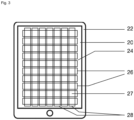
- Area sensors in particular include at least one active circuit, which is preferably referred to as a touch controller, which can be connected to a structure of electrodes.
- this electrode structure is preferably also referred to as an “electrode grid”.
- Area sensors are known in the prior art, the electrodes of which comprise groups of electrodes that differ from one another in their function, for example. These can be, for example, transmitting and receiving electrodes, which can be arranged in a particularly preferred arrangement in the form of columns and rows, that is to say in particular form nodes or intersections at which at least one transmitting and one receiving electrode cross each other or overlap.
- the crossing transmitting and receiving electrodes in the area of the nodes are aligned with one another in such a way that they essentially enclose a 90° angle with one another.
- an electrostatic field that reacts sensitively to changes is formed between the transmitting and receiving electrodes of the surface sensor.
- These changes can occur, for example, by touching the surface of the area sensor with a finger or a conductive object, by touching a contact or grip surface of an electrically conductive structure that is at least partially located on the area sensor, or in particular by bringing the area sensor into contact with an electrically conductive structure, which is arranged, for example, on the underside of a device.
- such changes lead to potential changes within the electrostatic field, which are preferably caused by the electric field between transmitting and receiving electrodes being locally reduced, for example by touching a contact surface of an electrically conductive structure.
- Such a change in the potential conditions is detected and further processed by the electronics of the touch controller.
- the touch controller preferably controls the electrodes in such a way that a signal is transmitted between one or more transmitting electrodes and one or more receiving electrodes, which is preferably an electrical signal, for example a voltage, a current strength or a potential (difference) can act.
- a signal is transmitted between one or more transmitting electrodes and one or more receiving electrodes, which is preferably an electrical signal, for example a voltage, a current strength or a potential (difference) can act.
- These electrical signals in a capacitive surface sensor are preferably evaluated by the touch controller and processed for the device's operating system.
- the information transmitted from the touch controller to the operating system describes so-called individual “touches” or “touch events”, which can be imagined as individual recognized touches or can be described as individual inputs.
- These touches are preferably characterized by the parameters “x coordinate of the touch”, “y coordinate of the touch”, “time stamp of the touch” and “type of touch”.
- the “x and y coordinate” parameters describe the position of the input on the touchscreen. Each pair of coordinates is preferably assigned a time stamp that describes when the entry took place at the corresponding location.
- the “Touch event type” parameter describes the detected state of the input on the touchscreen.
- the types Touch Start, Touch Move, Touch End and Touch Cancel are known to those skilled in the art. With the help of the parameters Touch Start, at least one Touch Move and Touch End as well as the associated coordinates and time stamps, a touch input can be described on the capacitive surface sensor. It is preferred and known in the prior art as multi-touch technology that multiple touch inputs can be evaluated at the same time.
- the periodic signal preferably comprises a number of such touches or touch inputs, with properties of the signal preferably depending on the specific shape of the electrically conductive structure, as well as on the structural arrangement of the transmitting and receiving electrodes of the surface sensor.
- the periodic signal is formed by a set of touches and/or touch inputs that have recurring properties and/or periodicity in spatial and/or temporal terms.
- the course of the periodic signal is determined by the electrically conductive structure.
- Projected capacitance touch technology PCT is an exemplary technology that allows multi-touch operation.
- the amount of touch events or touches is preferably processed and evaluated with the help of a software program ('app').
- the evaluation can include several steps.
- the device parameters of the device containing the area sensor for example the resolution of the touchscreen, are first determined.
- the signal comprising a number of touch events is preferably pre-filtered in the next step and specific characteristics of the signal are amplified or adjusted.
- the signal is then checked for plausibility by calculating parameters such as the time course of the signal, speed and data density, checking for possible manipulation and comparing them with known threshold values.
- various characteristic values and parameters of the signal are then determined or calculated, including the characteristic values start of the signal, end of the signal, local maxima and minima, local velocities of the signal, deflection, amplitudes, period length of periodic signals and possibly others Features to convert the signal into a comparable data set. It is particularly preferred to then compare this data set with other data sets and to assign it to a known data set, for example in a database, and thus to decode the signal. In a further preferred embodiment, the data set is compared using a machine learning model ( artificial neural networks ) previously created from recordings. It was particularly surprising that the use of a machine learning model to decode the signal is particularly suitable for complex signals with many different parameters.
- the decoding of the signal preferably includes an assignment of the detected periodic signal to a known electrically conductive structure or an identification code represented thereby.
- the periodic signal generated by the relative movement of the electrical structure on the surface sensor is particularly tamper-proof. Imitation of the complex periodic signal with another electrically conductive structure (i.e. without presenting the identification code) is almost impossible.
- the device or the system is therefore particularly suitable for authentication procedures, for example to grant a user access to information or an action when the device is placed on a mobile terminal and the movement according to the invention is carried out via the surface sensor.
- the term “capacitive surface sensor” preferably refers to devices having touch sensors that are able to perceive external influences or influences, for example contacts, on the surface of the touch sensor and to evaluate them using attached logic. Such area sensors are used, for example, to make machines easier to operate. In addition to touch sensors, which are primarily used for input, there are touchscreens that are also display and/or output devices. In order to make an input on a capacitive screen, which is also preferably referred to as a touch screen, touch screen or surface sensor, special input pens or similar devices can be used in addition to the fingers. For the purposes of the invention, fingers and special input pens are preferably summarized under the term input means. These are preferably able to change an electrostatic field between row and column electrodes within the area sensor.
- the capacitive, preferably touch-sensitive screen is preferably set up to detect the position of the finger or stylus.
- Area sensors are usually provided in an electronic device, which can be smartphones, cell phones, displays, tablet PCs, tablet notebooks, touchpad devices, graphics tablets, televisions, PDAs, MP3 players, trackpads and/or capacitive input devices, without being limited to that.
- device containing an area sensor or “device with an area sensor” preferably refers to electronic devices, such as those mentioned above, which are able to further evaluate the information provided by the capacitive area sensor. In preferred embodiments, these are mobile devices.
- Touch screens are also preferably referred to as touch screens, surface sensors or touch screens.
- An area sensor does not necessarily have to be used in conjunction with a display or touchscreen.
- the area sensor is integrated visibly or non-visibly in devices, objects and/or devices.
- the electrically conductive structure in the context of the present invention does not have to be activated by a user by touching a portion of the structure, but that the surface sensor also detects the device or its electrically conductive structure in this way, that is, without touching it and/or or activation.
- the invention represents a significant deviation from the known state of the art, since experts had previously assumed that activation of an electrically conductive structure, for example by touching a user, was required in order to be recognized by the capacitive surface sensor.
- the present invention now discloses a device and a system in which an input means for generating a periodic signal can surprisingly be dispensed with.
- the surface sensor is enabled to detect the electrically conductive structure of the device without the structure being activated by a user touch is advantageously based on a coupling between the capacitive surface sensor and the electrically conductive structure, which exists in particular when the electrically conductive structure with at least two rows and at least two columns, or at least two transmitting electrodes and at least two receiving electrodes, of the electrode grid of the capacitive surface sensor interacts.
- the electrically conductive structure overlaps with at least two electrode intersections. An exchange of charge carriers can then occur between the surface sensor, or its electrodes, and the electrically conductive structure.
- the electrically conductive structure on the three-dimensional object causes the electrodes of the electrode grid in the surface sensor to interact with one another indirectly via the electrically conductive structure.
- the electrically conductive structure is designed to bridge a distance between the at least two transmitting and receiving electrodes. In this way, a capacitive connection is preferably created between at least two different electrode intersections, which is produced and held in particular by the electrically conductive structure.
- the electrically conductive structure connects the columns and rows of the electrode grid of the surface sensor with one another, so that an interaction between the at least four affected electrodes (two transmitting electrodes and two receiving electrodes) is caused here.
- the electrically conductive structure is designed to bring about bridging and/or connections of electrode crossings within the electrode grid of the surface sensor.
- the connection and/or bridging of the electrode crossings is preferably based on a capacitive interaction, which is also referred to as capacitive coupling.
- the connection and/or bridging is not based on a galvanic connection, but on a capacitive connection. This can advantageously lead to a self-induced signal generation, in particular to a generation of the desired periodic signal when the device moves via the capacitive surface sensor.
- the electrically conductive structure comprises at least one main element. In a further preferred embodiment, the electrically conductive structure comprises at least one sub-element in addition to the main element. Main element and one or more sub-elements are galvanically connected to one another and form the electrically conductive structure as a whole.
- the electrically conductive structure can be characterized by the design of the main element and the design of the sub-elements. For the purposes of the invention, the term design includes, but is not limited to, the shape, size, geometry, length, width, orientation, position and angle of the element of the electrically conductive structure.
- Main and/or sub-elements can be, for example, linear, circular or arcuate without being limited to this.
- the transition between the sub-element and the main element can also be flowing or arcuate. It may also be preferred to electrically connect a sub-element to another sub-element instead of the sub-element.
- the number, arrangement and orientation of the sub-elements is not limited to the variants described.
- the entirety of the main and sub-elements that are galvanically connected to one another is referred to as an electrically conductive structure. It can also be preferred that there are two or more electrically conductive structures on a contact surface of the object, which are characterized in that they are not galvanically connected to one another.
- the electrically conductive structure interacts with the electrode grid of the capacitive area sensor.
- different electrode crossings interact with the electrically conductive structure or one or more centroids of the electrically conductive structure.
- An electrode crossing interacts with the electrically conductive structure in particular when the electrically conductive structure overlaps selected electrode crossings at a time x.
- the center of gravity of the electrically conductive structure interacts with the capacitive surface sensor or the electrode grid. At points where the center of gravity of the electrically conductive structure overlaps with the electrode intersections, the capacitive surface sensor is activated or, in other words, a touch event is generated.
- the electrically conductive structure or the center of gravity gradually interacts with other electrode intersections. This results in a superposition of two different geometries: on the one hand, the geometry of the electrode grid and, on the other hand, the geometry of the electrically conductive structure. If these two geometries are moved relative to each other, the two geometries overlap. This overlay repeats itself cyclically or periodically. This leads to periodically arranged touch events on the capacitive surface sensor, which then form the periodic signal as a whole. Similar effects are known to experts in optics under the term interference. It was completely surprising that an electrically conductive structure enters into such an interaction with the capacitive surface sensor.
- the electrically conductive structure interacts with at least two rows and at least two columns at all times of movement. It is particularly preferred that the two columns and/or two rows are not adjacent. In other words, it is preferred that the electrically conductive structure connects or bridges two spaced-apart rows and/or two spaced-apart columns.
- this connection between different electrode crossings or the transmitting and receiving electrodes of the electrode grid makes the activation of the electrically conductive structure by the touch of a user obsolete, so that in the context of the present invention, surprisingly, the use of one Input means, such as a user's finger, can be dispensed with.
- the advantageous effects and technical effects of the invention are preferably based on the interaction between the electrically conductive structure and the surface sensor, particularly preferably between the electrically conductive structure and the electrode grid of the surface sensor and most preferably between the electrically conductive structure and the columns and rows or the Transmitting and receiving electrodes of the electrode grid of the surface sensor.
- this interaction preferably leads to a change in the electrostatic field between the electrodes in a surface sensor and/or to a measurable change in the capacitance.
- the change in the electrostatic field can be brought about in particular by a relative movement between the surface sensor and the three-dimensional object.
- the periodic signal is generated by a relative movement between the electrically conductive structure and the surface sensor.
- this relative movement can preferably also be referred to as a dynamic active contact.
- the duration of the relative movement determines the duration of the periodic signal.
- duration means in particular the total duration of the signal.
- the periodic signal has a duration of at least 250 ms, preferably at least 500 ms and particularly preferably at least 750 ms.
- the present invention also departs from the prior art in that a touch structure on the device is no longer required to generate a signal on the area sensor.
- a touch structure requires a specific spatial structure of predefined elements of an electrically conductive structure, namely in particular a touch point, a coupling surface and line means for connection.
- the presence of these predefined elements and their functionalities is not required in the context of the present invention, nor is the need to recreate or imitate the properties of fingertips with the electrically conductive structure.
- the proposed device does not require a special coupling surface that must be touched by a user in order to activate the electrically conductive structure for the surface sensor.
- Area sensors are usually provided in an electrical device, which can be smartphones, cell phones, displays, tablet PCs, tablet notebooks, touchpad devices, graphics tablets, televisions, PDAs, MP3 players, trackpads and/or capacitive input devices, without being limited to that.
- Touch screens are also preferably referred to as touch screens, surface sensors or touch screens.
- An area sensor does not necessarily have to be used in conjunction with a display or touchscreen.
- the area sensor is integrated visibly or non-visibly in devices, objects and/or devices.
- Such surface sensors are preferably set up to detect multiple touches at the same time, which means, for example, that elements displayed on a touchscreen can be rotated or scaled using special gestures.
- the electrically conductive structure is set up to determine a course of the periodic signal with regard to a curve course, an amplitude and/or an edge course.
- the design of the electrically conductive structure determines the course of the periodic signal, in particular the curve course, the amplitudes and/or the edge course.
- the term “curve progression” preferably describes the graphical representation or reproduction of the x(y) function in the coordinate system, which can be mentally placed over the screen of the surface sensor.
- the term describes the course of the x(y) function in the virtual coordinate system.
- the term “amplitude” preferably describes the maximum deviation from a fixed center position around which the periodic signal can fluctuate.
- the amplitude of the signal is at least 1 mm so that the amplitude of the periodic signal can be evaluated when evaluating the amount of touch signals or touch events.
- the amplitude is preferably at least 2 mm and particularly preferably at least 3 mm.
- the amplitude of the periodic signal is a maximum of 60 mm, since this corresponds to the approximate maximum width of today's capacitive area sensors in mobile phones or smartphones.
- the amplitude of the periodic signal is particularly preferably a maximum of 40 mm, since a corresponding periodic signal can be evaluated particularly well. Surprisingly, a corresponding signal can be evaluated particularly well in combination with another periodic signal.
- edge profile preferably describes the profile of the signal in more detail and includes, but is not limited to, the variables rise, fall and edge steepness.
- the electrically conductive structure is designed to determine a periodic non-harmonic signal.
- Non-harmonic signals can preferably be represented from an overlap of several harmonic signals. In other words, the appearance of the signal can also be described as fidgeting, shaking or shaking.
- the location-dependent signal has a loop-shaped course.
- the electrically conductive structure is set up so that the coordinate of the signal, in the direction of which the device is moved via the capacitive surface sensor, periodically increases and decreases, i.e. the signal partially runs backwards relative to the direction of movement of the electrically conductive structure.
- the course on the capacitive surface sensor can be displayed as a loop or I-shaped course (small cursive L) of the signal.
- the electrically conductive structure is present both on the contact surface, ie on the surface of the device that is intended for effective contact with the surface sensor, and on at least one further surface of the device.
- electrically conductive structure is present both on the underside, which serves as a contact surface, and on at least one side surface of the device. This feature is essentially equivalent to the statement that at least part of the electrically conductive structure is suitable for interacting with the electrode grid of the capacitive area sensor.
- the part of the electrically conductive structure that interacts with the surface sensor is preferably the part of the electrically conductive structure that is arranged on the contact surface of the three-dimensional object.
- At least part of the electrically conductive structure is present on the contact surface of the three-dimensional object, while in preferred embodiments of the invention it may also be preferred that, in addition to the parts of the electrically conductive structure that are present on the contact surface of the device, there are further parts of the electrically conductive Structure present on the adjacent surfaces of the device. It can therefore be preferred in the sense of the invention that essentially the entire electrically conductive structure is present on the contact surface of the three-dimensional object or only a portion of the electrically conductive structure.
- the corresponding device is particularly easy to manufacture since only one side of the three-dimensional object needs to be printed or provided with electrically conductive material.
- This feature is essentially equivalent to the statement that the entire electrically conductive structure is suitable for interacting with the electrode grid of the capacitive area sensor.
- this embodiment of the invention avoids difficulties that can arise, for example, if an element of the electrically conductive structure is present on two sides of the object, in the sense that this element then has to extend over one edge of the object.
- a disadvantage in the prior art is the need for the electrically conductive structure to be guided over one or more edges of a three-dimensional object.
- edges of the object are exposed to greater mechanical stress than, for example, the inner surfaces of the side surfaces or the underside of the object.
- strong mechanical loads occur, particularly in the area of the edges of the folding box.
- This can lead to a reduction in electrical conductivity or even breakage of the electrically conductive structure.
- the arrangement of the electrically conductive structure exclusively on one side of the object therefore represents a decisive advantage over the solutions known from the prior art.
- the electrically conductive structure is designed to interact with at least two rows and at least two columns of an electrode grid of the capacitive surface sensor.
- the invention prefers that the rows of the electrode grid of the area sensor are essentially formed by transmitting electrodes and the columns of the electrode grid of the area sensor are essentially formed by receiving electrodes, or vice versa.
- the columns of the electrode grid of the surface sensor comprise either only transmitting electrodes or only receiving electrodes. It is further preferred that the rows of the electrode grid of the surface sensor are also formed by either only transmitting electrodes or only by receiving electrodes.
- the electrically conductive structure of the three-dimensional object is set up to interact with at least two receiving electrodes and at least two transmitting electrodes of the electrode grid of the capacitive surface sensor. It may be preferred that there are two transmitting and receiving electrodes located next to each other. In a further embodiment, it may also be particularly preferred that the transmitting and/or receiving electrodes are spaced apart, that is to say that there are further electrodes between the electrodes that interact.
- the transmitting electrodes which are preferably arranged next to one another, are arranged essentially parallel to one another. It is also preferred that the receiving electrodes, which are preferably arranged next to one another, are arranged essentially parallel to one another.
- the receiving electrodes of the electrode grid of the surface sensor are arranged essentially perpendicular to the transmitting electrodes of the electrode grid, the term "substantially” not being unclear to the average person skilled in the art because the average person skilled in the art knows how the term is used can be understood in practice.
- the person skilled in the art also knows in particular that, for example, slight deviations from exact parallelism or orthogonality can arise due to manufacturing reasons. For the purposes of the invention, such deviations should also be encompassed by the phrases “essentially parallel” and “essentially perpendicular”.
- a pattern similar to a checkered pattern results between two transmitting and receiving electrodes, which are preferably located next to one another.
- the electrically conductive structure interacts with at least two rows and at least two columns, or at least two transmitting electrodes and at least two receiving electrodes, of the electrode grid of the capacitive surface sensor. It has surprisingly been found that the course of the periodic signal is determined by the interaction of partial areas of the electrically conductive structure with the electrode grid of the capacitive surface sensor, this determination of the periodic signal in particular by the interaction between the specific design of the electrically conductive structure with the at least two transmitting and receiving electrodes is achieved.
- the invention in a further aspect, relates to a system for generating a periodic signal on a capacitive surface sensor, the system comprising a device and a capacitive surface sensor.
- the system is characterized in that the periodic signal is generated on the capacitive surface sensor by a relative movement between the electrically conductive structure and the surface sensor.
- the electrically conductive structure on the device is set up to determine the course of the periodic signal in interaction with the electrode grid of the capacitive surface sensor.
- the electrically conductive structure is set up in such a way that when the device moves relative to the surface sensor along the direction of a row or a column of the electrode grid, a periodic signal is generated which oscillates orthogonally to the movement of the device.
- the proposed system comprises a device, which is preferably a three-dimensional object, and a capacitive surface sensor, which is preferably referred to as a “surface sensor” for short in the sense of the invention.
- the course of the periodic signal is preferably determined by the design of the electrically conductive structure on the device, while the period length of the periodic signal is determined by the design of the surface sensor, in particular its electrode grid of transmitting and receiving electrodes.
- the period length of the periodic signal is determined by the geometry of the electrode grid in the capacitive surface sensor.
- the arrangement and/or design of the electrode grid of the surface sensor can preferably also be referred to as the “geometry of the electrode grid”.
- the duration of the interaction between the electrically conductive structure and the surface sensor determines the duration of the periodic signal.
- the duration of the periodic signal means in particular the total duration of the periodic signal.
- the periodic signal has a duration of at least 250 ms, since a minimum duration of the periodic signal is required so that the characteristic values of the signal can be evaluated accordingly.
- the duration of the periodic signal is particularly preferably at least 500 ms, since a larger number of touch data or touch events are available for evaluation and mean values over the key figures, for example Amplitude of the signal can be formed.
- the periodic signal has a particularly preferred minimum duration of at least 750 ms.
- the proposed system thus provides the possibility of generating a periodic signal on a surface sensor by moving a device, in particular a three-dimensional object, over the surface sensor.
- a device in particular a three-dimensional object
- the conscious and intentional generation of periodic signals through a specific configuration or design of an electrically conductive structure on a device or through a specific configuration or geometry of the electrode grid of a surface sensor has not yet been described in the prior art.
- the properties of the periodic signal to be generated can be consciously influenced, varied and/or changed through the specific design or influence and/or change on the structural design of the electrically conductive structure and/or the electrode grid.
- the properties of the periodic signal that can be set in this way are preferably the spatial and/or temporal properties of the periodic signal, for example its amplitude or period length or period length.
- the spatial and/or temporal properties of a periodic signal can be influenced by providing a system comprising a device with an electrically conductive structure and an area sensor. It was completely surprising that the invention can provide a particularly intuitive and user-friendly interactive system, with the help of which an object or its user can be verified and/or identified particularly safely and clearly using a capacitive surface sensor.
- the proposed device and the proposed system are particularly secure against manipulation and the corresponding electrically conductive structure in particular cannot be imitated by fingertips or manipulated by a user.
- the term “identification” preferably means that a device or an object is recognized by the area sensor and can, for example, be assigned to a data record stored in the electrical device that contains the area sensor.
- the data record may not be stored directly in the electrical device, but may be accessible to it, for example by being retrievable on a server, on the Internet and/or in a cloud.
- the detection of the object by the surface sensor takes place in particular by detecting the electrically conductive structure that is arranged on the object. This electrically conductive structure is determined in particular by the design of the entire electrically conductive structure and/or its subregions.
- the term “verification” preferably means that the authenticity or authenticity of an object can be determined or proven.
- Holograms for example, have long been known in the prior art. However, it is often only possible for experts to check or prove the authenticity of a hologram. It was completely surprising that with the present invention an unequivocal verification of the feature in the form of the electrically conductive structure can be carried out using a device which contains an area sensor, for example a smartphone. Areas of application for such an application are in the area of product and document protection.
- the electrically conductive structure on an object serves as an access key to digital content.
- the electrically conductive feature serves as a key for unlocking digital content, such as guarantee certificates, vouchers, coupons, digital media, etc.
- the periodic signal is generated on the capacitive surface sensor by a relative movement between the electrically conductive structure and the surface sensor.
- the device or the object is preferably set up to generate such a periodic signal on a capacitive surface sensor, the periodic signal being generated in particular by a relative movement between the electrically conductive structure and the surface sensor.
- this preferably means that the device and the surface sensor are displaced relative to one another, so that a movement of the two objects relative to one another is caused. This can be done, for example, by moving the object on or across the screen of an area sensor.
- the device or its contact surface preferably rests on the screen of the surface sensor.
- the device is pulled over the surface sensor in order to obtain a relative movement with which the periodic signal is generated on the surface sensor. This pulling or pushing movement is preferably referred to as relative movement.
- duration of the relative movement determines the duration of the periodic signal.
- duration means in particular the total duration of the signal.
- the periodic signal has a duration of at least 250 ms, preferably at least 500 ms and particularly preferably at least 750 ms.
- the system according to the invention is preferably set up to detect and evaluate the described generation of a periodic signal in order to identify or verify the applied electrical structure.
- the system has a data processing device which is set up to evaluate the periodic signal, with software ('app') preferably installed on the data processing device, which includes commands to determine dynamic characteristic values of the periodic signal and with reference data to compare.
- the device containing the area sensor has a data processing device which is set up to evaluate the periodic signal, with software ('app') preferably installed on the data processing device, which includes commands to determine dynamic characteristic values of the periodic signal and compare with reference data.
- the software is at least partially provided in the form of a cloud service or Internet service, with the device transmitting the touch data or touch events via the Internet to an application in the cloud.
- a cloud service or Internet service there is software ('app') on a data processing device, which includes commands to determine dynamic characteristic values of the periodic signal and compare them with reference data.
- the software installed on the device's data processing device does not carry out all computationally intensive steps independently on the device. Instead, the data about the periodic signal or the set of touch events is transmitted to a software application in a cloud (with an external data processing device) to determine dynamic characteristic values and compare them with reference data.
- the software as a cloud service which preferably includes commands to determine dynamic characteristics of the periodic signal and compare them with reference data, processes the periodic signal in the form of a set of touch events and sends the result back to the device comprising the area sensor or to the software installed on it.
- the software on the device can preferably further process the results and, for example, control their display.
- the person skilled in the art will recognize that these preferably apply equally to software that carries out the steps entirely on the device as well as to software that performs some (preferably computationally intensive) steps, such as determining dynamic Parameters and their comparison with reference data have been outsourced to an external data processing device of a cloud service.
- some (preferably computationally intensive) steps such as determining dynamic Parameters and their comparison with reference data have been outsourced to an external data processing device of a cloud service.
- the intended evaluation of the periodic signal is to be understood as a unified concept, regardless of which steps of the algorithm are carried out on the device itself or by an external data processing device on a cloud.
- the dynamic characteristics of the periodic signal can also be determined by the software on the device and only the comparison of the dynamic parameters with reference data is carried out outsourced to a cloud service.
- the device containing the area sensor is preferably an electronic device which is able to further evaluate the information provided by the capacitive area sensor.
- the capacitive surface sensor or the device preferably has an active circuit, also called a touch controller, which allows evaluation of touch signals on the surface sensor as described above.
- the touch controller and an operating system provided on the electronic device the periodic signal is preferably prepared as a set of touch events.
- a touch event preferably refers to a software event that is provided by the operating system of the device with the capacitive surface sensor when an electronic parameter detected by the touch controller changes.
- An operating system preferably refers to the software that communicates with the hardware of the device, in particular the capacitive surface sensor or the touch controller, and enables other programs, such as the software ('app'), to run on the device.
- Examples of operating systems for devices with capacitive surface sensors are Apple's iOS for iPhone, iPad and iPod Touch or Android for operating various smartphones, tablet computers or media players.
- Operating systems control and monitor the hardware of the device, in particular the capacitive surface sensor or a touch controller.
- operating systems for the system in question provide a set of touch events that reflect the periodic signal.
- a touch start, a touch move and touch end can be detected at different positions, whereby the time sequence can be traced using the x or y coordinates and the time stamp of the touches.
- the relative movement of the device preferably causes alternating generation of touch events, which, as described, reflects the periodicity of the electrode grid.
- the periodic signal is preferably processed by the operating system or the touch controller of the electronic device, such as a smartphone.
- the software ('app') installed on the data processing device preferably evaluates the periodic signal based on the detected number of touch events.
- the data processing device is preferably a unit which is suitable and configured for receiving, sending, storing and/or processing data, preferably touch events.
- the data processing unit preferably comprises an integrated circuit, a processor, a processor chip, a microprocessor and/or microcontroller for processing data, as well as a data memory, for example a hard drive, a random access memory (RAM), a read-only memory (ROM) or also a flash memory to store the data.
- a data memory for example a hard drive, a random access memory (RAM), a read-only memory (ROM) or also a flash memory to store the data.
- Corresponding data processing devices are available in commercially available electronic devices with area sensors, such as mobile devices or smart devices.
- the software can be written in any programming language or model-based development environment, such as C/C++, C#, Objective-C, Java, Basic/VisualBasic or Kotlin.
- the computer code may include subprograms written in a proprietary computer language that are specifically intended for reading or controlling or another hardware component of the device.
- the software preferably determines dynamic characteristics of the periodic signal (preferably in the form of a set of touch events) in order to compare these reference data.
- Dynamic characteristics of the periodic signal are, for example, the period length, the curve shape, the amplitude and/or the edge curve.
- the dynamic characteristic values can be, for example, start, end, local maxima, local minima, local velocities, deflection and/or amplitudes of touch events or a set of touch events.
- the entirety of the dynamic characteristics that characterize the periodic signal can preferably be summarized in a data set, which can be compared with a reference data set in order to identify or verify the applied electrical structure.
- the data set is compared using a machine learning model ( artificial neural networks ) previously created from recordings or calibration data.
- reference data can be generated for this purpose by placing the device with a known electrical structure on a surface sensor and moving it in the direction of a row or column of the surface sensor.
- reference data preferably includes threshold values or reference data sets.
- reference data preferably refers to all data that allows an assignment of a detected periodic signal to an identification code or a known electrical structure.
- the reference data can preferably be stored on a computer-usable or computer-readable medium on the data processing unit. Any file format used in the industry may be suitable.
- the reference data can be stored in a separate file and/or integrated into the software (e.g. in the source code).
- the identification methods known in the prior art are based in particular on the detection of static signals of an electrical structure, for example a touch structure, which imitates the touch of fingertips. With sufficient skill, it is in principle possible to recreate such touch structures with the fingers using the known methods or systems.
- a simulation of a periodic signal generated according to the invention is not possible without providing an identical electrical structure. Even if it were possible to simulate the generation of initial touch events at a time by cleverly placing fingers or other capacitive structures, it would not be possible to move the fingers in such a way that a periodic signal could be generated.
- the fingers would be recognized as a touch move if they remained in contact and their signals would not oscillate back and forth in correlation with the periodicity of the electrode grid.
- the software can also carry out a series of plausibility checks to rule out manipulation of the signal.
- the software evaluates the time course of the periodic signal and compares it with reference data in order to estimate the probability that guiding a structure using the input signal leads to the detected time course of the dynamic signals.
- the software can evaluate dynamic characteristics of the periodic signal, such as its period length, amplitude and/or period duration, and compare them with reference data.
- the period length, amplitude and/or period duration are particularly suitable parameters for characterizing the periodic signals and the electrical structure on which they are based.
- the period length should, for example, preferably correlate with the lattice constants of the electrode grid.
- the determination of the dynamic characteristic values of the periodic signal and the comparison with threshold values and/or reference data sets thus preferably allows both a check of the plausibility of the signal and its assignment to reference data for identification purposes.
- the evaluation using the software can be implemented in different ways and includes several steps.
- the device parameters of the device containing the area sensor e.g. the resolution of the area sensor or touchscreen, can first be determined.
- the periodic signal comprising a number of touch events is preferably pre-filtered and specific characteristics of the signal are amplified or adapted.
- the software is therefore not limited to a specific type of device, but can deliver optimal results for different electronic devices.
- the signal After filtering the periodic signal, the signal can be checked for plausibility by calculating parameters such as the time course of the signal, speed and data density. Based on a comparison with known or calibrated threshold values, any manipulation can be reliably ruled out.
- the characteristic values start of the signal, end of the signal, local maxima and minima, local velocities of the signal, deflection, amplitudes, period length of periodic signals can be determined and, if necessary, converted into a data record with further features surrounding the periodic signal.
- the dynamic parameters should be particularly suitable for characterizing the oscillation of the periodically generated touch events.
- the data set obtained can then be compared with a reference data set, which is, for example, in a database, in order to decode the periodic signal, whereby a machine learning algorithm can preferably be used.
- Decoding preferably means an assignment of the periodic signal to a known identification code or a known electrically conductive structure.
- the kit may also include instructions for moving the device relative to the area sensor along the direction of a row or column to generate a periodic signal that oscillates orthogonally to the movement of the device.
- the invention relates to the use of the proposed device for generating a periodic signal on a capacitive surface sensor with an electrode grid comprising rows and columns, the electrically conductive structure of the device being brought into operative contact with the capacitive surface sensor and the device along a row or column of the electrode grid is moved relative to the capacitive surface sensor.
- the electrically conductive structure be applied to a substrate material using foil transfer methods, for example cold foil transfer, hot stamping and/or thermal transfer, without being limited to these application methods.
- foil transfer methods for example cold foil transfer, hot stamping and/or thermal transfer
- printing methods such as offset printing, gravure printing, flexographic printing, screen printing and/or inkjet methods can be used to produce the electrically conductive structure on the non-conductive substrate without being limited to this.
- Suitable electrically conductive inks include materials based, for example, on metal particles, nanoparticles, carbon, graphene and/or electrically conductive polymers, but are not limited to these materials.
- the electrically conductive structure may also be preferred to cover the electrically conductive structure by at least one further layer, whereby this layer can be a paper- or film-based laminate material or at least one lacquer/paint layer.
- This layer can be optically transparent or opaque.
- the electrically conductive structure is applied to the inside of a side surface of the object, for example on the inside of the contact surface or underside of a folding box.
- a feature of classic conventional printing processes is the simple and quick reproduction of a motif by applying the motif to be printed to a printing form, for example a gravure cylinder or an offset printing plate, and then reproducing it multiple times and at high speed.
- Conventional printing processes are not suitable for producing individualized content because printing form production represents a significant proportion of the overall production costs. This means that only larger runs of a printed product can be produced economically.
- graphic printing digital printing processes exist for the production of small runs and individualized products with which individual content can be printed economically. These printing processes include, for example, electrophotography, laser printing or inkjet printing. It is also possible to produce individualized electrically conductive structures using process combinations of conventional printing processes and additive or subtractive processes.
- the periodic signals (40) are shown as if they had been recorded on the capacitive surface sensor (20) over the period of the relative movement (30) of the device (10), i.e. the touch inputs on the capacitive surface sensor (20) were recognized, recorded and displayed on the touchscreen.
- this signal displayed on the touchscreen is referred to as the “recorded periodic signal” (40).
- the signal (40) gradually arises during the relative movement (30) of the device (10) via the capacitive surface sensor (20). As soon as the device (10) has been moved over an area of the surface sensor (20), a signal (40) can no longer be detected at this point, i.e. the touchscreen is no longer “activated” at this point.
- Figure 2 shows the recorded periodic signal (40) on the capacitive surface sensor (20), which is part of an electronic device (22).
- the periodic signal (40) is characterized by the period length (42) and the amplitude (44).
- the period length (42) is the smallest local interval after which the process repeats itself.
- the amplitude (44) is the maximum deflection of the periodic signal (40) from the position of the arithmetic mean value of the signal.
- Figure 3 shows the electronic device (22), which contains the capacitive surface sensor (20).
- the surface sensor (20) has an electrode grid (24) which comprises rows (26) and columns (28).
- Rows (26) and columns (28) generally represent transmitting and receiving electrodes of the capacitive area sensor (20).
- Figure 4 shows a preferred embodiment of the electrically conductive structure (12).
- the electrically conductive structure (12) can be characterized by the design of the main element (16) and the design of the sub-elements (18).
- the term design includes, but is not limited to, the shape, size, geometry, length, width, orientation, position and angle of the elements of the electrically conductive structure (12).
- the main element (16) for example, has a linear shape with a length of 45 mm and a width of 2 mm.
- the main element (16) is present on the device (not shown) at an angle of 20°.
- the left sub-element (18) is also linear, has a length of 13 mm and a width of 2 mm and is at an angle of 40°.
- the right sub-element (18) is also linear, has a length of 6 mm and a width of 2 mm and is at an angle of 70°. Both sub-elements (18) are galvanically connected to the main element (16) and, together with the main element (16), form the electrically conductive structure (12) as a whole.
- FIG. 5 The left shows the device (10) comprising an electrically conductive structure (12) on the capacitive surface sensor (20).
- the electrically conductive structure (12) interacts with the electrode grid (24) of the capacitive area sensor (20).
- the electrode crossings (27), which interact with the electrically conductive structure (12) are shown hatched. If the device (10) comprising the electrically conductive structure (12) is moved over the electrode grid (24) of the capacitive surface sensor (20), the electrically conductive structure (12) gradually interacts with other electrode crossings (27). It is preferred that the electrically conductive structure (12) interacts with at least two rows (26) and at least two columns (28) at any time of movement (30).
- Figure 6 shows a preferred embodiment of the electrically conductive structure (12), arranged on the electrode grid (24) of the capacitive surface sensor (shown only as a section).
- the touch events (46) generated by the electrically conductive structure (12) are shown by dashed circles at the corresponding electrode intersections (27).
- the electrically conductive structure (12) bridges a distance between two electrode intersections (27).
- the electrically conductive structure (12) connects the columns (28) and rows (26) of the electrode grid (24) of the surface sensor (20) to one another, so that there is an interaction between the at least four affected electrodes (two transmitting electrodes and two receiving electrodes). The interaction between the electrodes is shown by arrows.
- Figure 7 shows different states when moving the device (10) comprising the electrically conductive structure (12) via the capacitive surface sensor (20) or the electrode grid (24).
- the lines (26) of the electrode grid (24) are numbered. A total of 5 states are shown t1, t2, t3, ..., tx and tx+1.
- the arrow indicates the movement of the device (10) or the electrically conductive structure (12) relative to the electrode grid (24).
- the touch events (46) generated at the respective time are shown by dashed circles on the respective individual graphics.
- the touch events generated at a previous point in time are shown with simple circles. The circles were connected with lines to illustrate the timing.
- a touch event (46) is generated when the respective electrode intersection (27) of the underlying electrode grid (24) is covered or overlapped by a minimum area of the electrically conductive structure (12). This minimum area is preferably >20% of the area of an electrode intersection and particularly preferably >30% of the area of an electrode intersection.
- Figure 8 shows the device (10) in the form of a three-dimensional object on a capacitive surface sensor (20), which is part of an electronic device (22).
- the device (10) comprises an electrically conductive structure (12) which is arranged on the underside or contact side (50) and on two side surfaces (52) of the object. This portion of the electrically conductive structure (12) can be referred to as a contact surface or gripping surface.
- Figure 9 shows further embodiments of the electrically conductive structure (12), which differ in particular with regard to the design of the main element (16) and the sub-elements (18).
- the electrically conductive structure (12) can consist of two separate areas.
- the periodic signals (40) generated in this way on the capacitive surface sensor (20) are correspondingly more complex.
- the number, arrangement and orientation of the main elements (16) and partial elements (18) are not limited to the variants shown.
- the steps of processing and evaluating the touch events or touches are shown with the help of a software program.
- the device parameters of the device containing the area sensor for example the resolution of the touchscreen, are first determined.
- the signal comprising a number of touch events is preferably pre-filtered in the next step and specific characteristics of the signal are amplified or adapted.
- the signal is then checked for plausibility by calculating parameters such as the time course of the signal, speed and data density, checking for possible manipulation and comparing them with known threshold values.
- various characteristic values and parameters of the signal are then determined or calculated, including the characteristic values start of the signal, end of the signal, local maxima and minima, local velocities of the signal, deflection, amplitudes, period length of periodic signals and possibly others Features to convert the signal into a comparable data set. It is particularly preferred to then compare this data set with other data sets and to assign it to a known data set, for example in a database, and thus to decode the signal. In a further preferred embodiment, the data set is compared using a machine learning model (artificial neural networks) previously created from recordings. It was particularly surprising that the use of a machine learning model to decode the signal is particularly suitable for complex signals with many different parameters.
- a machine learning model artificial neural networks
Landscapes
- Engineering & Computer Science (AREA)
- General Engineering & Computer Science (AREA)
- Theoretical Computer Science (AREA)
- Human Computer Interaction (AREA)
- Physics & Mathematics (AREA)
- General Physics & Mathematics (AREA)
- Position Input By Displaying (AREA)
Claims (15)
- Système de génération d'un signal périodique (40) sur un capteur superficiel capacitif (20), dans lequel le système comprend un dispositif (10) et un appareil (22) doté d'un capteur superficiel capacitif (20),
dans lequela) le dispositif (10) est un objet tridimensionnel, dans lequel l'objet tridimensionnel présente une surface de contact (50), dans lequel une structure électriquement conductrice (12) est disposée au moins sur la surface de contact (50) de l'objet tridimensionnelb) le capteur superficiel capacitif (20) présente une grille d'électrodes (24) comprenant des rangées (26) et des colonnes (28),caractérisé en ce que la structure électriquement conductrice (12) et le capteur superficiel (20) sont conçus de sorte que lorsque le dispositif (10) se déplace par rapport au capteur superficiel (20) dans la direction d'une rangée (26) ou d'une colonne (28) de la grille d'électrodes (24), un signal périodique (40) est généré, qui oscille orthogonalement au mouvement du dispositif (10). - Système selon la revendication précédente,
caractérisé en ce que
la longueur de période (42) du signal périodique (40) est corrélée à la constante de grille de la grille d'électrodes (24) dans le capteur superficiel capacitif (20). - Système selon la revendication 1 ou 2,
caractérisé en ce que
la longueur de période (42) du signal périodique (40) est d'au moins 2 mm, de préférence d'au moins 3 mm et de manière particulièrement préférée d'au moins 4 mm et/ou de maximum 9 mm, de préférence de maximum 7 mm et de manière particulièrement préférée de maximum 5 mm et/ou l'amplitude (44) du signal périodique (40) est d'au moins 1 mm, de préférence d'au moins 2 mm et de manière particulièrement préférée d'au moins 3 mm et/ou de préférence de maximum 60 mm et de manière particulièrement préférée de maximum 40 mm. - Système selon une ou plusieurs des revendications précédentes,
caractérisé en ce que
la structure électriquement conductrice (12) est conçue pour déterminer une évolution du signal périodique (40) sur le capteur superficiel capacitif (20) en fonction d'une évolution de courbe, d'une amplitude (44) et/ou d'une évolution de flanc. - Système selon une ou plusieurs des revendications précédentes,
caractérisé en ce que
la structure électriquement conductrice (12) est conçue pour être en interaction avec au moins deux rangées (26) et au moins deux colonnes (28) d'une grille d'électrodes (24) du capteur superficiel capacitif (20). - Système selon une ou plusieurs des revendications précédentes,
caractérisé en ce que
la structure électriquement conductrice (12) présente au moins deux zones partielles avec deux centres de gravité superficiels, qui sont conçues pour générer un événement tactile en cas de superposition avec une intersection de la grille d'électrodes (24) et, en cas d'absence de superposition avec une intersection de la grille d'électrodes (24), aucun événement tactile, de sorte que lors d'un déplacement relatif du dispositif (10) le long d'une rangée ou d'une colonne de la grille d'électrodes (24), un signal périodique (40) est généré par génération alternée d'un événement tactile avec superposition alternée du premier ou du second centre de gravité superficiel avec des intersections de la grille d'électrodes. - Système selon une ou plusieurs des revendications précédentes,
caractérisé en ce que
la structure électriquement conductrice (12) présente au moins deux zones partielles qui, en fonction du positionnement sur la grille d'électrodes (24), recouvrent une surface minimale supérieure à 20 %, de préférence supérieure à 30 %, et/ou une surface maximale inférieure à 70 %, de préférence inférieure à 50 % de la superficie d'une intersection d'électrodes sous-jacente. - Système selon une ou plusieurs des revendications précédentes,
caractérisé en ce que
le système comprend un dispositif de traitement de données qui est configuré pour évaluer le signal périodique (40), dans lequel un logiciel (« application ») est de préférence installé sur le dispositif de traitement de données, qui comprend des commandes pour évaluer des caractéristiques dynamiques du signal périodique (40) et les comparer avec des données de référence, dans lequel les caractéristiques dynamiques comprennent de préférence une longueur de période (42), une amplitude (44) et/ou une durée de période. - Système selon la revendication précédente,
caractérisé en ce que
l'appareil (22) contenant le capteur superficiel (20) traite le signal périodique comme un ensemble d'événements tactiles et un logiciel détermine des caractéristiques dynamiques de l'ensemble d'événements tactiles. - Dispositif de génération d'un signal périodique (40) sur un capteur superficiel capacitif (20) doté d'une grille d'électrodes (24) comprenant des rangées (26) et des colonnes (28), dans lequelle dispositif (10) est un objet tridimensionnel, dans lequel l'objet tridimensionnel présente une surface de contact (50), dans lequel une structure électriquement conductrice (12) est disposée au moins sur la surface de contact (50) de l'objet tridimensionnel,caractérisé en ce quela structure électriquement conductrice (12) et un capteur superficiel (20) sont conçus de sorte que lorsque le dispositif (10) se déplace par rapport au capteur superficiel (20) dans la direction d'une rangée (26) ou d'une colonne (28) de la grille d'électrodes (24), un signal périodique (40) est généré, qui oscille orthogonalement au mouvement du dispositif (10) .
- Dispositif selon la revendication précédente
caractérisé en ce que
la structure électriquement conductrice (12) a une forme linéaire dont la largeur est de 0,5 mm à 8 mm, de préférence de 1,5 mm à 5 mm. - Dispositif selon l'une des revendications précédentes 10 ou 11
caractérisé en ce quela structure électriquement conductrice (12) comprend au moins un élément principal linéaire (16) et au moins un élément partiel linéaire (18), dans lequel l'élément principal (16) et l'élément partiel (18) sont reliés galvaniquement l'un à l'autre et de préférence incluent un angle de 10° à 80°, de manière particulièrement préférée de 20° à 60°et/ou dans lequel la surface de contact (50) présente de préférence une forme sensiblement rectangulaire et l'élément principal (16) présente un angle de 5° à 45°, de préférence de 10° à 35°, par rapport à l'un des deux bords de la surface de contact (50). - Utilisation du dispositif (10) selon une ou plusieurs des revendications 10 à 12 pour générer un signal périodique (40) sur un capteur superficiel capacitif (20) doté d'une grille d'électrodes comprenant des rangées (26) et des colonnes (28), caractérisée en que
la structure électriquement conductrice (12) du dispositif (10) est mise en contact efficace avec le capteur superficiel capacitif (20) et le dispositif (10) est déplacé le long d'une rangée ou d'une colonne de la grille d'électrodes (24) par rapport au capteur superficiel capacitif (20). - Kit de génération et d'évaluation d'un signal périodique (40) sur un capteur superficiel capacitif (20) doté d'une grille d'électrodes (24) comportant des rangées (26) et des colonnes (28), comprenanta) un dispositif (10), qui est un objet tridimensionnel, dans lequel l'objet tridimensionnel présente une surface de contact (50), dans lequel une structure électriquement conductrice (12) est disposée au moins sur la surface de contact (50) de l'objet tridimensionnelb) un logiciel (« application ») à installer sur un appareil (22) comprenant le capteur superficiel (20)caractérisé en ce que
la structure électriquement conductrice (12) est conçue de sorte que lorsque le dispositif (10) se déplace par rapport au capteur superficiel (20) dans la direction d'une rangée (26) ou d'une colonne (28) de la grille d'électrodes (24), un signal périodique (40) est généré, qui oscille orthogonalement au mouvement du dispositif (10), et le logiciel comprend des commandes pour déterminer des caractéristiques dynamiques du signal périodique (40) et les comparer avec des données de référence. - Procédé de génération d'un signal périodique sur un capteur superficiel (20) comprenant les étapes suivantes :a) fourniture d'un système selon l'une des revendications 1 à 9, comprenant un dispositif (10) doté d'une structure électriquement conductrice (12) et d'un appareil comportant un capteur superficiel capacitif (20), qui présente une grille d'électrodes (24) comprenant des rangées (26) et des colonnes (28),b) déplacement du dispositif (10) par rapport au capteur superficiel capacitif (20) le long d'une rangée (26) ou d'une colonne (28) tandis que la structure électriquement conductrice (12) est en contact efficace avec le capteur superficiel (20).
Applications Claiming Priority (3)
| Application Number | Priority Date | Filing Date | Title |
|---|---|---|---|
| EP18000747 | 2018-09-17 | ||
| EP19164305.5A EP3623914A1 (fr) | 2018-09-17 | 2019-03-21 | Dispositif, son utilisation et système de génération d'un signal périodique sur un capteur superficiel capacitif |
| PCT/EP2019/074783 WO2020058231A1 (fr) | 2018-09-17 | 2019-09-17 | Dispositif, son utilisation et système pour générer un signal périodique sur un capteur surfacique capacitif |
Publications (2)
| Publication Number | Publication Date |
|---|---|
| EP3853701A1 EP3853701A1 (fr) | 2021-07-28 |
| EP3853701B1 true EP3853701B1 (fr) | 2023-12-06 |
Family
ID=63787650
Family Applications (2)
| Application Number | Title | Priority Date | Filing Date |
|---|---|---|---|
| EP19164305.5A Withdrawn EP3623914A1 (fr) | 2018-09-17 | 2019-03-21 | Dispositif, son utilisation et système de génération d'un signal périodique sur un capteur superficiel capacitif |
| EP19773757.0A Active EP3853701B1 (fr) | 2018-09-17 | 2019-09-17 | Dispositif, son utilisation et système de génération d'un signal périodique sur un capteur superficiel capacitif |
Family Applications Before (1)
| Application Number | Title | Priority Date | Filing Date |
|---|---|---|---|
| EP19164305.5A Withdrawn EP3623914A1 (fr) | 2018-09-17 | 2019-03-21 | Dispositif, son utilisation et système de génération d'un signal périodique sur un capteur superficiel capacitif |
Country Status (5)
| Country | Link |
|---|---|
| US (1) | US20220035505A1 (fr) |
| EP (2) | EP3623914A1 (fr) |
| KR (1) | KR20210057165A (fr) |
| CN (1) | CN112703465A (fr) |
| WO (1) | WO2020058231A1 (fr) |
Families Citing this family (1)
| Publication number | Priority date | Publication date | Assignee | Title |
|---|---|---|---|---|
| DE102021003493A1 (de) | 2021-07-06 | 2023-01-12 | Giesecke+Devrient Currency Technology Gmbh | Sicherheitsdokument und Verfahren zur Herstellung eines Sicherheitsdokuments |
Family Cites Families (9)
| Publication number | Priority date | Publication date | Assignee | Title |
|---|---|---|---|---|
| US7762470B2 (en) * | 2003-11-17 | 2010-07-27 | Dpd Patent Trust Ltd. | RFID token with multiple interface controller |
| US8803814B2 (en) * | 2009-03-13 | 2014-08-12 | Adobe Systems Incorporated | Surface scanning with a capacitive touch screen |
| FR2949007B1 (fr) * | 2009-08-07 | 2012-06-08 | Nanotec Solution | Dispositif et procede d'interface de commande sensible a un mouvement d'un corps ou d'un objet et equipement de commande integrant ce dispositif. |
| JP5934195B2 (ja) | 2010-06-11 | 2016-06-15 | ティ−タッチ・インターナショナル・ソシエテ・ア・レスポンサビリテ・リミテT−Touch International S.a.r.l. | 情報を取得するための容量性情報担体を備えるシステム |
| EP2458526A1 (fr) * | 2010-11-29 | 2012-05-30 | Printechnologics GmbH | Système et procédé permettant de récupérer des informations à partir d'un support de données |
| WO2016131963A1 (fr) | 2015-02-19 | 2016-08-25 | T+Ink Gmbh | Support d'informations capacitif de mise à la terre autonome et son utilisation |
| CN110300978A (zh) | 2017-01-31 | 2019-10-01 | 普利斯梅德实验室有限公司 | 用于在电容式表面传感器上生成时间依赖性信号的方法和用于识别卡状对象的方法、以及卡状对象及其用途 |
| EP3355235A1 (fr) * | 2017-01-31 | 2018-08-01 | Prismade Labs GmbH | Dispositif et utilisation du dispositif de génération d'un signal variable dépendant du temps dans un capteur capacitif de superficie ainsi que structure électriquement conductrice |
| EP3355234A1 (fr) | 2017-01-31 | 2018-08-01 | Prismade Labs GmbH | Dispositif et son utilisation destiné à produire un signal en fonction du temps sur un capteur de surface capacitif et structure électroconductrice pour un tel dispositif |
-
2019
- 2019-03-21 EP EP19164305.5A patent/EP3623914A1/fr not_active Withdrawn
- 2019-09-17 WO PCT/EP2019/074783 patent/WO2020058231A1/fr not_active Ceased
- 2019-09-17 US US17/276,259 patent/US20220035505A1/en not_active Abandoned
- 2019-09-17 KR KR1020217011207A patent/KR20210057165A/ko not_active Withdrawn
- 2019-09-17 EP EP19773757.0A patent/EP3853701B1/fr active Active
- 2019-09-17 CN CN201980060682.6A patent/CN112703465A/zh active Pending
Also Published As
| Publication number | Publication date |
|---|---|
| CN112703465A (zh) | 2021-04-23 |
| KR20210057165A (ko) | 2021-05-20 |
| EP3853701A1 (fr) | 2021-07-28 |
| WO2020058231A1 (fr) | 2020-03-26 |
| US20220035505A1 (en) | 2022-02-03 |
| EP3623914A1 (fr) | 2020-03-18 |
Similar Documents
| Publication | Publication Date | Title |
|---|---|---|
| EP3577601B1 (fr) | Procédé de production d'un signal dépendant du temps sur un capteur de zone capacitif et procédé d'identification d'un objet de carte, et objet de carte et utilisation de celui-ci | |
| DE102014215662B4 (de) | Elektronisches Gerät und Koordinatenerfassungsverfahren | |
| DE102010028983B4 (de) | Zweidimensionale Berührungssensoren | |
| DE102015108278A1 (de) | Integriertes elektromagnetisches und kapazitives berührungssubstrat, berührungsfeld und berührungs-anzeigefeld | |
| EP2508966A1 (fr) | Procédé de détection d'une ou plusieurs zone conductrices | |
| DE202012102572U1 (de) | Differentielle Detektion in einem aktiven Stift | |
| DE102014210267A1 (de) | Kapazitive Mehrzustandstaste | |
| EP3881169A1 (fr) | Procédé et dispositif pour une authentification multifacteur sur un capteur surfacique capacitif | |
| EP3853701B1 (fr) | Dispositif, son utilisation et système de génération d'un signal périodique sur un capteur superficiel capacitif | |
| EP3853700B1 (fr) | Procédé, dispositif et système pour générer un signal variable en fonction du temps sur un capteur surfacique capacitif | |
| EP3577595B1 (fr) | Dispositif et son utilisation destiné à produire un signal en fonction du temps sur un capteur de surface capacitif et structure électroconductrice pour un tel dispositif | |
| DE202012102116U1 (de) | Aktiver Stylus-Stift mit Rollkugel-Spitze | |
| EP3970125A1 (fr) | Dispositif et procédé de contrôle de caractéristiques de sécurité électroconductrices et dispositif de contrôle pour des caractéristiques de sécurité électroconductrices | |
| DE202012102987U1 (de) | Aktiver Stift und Berührungssensorgerät mit skalierten Spannungen für die Datenübertragung | |
| DE112020004252T5 (de) | Steuervorrichtung, Steuerverfahren und Programm | |
| EP3355246B1 (fr) | Procédé de production d'un signal dépendant du temps sur un capteur de zone capacitif et procédé d'identification d'un objet de carte, et objet de carte et utilisation de celui-ci | |
| EP3800533A1 (fr) | Agencement de détection au moyen d'une matrice de capteur tactile | |
| DE102019105764B3 (de) | Verfahren zum Kalibrieren einer Benutzerschnittstelle sowie Benutzerschnittstelle | |
| DE112021003945T5 (de) | Steuern eines physischen cursors in mikrofluidischen anzeigeeinheiten | |
| EP4131190A1 (fr) | Détection de motifs électroconducteurs continus et répétitifs à l'aide des écrans tactiles capacitifs | |
| DE202018003659U1 (de) | Vorrichtung zur Erzeugung und Ablenkung eines zeitabhängigen Signals auf einem kapazitiven Flächensensor, sowie eine elektrisch leitfähige Struktur für eine solche Vorrichtung für interaktive Verpackungen | |
| DE202009009886U1 (de) | Touchscreen zum Steuern von Geräten oder Maschinen | |
| DE112020004259T5 (de) | Steuervorrichtung, Steuerverfahren und Programm | |
| DE112020004253T5 (de) | Steuervorrichtung, Steuerverfahren und Programm | |
| DE112020004273T5 (de) | Steuerungsvorrichtung, Steuerungsverfahren und Programm |
Legal Events
| Date | Code | Title | Description |
|---|---|---|---|
| STAA | Information on the status of an ep patent application or granted ep patent |
Free format text: STATUS: UNKNOWN |
|
| STAA | Information on the status of an ep patent application or granted ep patent |
Free format text: STATUS: THE INTERNATIONAL PUBLICATION HAS BEEN MADE |
|
| PUAI | Public reference made under article 153(3) epc to a published international application that has entered the european phase |
Free format text: ORIGINAL CODE: 0009012 |
|
| STAA | Information on the status of an ep patent application or granted ep patent |
Free format text: STATUS: REQUEST FOR EXAMINATION WAS MADE |
|
| 17P | Request for examination filed |
Effective date: 20210414 |
|
| AK | Designated contracting states |
Kind code of ref document: A1 Designated state(s): AL AT BE BG CH CY CZ DE DK EE ES FI FR GB GR HR HU IE IS IT LI LT LU LV MC MK MT NL NO PL PT RO RS SE SI SK SM TR |
|
| DAV | Request for validation of the european patent (deleted) | ||
| DAX | Request for extension of the european patent (deleted) | ||
| STAA | Information on the status of an ep patent application or granted ep patent |
Free format text: STATUS: EXAMINATION IS IN PROGRESS |
|
| 17Q | First examination report despatched |
Effective date: 20220519 |
|
| GRAP | Despatch of communication of intention to grant a patent |
Free format text: ORIGINAL CODE: EPIDOSNIGR1 |
|
| STAA | Information on the status of an ep patent application or granted ep patent |
Free format text: STATUS: GRANT OF PATENT IS INTENDED |
|
| INTG | Intention to grant announced |
Effective date: 20230621 |
|
| GRAS | Grant fee paid |
Free format text: ORIGINAL CODE: EPIDOSNIGR3 |
|
| GRAA | (expected) grant |
Free format text: ORIGINAL CODE: 0009210 |
|
| STAA | Information on the status of an ep patent application or granted ep patent |
Free format text: STATUS: THE PATENT HAS BEEN GRANTED |
|
| AK | Designated contracting states |
Kind code of ref document: B1 Designated state(s): AL AT BE BG CH CY CZ DE DK EE ES FI FR GB GR HR HU IE IS IT LI LT LU LV MC MK MT NL NO PL PT RO RS SE SI SK SM TR |
|
| REG | Reference to a national code |
Ref country code: GB Ref legal event code: FG4D Free format text: NOT ENGLISH |
|
| REG | Reference to a national code |
Ref country code: CH Ref legal event code: EP |
|
| REG | Reference to a national code |
Ref country code: DE Ref legal event code: R096 Ref document number: 502019010096 Country of ref document: DE |
|
| REG | Reference to a national code |
Ref country code: IE Ref legal event code: FG4D Free format text: LANGUAGE OF EP DOCUMENT: GERMAN |
|
| REG | Reference to a national code |
Ref country code: LT Ref legal event code: MG9D |
|
| PG25 | Lapsed in a contracting state [announced via postgrant information from national office to epo] |
Ref country code: GR Free format text: LAPSE BECAUSE OF FAILURE TO SUBMIT A TRANSLATION OF THE DESCRIPTION OR TO PAY THE FEE WITHIN THE PRESCRIBED TIME-LIMIT Effective date: 20240307 |
|
| REG | Reference to a national code |
Ref country code: NL Ref legal event code: MP Effective date: 20231206 |
|
| PG25 | Lapsed in a contracting state [announced via postgrant information from national office to epo] |
Ref country code: LT Free format text: LAPSE BECAUSE OF FAILURE TO SUBMIT A TRANSLATION OF THE DESCRIPTION OR TO PAY THE FEE WITHIN THE PRESCRIBED TIME-LIMIT Effective date: 20231206 |
|
| PG25 | Lapsed in a contracting state [announced via postgrant information from national office to epo] |
Ref country code: ES Free format text: LAPSE BECAUSE OF FAILURE TO SUBMIT A TRANSLATION OF THE DESCRIPTION OR TO PAY THE FEE WITHIN THE PRESCRIBED TIME-LIMIT Effective date: 20231206 |
|
| PG25 | Lapsed in a contracting state [announced via postgrant information from national office to epo] |
Ref country code: LT Free format text: LAPSE BECAUSE OF FAILURE TO SUBMIT A TRANSLATION OF THE DESCRIPTION OR TO PAY THE FEE WITHIN THE PRESCRIBED TIME-LIMIT Effective date: 20231206 Ref country code: GR Free format text: LAPSE BECAUSE OF FAILURE TO SUBMIT A TRANSLATION OF THE DESCRIPTION OR TO PAY THE FEE WITHIN THE PRESCRIBED TIME-LIMIT Effective date: 20240307 Ref country code: ES Free format text: LAPSE BECAUSE OF FAILURE TO SUBMIT A TRANSLATION OF THE DESCRIPTION OR TO PAY THE FEE WITHIN THE PRESCRIBED TIME-LIMIT Effective date: 20231206 Ref country code: BG Free format text: LAPSE BECAUSE OF FAILURE TO SUBMIT A TRANSLATION OF THE DESCRIPTION OR TO PAY THE FEE WITHIN THE PRESCRIBED TIME-LIMIT Effective date: 20240306 |
|
| PG25 | Lapsed in a contracting state [announced via postgrant information from national office to epo] |
Ref country code: NL Free format text: LAPSE BECAUSE OF FAILURE TO SUBMIT A TRANSLATION OF THE DESCRIPTION OR TO PAY THE FEE WITHIN THE PRESCRIBED TIME-LIMIT Effective date: 20231206 |
|
| PG25 | Lapsed in a contracting state [announced via postgrant information from national office to epo] |
Ref country code: SE Free format text: LAPSE BECAUSE OF FAILURE TO SUBMIT A TRANSLATION OF THE DESCRIPTION OR TO PAY THE FEE WITHIN THE PRESCRIBED TIME-LIMIT Effective date: 20231206 Ref country code: RS Free format text: LAPSE BECAUSE OF FAILURE TO SUBMIT A TRANSLATION OF THE DESCRIPTION OR TO PAY THE FEE WITHIN THE PRESCRIBED TIME-LIMIT Effective date: 20231206 Ref country code: NO Free format text: LAPSE BECAUSE OF FAILURE TO SUBMIT A TRANSLATION OF THE DESCRIPTION OR TO PAY THE FEE WITHIN THE PRESCRIBED TIME-LIMIT Effective date: 20240306 Ref country code: NL Free format text: LAPSE BECAUSE OF FAILURE TO SUBMIT A TRANSLATION OF THE DESCRIPTION OR TO PAY THE FEE WITHIN THE PRESCRIBED TIME-LIMIT Effective date: 20231206 Ref country code: LV Free format text: LAPSE BECAUSE OF FAILURE TO SUBMIT A TRANSLATION OF THE DESCRIPTION OR TO PAY THE FEE WITHIN THE PRESCRIBED TIME-LIMIT Effective date: 20231206 Ref country code: HR Free format text: LAPSE BECAUSE OF FAILURE TO SUBMIT A TRANSLATION OF THE DESCRIPTION OR TO PAY THE FEE WITHIN THE PRESCRIBED TIME-LIMIT Effective date: 20231206 |
|
| PG25 | Lapsed in a contracting state [announced via postgrant information from national office to epo] |
Ref country code: IS Free format text: LAPSE BECAUSE OF FAILURE TO SUBMIT A TRANSLATION OF THE DESCRIPTION OR TO PAY THE FEE WITHIN THE PRESCRIBED TIME-LIMIT Effective date: 20240406 |
|
| PG25 | Lapsed in a contracting state [announced via postgrant information from national office to epo] |
Ref country code: CZ Free format text: LAPSE BECAUSE OF FAILURE TO SUBMIT A TRANSLATION OF THE DESCRIPTION OR TO PAY THE FEE WITHIN THE PRESCRIBED TIME-LIMIT Effective date: 20231206 |
|
| PG25 | Lapsed in a contracting state [announced via postgrant information from national office to epo] |
Ref country code: SK Free format text: LAPSE BECAUSE OF FAILURE TO SUBMIT A TRANSLATION OF THE DESCRIPTION OR TO PAY THE FEE WITHIN THE PRESCRIBED TIME-LIMIT Effective date: 20231206 |
|
| PG25 | Lapsed in a contracting state [announced via postgrant information from national office to epo] |
Ref country code: SM Free format text: LAPSE BECAUSE OF FAILURE TO SUBMIT A TRANSLATION OF THE DESCRIPTION OR TO PAY THE FEE WITHIN THE PRESCRIBED TIME-LIMIT Effective date: 20231206 Ref country code: SK Free format text: LAPSE BECAUSE OF FAILURE TO SUBMIT A TRANSLATION OF THE DESCRIPTION OR TO PAY THE FEE WITHIN THE PRESCRIBED TIME-LIMIT Effective date: 20231206 Ref country code: RO Free format text: LAPSE BECAUSE OF FAILURE TO SUBMIT A TRANSLATION OF THE DESCRIPTION OR TO PAY THE FEE WITHIN THE PRESCRIBED TIME-LIMIT Effective date: 20231206 Ref country code: IT Free format text: LAPSE BECAUSE OF FAILURE TO SUBMIT A TRANSLATION OF THE DESCRIPTION OR TO PAY THE FEE WITHIN THE PRESCRIBED TIME-LIMIT Effective date: 20231206 Ref country code: IS Free format text: LAPSE BECAUSE OF FAILURE TO SUBMIT A TRANSLATION OF THE DESCRIPTION OR TO PAY THE FEE WITHIN THE PRESCRIBED TIME-LIMIT Effective date: 20240406 Ref country code: EE Free format text: LAPSE BECAUSE OF FAILURE TO SUBMIT A TRANSLATION OF THE DESCRIPTION OR TO PAY THE FEE WITHIN THE PRESCRIBED TIME-LIMIT Effective date: 20231206 Ref country code: CZ Free format text: LAPSE BECAUSE OF FAILURE TO SUBMIT A TRANSLATION OF THE DESCRIPTION OR TO PAY THE FEE WITHIN THE PRESCRIBED TIME-LIMIT Effective date: 20231206 |
|
| PG25 | Lapsed in a contracting state [announced via postgrant information from national office to epo] |
Ref country code: PL Free format text: LAPSE BECAUSE OF FAILURE TO SUBMIT A TRANSLATION OF THE DESCRIPTION OR TO PAY THE FEE WITHIN THE PRESCRIBED TIME-LIMIT Effective date: 20231206 Ref country code: PT Free format text: LAPSE BECAUSE OF FAILURE TO SUBMIT A TRANSLATION OF THE DESCRIPTION OR TO PAY THE FEE WITHIN THE PRESCRIBED TIME-LIMIT Effective date: 20240408 |
|
| PG25 | Lapsed in a contracting state [announced via postgrant information from national office to epo] |
Ref country code: PT Free format text: LAPSE BECAUSE OF FAILURE TO SUBMIT A TRANSLATION OF THE DESCRIPTION OR TO PAY THE FEE WITHIN THE PRESCRIBED TIME-LIMIT Effective date: 20240408 Ref country code: PL Free format text: LAPSE BECAUSE OF FAILURE TO SUBMIT A TRANSLATION OF THE DESCRIPTION OR TO PAY THE FEE WITHIN THE PRESCRIBED TIME-LIMIT Effective date: 20231206 |
|
| REG | Reference to a national code |
Ref country code: DE Ref legal event code: R097 Ref document number: 502019010096 Country of ref document: DE |
|
| PG25 | Lapsed in a contracting state [announced via postgrant information from national office to epo] |
Ref country code: DK Free format text: LAPSE BECAUSE OF FAILURE TO SUBMIT A TRANSLATION OF THE DESCRIPTION OR TO PAY THE FEE WITHIN THE PRESCRIBED TIME-LIMIT Effective date: 20231206 |
|
| PLBE | No opposition filed within time limit |
Free format text: ORIGINAL CODE: 0009261 |
|
| STAA | Information on the status of an ep patent application or granted ep patent |
Free format text: STATUS: NO OPPOSITION FILED WITHIN TIME LIMIT |
|
| PG25 | Lapsed in a contracting state [announced via postgrant information from national office to epo] |
Ref country code: SI Free format text: LAPSE BECAUSE OF FAILURE TO SUBMIT A TRANSLATION OF THE DESCRIPTION OR TO PAY THE FEE WITHIN THE PRESCRIBED TIME-LIMIT Effective date: 20231206 |
|
| PG25 | Lapsed in a contracting state [announced via postgrant information from national office to epo] |
Ref country code: SI Free format text: LAPSE BECAUSE OF FAILURE TO SUBMIT A TRANSLATION OF THE DESCRIPTION OR TO PAY THE FEE WITHIN THE PRESCRIBED TIME-LIMIT Effective date: 20231206 Ref country code: DK Free format text: LAPSE BECAUSE OF FAILURE TO SUBMIT A TRANSLATION OF THE DESCRIPTION OR TO PAY THE FEE WITHIN THE PRESCRIBED TIME-LIMIT Effective date: 20231206 |
|
| 26N | No opposition filed |
Effective date: 20240909 |
|
| REG | Reference to a national code |
Ref country code: DE Ref legal event code: R119 Ref document number: 502019010096 Country of ref document: DE |
|
| PG25 | Lapsed in a contracting state [announced via postgrant information from national office to epo] |
Ref country code: MC Free format text: LAPSE BECAUSE OF FAILURE TO SUBMIT A TRANSLATION OF THE DESCRIPTION OR TO PAY THE FEE WITHIN THE PRESCRIBED TIME-LIMIT Effective date: 20231206 |
|
| REG | Reference to a national code |
Ref country code: CH Ref legal event code: PL |
|
| PG25 | Lapsed in a contracting state [announced via postgrant information from national office to epo] |
Ref country code: LU Free format text: LAPSE BECAUSE OF NON-PAYMENT OF DUE FEES Effective date: 20240917 |
|
| GBPC | Gb: european patent ceased through non-payment of renewal fee |
Effective date: 20240917 |
|
| PG25 | Lapsed in a contracting state [announced via postgrant information from national office to epo] |
Ref country code: DE Free format text: LAPSE BECAUSE OF NON-PAYMENT OF DUE FEES Effective date: 20250401 |
|
| PG25 | Lapsed in a contracting state [announced via postgrant information from national office to epo] |
Ref country code: GB Free format text: LAPSE BECAUSE OF NON-PAYMENT OF DUE FEES Effective date: 20240917 |
|
| REG | Reference to a national code |
Ref country code: BE Ref legal event code: MM Effective date: 20240930 |
|
| PG25 | Lapsed in a contracting state [announced via postgrant information from national office to epo] |
Ref country code: BE Free format text: LAPSE BECAUSE OF NON-PAYMENT OF DUE FEES Effective date: 20240930 |
|
| PG25 | Lapsed in a contracting state [announced via postgrant information from national office to epo] |
Ref country code: FR Free format text: LAPSE BECAUSE OF NON-PAYMENT OF DUE FEES Effective date: 20240930 |
|
| PG25 | Lapsed in a contracting state [announced via postgrant information from national office to epo] |
Ref country code: CH Free format text: LAPSE BECAUSE OF NON-PAYMENT OF DUE FEES Effective date: 20240930 |
|
| PG25 | Lapsed in a contracting state [announced via postgrant information from national office to epo] |
Ref country code: IE Free format text: LAPSE BECAUSE OF NON-PAYMENT OF DUE FEES Effective date: 20240917 |
|
| PG25 | Lapsed in a contracting state [announced via postgrant information from national office to epo] |
Ref country code: FI Free format text: LAPSE BECAUSE OF FAILURE TO SUBMIT A TRANSLATION OF THE DESCRIPTION OR TO PAY THE FEE WITHIN THE PRESCRIBED TIME-LIMIT Effective date: 20231207 |
|
| REG | Reference to a national code |
Ref country code: AT Ref legal event code: MM01 Ref document number: 1639037 Country of ref document: AT Kind code of ref document: T Effective date: 20240917 |
|
| PG25 | Lapsed in a contracting state [announced via postgrant information from national office to epo] |
Ref country code: AT Free format text: LAPSE BECAUSE OF NON-PAYMENT OF DUE FEES Effective date: 20240917 |
|
| PG25 | Lapsed in a contracting state [announced via postgrant information from national office to epo] |
Ref country code: CY Free format text: LAPSE BECAUSE OF FAILURE TO SUBMIT A TRANSLATION OF THE DESCRIPTION OR TO PAY THE FEE WITHIN THE PRESCRIBED TIME-LIMIT; INVALID AB INITIO Effective date: 20190917 |
|
| PG25 | Lapsed in a contracting state [announced via postgrant information from national office to epo] |
Ref country code: HU Free format text: LAPSE BECAUSE OF FAILURE TO SUBMIT A TRANSLATION OF THE DESCRIPTION OR TO PAY THE FEE WITHIN THE PRESCRIBED TIME-LIMIT; INVALID AB INITIO Effective date: 20190917 |