EP3853873B1 - Widerstandsbauelement zur oberflächenmontage auf einer leiterplatte und leiterplatte mit zumindest einem darauf angeordneten widerstandsbauelement - Google Patents
Widerstandsbauelement zur oberflächenmontage auf einer leiterplatte und leiterplatte mit zumindest einem darauf angeordneten widerstandsbauelement Download PDFInfo
- Publication number
- EP3853873B1 EP3853873B1 EP19752476.2A EP19752476A EP3853873B1 EP 3853873 B1 EP3853873 B1 EP 3853873B1 EP 19752476 A EP19752476 A EP 19752476A EP 3853873 B1 EP3853873 B1 EP 3853873B1
- Authority
- EP
- European Patent Office
- Prior art keywords
- ceramic substrate
- insulation layer
- resistor component
- connection
- region
- Prior art date
- Legal status (The legal status is an assumption and is not a legal conclusion. Google has not performed a legal analysis and makes no representation as to the accuracy of the status listed.)
- Active
Links
Images

Classifications
-
- H—ELECTRICITY
- H05—ELECTRIC TECHNIQUES NOT OTHERWISE PROVIDED FOR
- H05K—PRINTED CIRCUITS; CASINGS OR CONSTRUCTIONAL DETAILS OF ELECTRIC APPARATUS; MANUFACTURE OF ASSEMBLAGES OF ELECTRICAL COMPONENTS
- H05K3/00—Apparatus or processes for manufacturing printed circuits
- H05K3/30—Assembling printed circuits with electric components, e.g. with resistors
- H05K3/32—Assembling printed circuits with electric components, e.g. with resistors electrically connecting electric components or wires to printed circuits
- H05K3/34—Assembling printed circuits with electric components, e.g. with resistors electrically connecting electric components or wires to printed circuits by soldering
- H05K3/341—Surface mounted components
- H05K3/3415—Surface mounted components on both sides of the substrate or combined with lead-in-hole components
-
- H—ELECTRICITY
- H01—ELECTRIC ELEMENTS
- H01C—RESISTORS
- H01C1/00—Details
- H01C1/02—Housing; Enclosing; Embedding; Filling the housing or enclosure
- H01C1/028—Housing; Enclosing; Embedding; Filling the housing or enclosure the resistive element being embedded in insulation with outer enclosing sheath
-
- H—ELECTRICITY
- H01—ELECTRIC ELEMENTS
- H01C—RESISTORS
- H01C1/00—Details
- H01C1/14—Terminals or tapping points specially adapted for resistors; Arrangements of terminals or tapping points on resistors
-
- H—ELECTRICITY
- H01—ELECTRIC ELEMENTS
- H01C—RESISTORS
- H01C1/00—Details
- H01C1/14—Terminals or tapping points specially adapted for resistors; Arrangements of terminals or tapping points on resistors
- H01C1/148—Terminals or tapping points specially adapted for resistors; Arrangements of terminals or tapping points on resistors the terminals embracing or surrounding the resistive element
-
- H—ELECTRICITY
- H01—ELECTRIC ELEMENTS
- H01C—RESISTORS
- H01C3/00—Non-adjustable metal resistors made of wire or ribbon, e.g. coiled, woven or formed as grids
- H01C3/10—Non-adjustable metal resistors made of wire or ribbon, e.g. coiled, woven or formed as grids the resistive element having zig-zag or sinusoidal configuration
- H01C3/12—Non-adjustable metal resistors made of wire or ribbon, e.g. coiled, woven or formed as grids the resistive element having zig-zag or sinusoidal configuration lying in one plane
-
- H—ELECTRICITY
- H01—ELECTRIC ELEMENTS
- H01C—RESISTORS
- H01C7/00—Non-adjustable resistors formed as one or more layers or coatings; Non-adjustable resistors made from powdered conducting material or powdered semi-conducting material with or without insulating material
- H01C7/003—Thick film resistors
-
- H—ELECTRICITY
- H05—ELECTRIC TECHNIQUES NOT OTHERWISE PROVIDED FOR
- H05K—PRINTED CIRCUITS; CASINGS OR CONSTRUCTIONAL DETAILS OF ELECTRIC APPARATUS; MANUFACTURE OF ASSEMBLAGES OF ELECTRICAL COMPONENTS
- H05K1/00—Printed circuits
- H05K1/02—Details
- H05K1/03—Use of materials for the substrate
- H05K1/0306—Inorganic insulating substrates, e.g. ceramic, glass
-
- H—ELECTRICITY
- H05—ELECTRIC TECHNIQUES NOT OTHERWISE PROVIDED FOR
- H05K—PRINTED CIRCUITS; CASINGS OR CONSTRUCTIONAL DETAILS OF ELECTRIC APPARATUS; MANUFACTURE OF ASSEMBLAGES OF ELECTRICAL COMPONENTS
- H05K1/00—Printed circuits
- H05K1/18—Printed circuits structurally associated with non-printed electric components
- H05K1/181—Printed circuits structurally associated with non-printed electric components associated with surface mounted components
Definitions
- the present invention relates to a resistance component for surface mounting on a printed circuit board. Furthermore, the present invention relates to a printed circuit board with at least one resistance component arranged thereon.
- the documents KR20180072489A , RU2158419C1 , JP2006080322A , JP3665385B2 represent the closest state of the art.
- resistor components In power semiconductor modules, electronic components such as resistor components are placed on circuit boards using surface mounting. For this purpose, resistor components that do not have wire connections are often soldered directly onto the circuit board using solderable connection surfaces.
- Sinterable resistance components such as temperature sensors or resistors for power electronics
- cylindrical components with a usually metallized and flat underside intended for sintering are electrically connected to a surface of the circuit board by means of a sintering layer, for example a silver-containing sintering paste.
- Contact can be made by means of the metallized underside and at least one contact pad that is arranged on an upper side of the resistance component opposite the underside. In order to achieve higher electrical loads, contact can also be made by two contact pads arranged on the upper side of the resistance component, which are electrically insulated from the metallized underside.
- the contacting of the contact pads on the upper side is usually carried out by wire bonding, soldering, or sintering.
- DE102010050315B4 describes, for example, an electrical component with contact pads for contacting on the top side of the electrical component and an opposite electrically insulated metallization for sintering on potential-bearing surfaces, such as a conductor track that runs on the circuit board.
- the object of the present invention is therefore to provide an improved resistance component for surface mounting on a printed circuit board.
- the ceramic substrate can, for example, comprise one or more materials from the group: Al2O3, AlSiC, AIN, B4C, BN, PBN, MgO, SiC, SiSiC, SSiC, Si3N4, YSZ or PZT and can be provided in plate form for the construction of a large number of resistance components on the ceramic substrate. After the resistance components have been constructed, the ceramic substrate can be structured in order to obtain the individual resistance components.
- the electrically insulating properties of the ceramic substrate enable the contact pads to be arranged on the first side of the ceramic substrate. which are held electrically insulated from the metallized second side of the ceramic substrate.
- the sinterable metallization can, for example, comprise one or more materials from the group: NiAu, NiPdAu, AgPd, AuPd, Au, Ag or Cu and can be arranged in regions or over the entire surface of the second side of the ceramic substrate.
- the resistance element according to the invention comprises a metal layer with a first connection and a second connection, or is manufactured with the metal layer.
- the metal layer is arranged at least in some areas on the first side of the ceramic substrate.
- the metal layer can be designed as a conductor track that runs flat, meandering or spirally between its ends and has a defined resistance value and temperature coefficient at a certain temperature.
- An insulation layer can be understood as an electrically insulating layer, for example a glass ceramic, which is arranged on regions of the metal layer and on regions of the first side of the ceramic substrate that are not covered by the metal layer.
- a first region on the first connection and a second region on the second connection remain uncovered by the insulation layer.
- the insulation layer can completely cover a first side of the ceramic substrate except for the first region above the first connection and the second region above the second connection.
- the uncovered first region and second region can be designed as openings that enable electrical contact to be made with the respective connection, for example via a section of an electrical conductor that extends through the openings in the insulation layer and enables contact to be made with the connections on the side of the insulation layer facing away from the first surface of the ceramic substrate.
- the electrical contact with the connections can also be made directly through the material of the contact pads.
- the term "opening" can also be understood as a recess or an area of the first side of the ceramic substrate lying beneath the insulation layer that is not covered by the insulation layer.
- the contact pads each cover a surface area of the insulation layer.
- a "contact pad” can be understood as a thin layer of an electrically conductive material that is arranged essentially flat on the surface of the insulation layer and is indirectly or directly connected to a connection of the metal layer.
- spatially separated on the insulation layer can be understood to mean an arrangement of the first contact pad and the second contact pad on the insulation layer so that the two contact pads do not touch each other.
- the invention succeeds for the first time in providing a resistance component for surface mounting on a printed circuit board with contact pads which, due to their arrangement, at least in some areas on the insulation layer, provide a sufficiently large area for contacting with thick wire, for example by means of ball bonding or wedge bonding.
- the first and second surface areas together cover at least 70% of a total surface area of the insulating layer on the first side of the ceramic substrate.
- the entire surface area of the insulation layer which in turn can extend over the second side of the ceramic substrate, is available.
- the surface area of the contact pads can thus be significantly increased in comparison with the resistance components known from the prior art.
- the first and second surface regions cover at least a portion of a surface of the insulation layer that runs parallel to the first side of the ceramic substrate with the resistance element disposed thereon.
- the contact pads are advantageously arranged parallel to the first side of the substrate and the circuit board. This arrangement enables good contactability using the known bonding methods.
- the first and second surface regions cover at least partially a surface of the insulation layer that runs perpendicular to the first side of the ceramic substrate with the resistance element arranged thereon.
- the arrangement perpendicular to the first side of the ceramic substrate can be carried out alternatively or in addition to the arrangement parallel to the first side of the ceramic substrate.
- the surface area of the contact pads can be further increased by a combination of the parallel and lateral arrangement of the surface areas.
- the first and/or second region uncovered by the insulating layer is formed in the form of an opening in the material of the insulating layer.
- the material of the insulation layer surrounds the opening on which the contact pads can be arranged.
- the material of the contact pads extends through the openings in order to electrically contact the terminals of the resistance element.
- the first and second regions uncovered by the insulation layer are arranged at two opposite ends of the ceramic substrate and the two terminals are each arranged at one of the opposite ends of the ceramic substrate.
- the insulation layer is arranged in a central area on the ceramic substrate and only extends to the terminals of the resistance element.
- the openings are arranged on the sides of the insulation layer.
- the insulation layer completely covers the first side of the ceramic substrate with the resistance element arranged thereon and the first and/or the second region uncovered by the insulation layer is arranged at least in regions on the ceramic substrate perpendicular to the first side of the ceramic substrate and the first and/or the second connection is each arranged on one of two opposite ends of the ceramic substrate perpendicular to the first side of the ceramic substrate.
- the ceramic substrate has a maximum length of 10 mm, a maximum width of 5 mm and a maximum height of 3 mm.
- the insulating layer comprises a glass or a glass-ceramic material.
- a glass ceramic can be used to create an insulating layer with very good insulating properties, which can be made very thin due to the good insulating properties.
- first and second surface regions are adapted for wedge bonding of aluminum thick wire, in particular of aluminum thick wire with a diameter of greater than or equal to 25 ⁇ m.
- the sinterable metallization comprises a silver-palladium metallization
- the ceramic substrate comprises an Al2O3 ceramic.
- the metal layer comprises a structuring, a PT100 or PT1000 resistance element, in particular a Pt thin-film or thick-film resistance element with trimming section, and is adapted to measure a temperature, and wherein the structuring of the metal layer extends in a meandering manner between the first terminal and the second terminal.
- the metal layer comprises a material having a temperature coefficient of less than 500 ppm K -1 at room temperature, in particular metal alloys containing chromium, nickel, iron, zinc, silver or palladium.
- the invention also proposes a printed circuit board with at least one resistance component according to the invention arranged thereon.
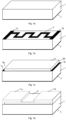
- Figure 1a shows a ceramic substrate 1 in the form of a cuboid according to a first embodiment of the invention.
- the ceramic substrate 1 has a maximum length of 10 mm, a maximum width of 5 mm and a maximum height of 3 mm.
- the ceramic substrate 1 can comprise one or more materials from the group: Al2O3, AlSiC, AIN, B4C, BN, PBN, MgO, SiC, SiSiC, SSiC, Si3N4, YSZ or PZT.
- a sinterable metallization 3 is arranged on one of the first sides, or the top side of the ceramic substrate 1 which is opposite the second side.
- the sinterable metallization 3 can comprise one material or more materials from the group: NiAu, NiPdAu, AgPd, AuPd, Cu, Au or Ag and can be arranged over the entire surface of the second side of the ceramic substrate 1.
- Figure 1b shows this previously in Figure 1a shown ceramic substrate 1 with a resistance element formed as a structured metal layer 5, which is arranged on the first side of the ceramic substrate 1 with a first connection 7a and a second connection 7b.
- the metal layer 5 is, as in Figure 1b shown, designed as a conductor track that runs meander-shaped between its ends, which are formed by the first connection 7a and the second connection 7b, and has a defined resistance value and temperature coefficient at a certain temperature.
- the first connection 7a and the second connection 7b are each designed as a strip-shaped conductor track section is shown.
- the first and the second connection can also simply be formed by the conductor track ends of the meandering conductor track.
- Figure 1c shows the previously Figure 1b shown arrangement with an insulation layer 9 on the metal layer 5 and the first side of the ceramic substrate 1.
- a first region 8a on the first terminal 7a and a second region 8b on the second terminal 7b are uncovered by the insulation layer 9.
- the first region 8a and the second region 8b are opposite each other and the insulation layer 9 is formed by a glass or glass-ceramic material.
- Figure 1d shows the previously Figure 1c shown arrangement with a first contact pad 11a, which electrically contacts the first connection 7a via the first region 8a, and a second contact pad 11b, which electrically contacts the second connection 7b via the second region 8b.
- the material of the respective contact pads 11a, 11b contacts the respective connection 7a, 7b in order to achieve an electrical connection of the contact pads 11a, 11b to the connections 7a, 7b.
- the contact pads 11a, 11b cover a region of the surface of the insulation layer 9 that runs parallel to the first side of the ceramic substrate 1 with the resistance element arranged thereon. In the embodiment shown, the contact pads 11a, 11b also cover a region of the surface of the insulation layer 9 that runs perpendicular to the first side of the ceramic substrate 1.
- FIGS. 2a, 2b, 2c, 2d show further schematic views of a structure of a resistance element according to a second embodiment of the invention.
- the insulation layer is arranged essentially over the entire surface of the first side of the ceramic substrate 1' and a recess 8a', 8b', in the form of an opening, is arranged in the material of the insulation layer 9' in order to enable electrical contacting of the underlying connections 7a', 7b'.
- a first region 8a' on the first terminal 7a' and a second region 8b' on the second terminal 7b' are uncovered by the insulation layer 9'.
- the first region 8a' and the second region 8b' are opposite each other and the insulation layer 9' is formed by a glass or glass-ceramic material.
- connections 7a', 7b' can be contacted via an electrical conductor that extends through the openings and is in electrical contact with the material of the contact pads 11a', 11b'.
- part of the material of the contact pads 11a', 11b' can extend through the openings and be in direct electrical contact with the connections 7a', 7b'.
- the contact pads 11 a ⁇ , 11b' cover a region of the surface of the insulation layer 9' which runs parallel to the first side of the ceramic substrate 1' with the resistance element arranged thereon.
- the resistance layer is formed over the entire surface of the substrate and without structuring.
Landscapes
- Engineering & Computer Science (AREA)
- Microelectronics & Electronic Packaging (AREA)
- Chemical & Material Sciences (AREA)
- Ceramic Engineering (AREA)
- Inorganic Chemistry (AREA)
- Physics & Mathematics (AREA)
- Electromagnetism (AREA)
- Manufacturing & Machinery (AREA)
- Parts Printed On Printed Circuit Boards (AREA)
- Non-Adjustable Resistors (AREA)
- Details Of Resistors (AREA)
- Apparatuses And Processes For Manufacturing Resistors (AREA)
Description
- Die vorliegende Erfindung betrifft ein Widerstandsbauelement zur Oberflächenmontage auf einer Leiterplatte. Weiterhin betrifft die vorliegende Erfindung eine Leiterplatte mit zumindest einem darauf angeordneten Widerstandsbauelement. Die Dokumente
KR20180072489A RU2158419C1 JP2006080322A JP3665385B2 - In Leistungshalbleitermodulen werden elektronische Bauteile, wie beispielsweise Widerstandsbauelemente mittels Oberflächenmontage auf Leiterplatten gesetzt. Hierfür werden oft Widerstandsbauelemente, die keine Drahtanschlüsse besitzen, mittels lötfähiger Anschlussflächen direkt auf die Leiterplatte gelötet.
- Sinterbare Widerstandbauelemente, wie beispielsweise Temperatursensoren oder Widerstände für die Leistungselektronik, können auch auf der Leiterplatte in Oberflächenmontage angeordnet werden. Hierzu werden üblicherweise zylindrische Bauelemente mit einer zum Sintern bestimmten, üblicherweise metallisierten und ebenen Unterseite mittels einer Sinterschicht, beispielsweiser einer silberhaltigen Sinterpaste mit einer Oberfläche der Leiterplatte elektrisch leitend verbunden. Die Kontaktierung kann mittels der metallisierten Unterseite und zumindest einem Kontaktpad, das auf einer der Unterseite gegenüberliegenden Oberseite des Widerstandsbauelements angeordnet ist, erfolgen. Um höhere elektrische Belastungen zu erreichen, kann die Kontaktierung auch durch zwei auf der Oberseite des Widerstandbauelements angeordnete Kontaktpads erfolgen, die elektrisch isoliert gegenüber der metallisierten Unterseite gehalten sind. Die oberseitige Kontaktierung der Kontaktpads erfolgt üblicherweise durch Drahtbonden, Löten, oder Sintern. Die
DE102010050315B4 beschreibt beispielsweise ein elektrisches Bauelement mit Kontaktpads zur Kontaktierung auf der Oberseite des elektrischen Bauelements und einer gegenüberliegenden elektrisch isolierten Metallisierung zum Sintern auf potentialtragenden Flächen, wie beispielsweise auf eine Leiterbahn, die auf der Leiterplatte verläuft. - Die Kontaktflächen der aus dem Stand der Technik bekannten Widerstandsbauelemente zur Oberflächenmontage sind jedoch oft wegen den geringen Abmaßen des Widerstandsbauelements räumlich stark begrenzt ausgestaltet. Deshalb ist eine zuverlässige elektrische Kontaktierung der Kontaktpads nur schwierig zu erreichen.
- Aufgabe der vorliegenden Erfindung ist es daher, ein verbessertes Widerstandsbauelement zur Oberflächenmontage auf einer Leiterplatte bereitzustellen.
- Diese Aufgabe wird erfindungsgemäß durch ein Widerstandsbauelement gemäß des Gegenstands des Anspruchs 1 gelöst.
- Das erfindungsgemäße Widerstandsbauelement zur Oberflächenmontage auf einer Leiterplatte weist hierfür auf:
- ein Keramik-Substrat mit einer ersten Seite und einer gegenüberliegenden zweiten Seite, wobei auf der zweiten Seite eine sinterfähige Metallisierung zumindest bereichsweise angeordnet ist;
- ein Widerstandselement aufweisend eine Metallschicht angeordnet zumindest bereichsweise auf der ersten Seite des Keramik-Substrats mit einem ersten Anschluss und einem zweiten Anschluss;
- eine Isolationsschicht angeordnet zumindest bereichsweise auf dem Widerstandselement und dem Keramik-Substrat, wobei ein erster Bereich auf dem ersten Anschluss und ein zweiter Bereich auf dem zweiten Anschluss unbedeckt von der Isolationsschicht verbleibt; und
- ein erstes Kontaktpad, das den ersten Anschluss über den ersten Bereich elektrisch kontaktiert, und ein zweites Kontaktpad das den zweiten Anschluss über den zweiten Bereich elektrisch kontaktiert, wobei das erste Kontaktpad einen ersten Oberflächenbereich der Isolationsschicht zumindest bereichsweise bedeckt und das zweite Kontaktpad einen zweiten Oberflächenbereich der Isolationsschicht zumindest bereichsweise bedeckt, und das erste und das zweite Kontaktpad voneinander räumlich getrennt auf der Isolationsschicht angeordnet sind.
- Das Keramik-Substrat kann beispielsweise ein oder mehrere Materialien aus der Gruppe: Al2O3, AlSiC, AIN, B4C, BN, PBN, MgO, SiC, SiSiC, SSiC, Si3N4, YSZ oder PZT umfassen und plattenförmig bereitgestellt werden, zum Aufbau einer Vielzahl von Widerstandsbauelementen auf dem Keramik-Substrat. Nach dem Aufbau der Widerstandsbauelemente, kann das Keramik-Substrat strukturiert werden, um die einzelnen Widerstandsbauelemente zu erhalten. Die elektrisch isolierenden Eigenschaften des Keramik-Substrats ermöglichen eine Anordnung der Kontaktpads auf der ersten Seite des Keramik-Substrats, die elektrisch isolierend gegenüber der metallisierten zweiten Seite des Keramik-Substrats gehalten werden.
- Die sinterfähige Metallisierung kann beispielsweise ein oder mehrere Materialien aus der Gruppe: NiAu, NiPdAu, AgPd, AuPd, Au, Ag oder Cu aufweisen und bereichsweise oder vollflächig auf der zweiten Seite des Keramik-Substrats angeordnet sein.
- Das erfindungsgemäße Widerstandselement umfasst eine Metallschicht mit einem ersten Anschluss und einem zweiten Anschluss, bzw. wird mit der Metallschicht hergestellt. Die Metallschicht ist zumindest bereichsweise auf der ersten Seite des Keramik-Substrats angeordnet. Die Metallschicht kann als eine Leiterbahn ausgestaltet sein, die zwischen ihren Enden flächig, mäanderförmig oder wendelförmig verläuft und einen definierten Widerstandswert und Temperaturkoeffizient bei einer bestimmten Temperatur hat.
- Als Isolationsschicht kann eine elektrisch isolierende Schicht, beispielsweise eine Glaskeramik, verstanden werden, die angeordnet ist auf Bereichen der Metallschicht und auf Bereichen der ersten Seite des Keramik-Substrats, die nicht von der Metallschicht bedeckt sind. Ein erster Bereich auf dem ersten Anschluss und ein zweiter Bereich auf dem zweiten Anschluss verbleiben unbedeckt von der Isolationsschicht. Beispielsweise kann die Isolationsschicht eine erste Seite des Keramik-Substrats bis auf den ersten Bereich über dem ersten Anschluss und dem zweiten Bereich über dem zweiten Anschluss vollständig bedecken. Der unbedeckte erste Bereich und zweite Bereich können als Öffnungen ausgestaltet sein, die eine elektrische Kontaktierung des jeweiligen Anschlusses ermöglicht, beispielsweise über einen Abschnitt eines elektrischen Leiters, der sich durch die Öffnungen in der Isolationsschicht erstreckt und eine Kontaktierung der Anschlüsse auf der der ersten Oberfläche des Keramik-Substrats abgewendeten Seite der Isolationsschicht ermöglicht. Die elektrische Kontaktierung der Anschlüsse kann auch durch direkt durch das Material der Kontaktpads hergestellt werden. Unter dem Begriff "Öffnung" kann auch eine Aussparung oder ein von der Isolationsschicht unbedeckter Bereich der unter der Isolationsschicht liegenden ersten Seite des Keramiksubstrats verstanden werden.
- Die Kontaktpads decken jeweils einen Oberflächenbereich der Isolationsschicht ab. Als "Kontaktpad" kann eine dünne Schicht eines elektrisch leitenden Materials verstanden werden, dass im Wesentlichen eben auf der Oberfläche der Isolationsschicht angeordnet ist und mit einem Anschluss der Metallschicht indirekt oder direkt verbunden ist.
- Unter "räumlich getrennt auf der Isolationsschicht angeordnet" kann eine Anordnung des ersten Kontaktpads und des zweiten Kontaktpads auf der Isolationsschicht verstanden werden, so dass sich die beiden Kontaktpads nicht berühren.
- Mit der Erfindung ist es erstmalig gelungen ein Widerstandsbauelement zur Oberflächenmontage auf einer Leiterplatte zur Verfügung zu stellen mit Kontaktpads, die wegen ihrer Anordnung zumindest bereichsweise auf der Isolationsschicht eine ausreichend große Fläche für die Kontaktierung mit Dickdraht, beispielsweise mittels Ballbonding oder Wedgebonding bereitstellen.
- In einem Beispiel bedecken der erste und der zweite Oberflächenbereich zusammen mindestens 70% einer Gesamtoberfläche der Isolationsschicht auf der ersten Seite des Keramik-Substrats.
- Vorteilhaft steht bei dem erfindungsgemäßen Widerstandsbauelement fast der gesamte Oberflächenbereich der Isolationsschicht, die sich wiederum über die zweite Seite des Keramiksubstrats erstrecken kann, zur Verfügung. Somit kann die Oberfläche der Kontaktpads im Vergleich zu den aus dem Stand der Technik bekannten Widerstandsbauelementen erheblich vergrößert werden.
- In einem Beispiel bedecken der erste und der zweite Oberflächenbereich zumindest bereichsweise eine Oberfläche der Isolationsschicht die parallel zu der ersten Seite des Keramik-Substrats mit dem darauf angeordneten Widerstandselement verläuft.
- Vorteilhaft sind die Kontaktpads parallel zu der ersten Seite des Substrats und der Leiterplatte angeordnet. Diese Anordnung ermöglicht eine gute Kontaktierbarkeit mittels der bekannten Bonding-Verfahren.
- In einem weiteren Beispiel bedecken der erste und der zweite Oberflächenbereich zumindest bereichsweise eine Oberfläche der Isolationsschicht die senkrecht zu der ersten Seite des Keramik-Substrats mit dem darauf angeordneten Widerstandselement verläuft.
- Die Anordnung senkrecht zu der ersten Seite des Keramik-Substrats kann alternativ oder zusätzlich zu der Anordnung parallel zu der ersten Seite des Keramik-Substrats erfolgen.
- Vorteilhaft kann durch eine Kombination der parallelen und seitlichen Anordnung der Oberflächenbereiche die Oberfläche der Kontaktpads weiter vergrößert werden.
- In einem Beispiel sind/ist der erste und/oder der zweite Bereich unbedeckt von der Isolationsschicht in Form einer Öffnung in dem Material der Isolationsschicht ausgebildet.
- Vorteilhaft umgibt das Material der Isolationsschicht die Öffnung auf dem wiederum die Kontaktpads angeordnet sein können. In einem Beispiel erstreckt sich das Material der Kontaktpads durch die Öffnungen, um somit die Anschlüsse des Widerstandselements elektrisch zu kontaktieren.
- In einem alternativen Beispiel sind/ist der erste und der zweite Bereich unbedeckt von der Isolationsschicht an zwei gegenüberliegenden Enden des Keramik-Substrats angeordnet und die beiden Anschlüsse sind jeweils an einem der gegenüberliegenden Enden des Keramik-Substrats angeordnet.
- Die Isolationsschicht ist in diesem Beispiel in einem mittleren Bereich auf dem Keramik-Substrat angeordnet und erstreckt sich nur bis zu den Anschlüssen des Widerstandselements. Die Öffnungen sind in diesem Beispiel an den Seiten der Isolationsschicht angeordnet.
- In einem weiteren Beispiel deckt die Isolationsschicht die erste Seite des Keramik-Substrats mit dem darauf angeordneten Widerstandselement vollständig ab und der erste und/oder der zweite Bereich unbedeckt von der Isolationsschicht ist zumindest bereichsweise an dem Keramik-Substrat senkrecht zu der ersten Seite des Keramik-Substrats angeordnet und der erste und/oder der zweite Anschluss ist jeweils an einem von zwei gegenüberliegenden Enden des Keramik-Substrat senkrecht zu der ersten Seite des Keramik-Substrats angeordnet.
- In einem weiteren Beispiel hat das Keramik-Substrat eine maximale Länge von 10 mm, eine maximale Breite von 5 mm und eine maximale Höhe von 3 mm.
- In noch einem Beispiel umfasst die Isolationsschicht ein Glas oder ein Glaskeramik-Material.
- Vorteilhaft kann durch eine Glaskeramik eine Isolationsschicht mit sehr guten Isolationseigenschaften geschaffen werden, die wegen der guten Isolationseigenschaften sehr dünn ausgestaltet sein kann.
- In einem weiteren Beispiel ist der erste und der zweiten Oberflächenbereich angepasst zum Wedgebonding von Aluminiumdickdraht, insbesondere von Aluminiumdickdraht mit einem Durchmesser von größer oder gleich 25 µm.
- In noch einem Beispiel umfasst die sinterfähige Metallisierung eine Silber-Palladium Metallisierung, und/oder das Keramik-Substrat umfasst eine Al2O3-Keramik.
- In einem weiteren Beispiel umfasst die Metallschicht eine Strukturierung, ein PT100 oder PT1000 Widerstandselement, insbesondere ein Pt- Dünnschicht oder Dickschicht Widerstandselement mit Trimmstrecke, und ist angepasst zum Messen einer Temperatur, und wobei die Strukturierung der Metallschicht sich mäanderförmig zwischen dem ersten Anschluss und dem zweiten Anschluss erstreckt.
- In noch einem Beispiel umfasst die Metallschicht ein Material mit einem Temperaturkoeffizienten von kleiner 500 ppm K-1 bei Raumtemperatur, insbesondere Metalllegierungen enthaltend Chrom, Nickel, Eisen, Zink, Silber oder Palladium.
- Die Erfindung schlägt auch eine Leiterplatte mit zumindest einem darauf angeordneten erfindungsgemäßen Widerstandsbauelement vor.
- Weitere Merkmale und Vorteile der Erfindung ergeben sich aus der nachfolgenden Beschreibung, in der bevorzugte Ausführungsformen der Erfindung anhand von schematischen Zeichnungen erläutert sind.
- Dabei zeigen:
- Figuren 1a, 1b, 1c, 1d
- schematische Ansichten eines Aufbaus eines Widerstandselements gemäß einer ersten Ausführungsform der Erfindung; und
- Figuren 2a, 2b, 2c, 2d
- schematische Ansichten eines Aufbaus eines Widerstandselements gemäß einer zweiten Ausführungsform der Erfindung.
-
Figur 1a zeigt ein Keramik-Substrat 1 in Form eines Quaders gemäß einer ersten Ausführungsform der Erfindung. In der gezeigten Ausführungsform hat das Keramik-Substrat 1 eine maximale Länge von 10 mm, eine maximale Breite von 5 mm und eine maximale Höhe von 3 mm. In der gezeigten Ausführungsform kann das Keramik-Substrat 1 ein oder mehrere Materialien aus der Gruppe: Al2O3, AlSiC, AIN, B4C, BN, PBN, MgO, SiC, SiSiC, SSiC, Si3N4, YSZ oder PZT umfassen. Auf einer der ersten Seite, oder der Oberseite des Keramik-Substrats 1 die der zweiten Seite gegenüberliegt, ist eine sinterfähige Metallisierung 3 angeordnet. Die sinterfähige Metallisierung 3 kann in der gezeigten Ausführungsform ein Material oder mehrere Materialien aus der Gruppe: NiAu, NiPdAu, AgPd, AuPd, Cu, Au oder Ag aufweisen und kann vollflächig auf der zweiten Seite des Keramik-Substrats 1 angeordnet sein. -
Figur 1b zeigt das zuvor inFigur 1a gezeigte Keramik-Substrat 1 mit einem Widerstandselement ausgebildet als eine strukturierte Metallschicht 5, die auf der ersten Seite des Keramik-Substrats 1 mit einem ersten Anschluss 7a und einem zweiten Anschluss 7b angeordnet ist. - Die Metallschicht 5 ist, wie in
Figur 1b gezeigt, als eine Leiterbahn ausgestaltet, die zwischen ihren Enden, die durch den ersten Anschluss 7a und den zweiten Anschluss 7b gebildet werden, mäanderförmig verläuft und einen definierten Widerstandswert und Temperaturkoeffizienten bei einer bestimmten Temperatur hat. In der gezeigten Ausführungsform sind der erste Anschluss 7a und der zweite Anschluss 7b jeweils als ein streifenförmiger Leiterbahnabschnitt gezeigt. In weiteren Ausführungsformen kann der erste und der zweite Anschluss auch einfach durch die Leiterbahnenden der mäanderförmig angeordneten Leiterbahn gebildet werden. -
Figur 1c zeigt die zuvor inFigur 1b gezeigte Anordnung mit einer Isolationsschicht 9 auf der Metallschicht 5 und der ersten Seite des Keramik-Substrats 1. Wie es in derFigur 1c gezeigt wird, ist ein erster Bereich 8a auf dem ersten Anschluss 7a und ein zweiter Bereich 8b auf dem zweiten Anschluss 7b unbedeckt von der Isolationsschicht 9. In der gezeigten Ausführungsform liegen sich der erste Bereich 8a und der zweite Bereich 8b gegenüber und der die Isolationsschicht 9 wird durch ein Glas oder Glaskeramik-Material gebildet. -
Figur 1d zeigt die zuvor inFigur 1c gezeigte Anordnung mit einem ersten Kontaktpad 11a, das den ersten Anschluss 7a über den ersten Bereich 8a elektrisch kontaktiert, und ein zweites Kontaktpad 11b das den zweiten Anschluss 7b über den zweiten Bereich 8b elektrisch kontaktiert. Das Material der jeweiligen Kontaktpads 11a, 11b kontaktiert den jeweiligen Anschluss 7a, 7b, um eine elektrische Anbindung der Kontaktpads 11a, 11b an die Anschlüsse 7a, 7b zu erzielen. - Wie es in der
Figur 1d gezeigt ist, bedecken die Kontaktpads 11a, 11b einen Bereich der Oberfläche der Isolationsschicht 9 der parallel zu der ersten Seite des Keramik-Substrats 1 mit dem darauf angeordneten Widerstandselement verläuft. In der gezeigten Ausführungsform bedecken die Kontaktpads 11a, 11b auch einen Bereich der Oberfläche der Isolationsschicht 9 der senkrecht zu der ersten Seite des Keramik-Substrats 1 verläuft. - Die
Figuren 2a, 2b, 2c, 2d zeigen weitere schematische Ansichten eines Aufbaus eines Widerstandselements gemäß einer zweiten Ausführungsform der Erfindung. - Die
Figuren 2a und 2b entsprechen den bereits zuvor gezeigtenFiguren 1a und 1b . - In der
Figur 2c ist die Isolationsschicht im Wesentlichen vollflächig auf der ersten Seite des Keramik-Substrats 1' angeordnet und jeweils eine Ausnehmung 8a', 8b', in Form einer Öffnung, ist in dem Material der Isolationsschicht 9' angeordnet, um eine elektrische Kontaktierung der darunterliegenden Anschlüsse 7a', 7b' zu ermöglichen. - Wie es in der
Figur 1c gezeigt wird, ist ein erster Bereich 8a' auf dem ersten Anschluss 7a' und ein zweiter Bereich 8b' auf dem zweiten Anschluss 7b' unbedeckt von der Isolationsschicht 9'. In der gezeigten Ausführungsform liegen sich der erste Bereich 8a' und der zweite Bereich 8b' gegenüber und die Isolationsschicht 9' wird durch ein Glas oder Glaskeramik-Material gebildet. - Die Anschlüsse 7a', 7b' können über einen elektrischen Leiter kontaktiert werden, der sich durch die Öffnungen erstreckt und mit dem Material der Kontaktpads 11 a', 11b' elektrisch in Kontakt steht. Alternativ kann sich auch ein Teil des Materials der Kontaktpads 11a', 11b' durch die Öffnungen erstrecken und mit den Anschlüsse 7a', 7b' direkt in elektrischem Kontakt stehen.
- Wie es in der
Figur 2d gezeigt wird, bedecken die Kontaktpads 11 a`, 11b' einen Bereich der Oberfläche der Isolationsschicht 9' der parallel zu der ersten Seite des Keramik-Substrats 1' mit dem darauf angeordneten Widerstandselement verläuft. - In einer weiteren (nicht gezeigten) Ausführungsform ist die Widerstandsschicht vollflächig und ohne Strukturierung auf dem Substrat ausgebildet.
-
- 1, 1'
- Keramik-Substrat
- 3, 3'
- sinterfähige Metallisierung
- 5, 5'
- Metallschicht
- 7a, 7a'
- erster Anschluss
- 7b, 7b'
- zweiter Anschluss
- 8a, 8a'
- erster Bereich
- 8b, 8b'
- zweiter Bereich
- 9, 9'
- Isolationsschicht
- 11a, 11a'
- erstes Kontaktpad
- 11b, 11b'
- zweites Kontaktpad
Claims (14)
- Widerstandsbauelement zur Oberflächenmontage auf einer Leiterplatte, aufweisend:ein Keramik-Substrat (1, 1 ') mit einer ersten Seite und einer gegenüberliegenden zweiten Seite, wobei auf der zweiten Seite eine sinterfähige Metallisierung (3, 3') zumindest bereichsweise angeordnet ist;ein Widerstandselement aufweisend eine Metallschicht (5, 5') angeordnet zumindest bereichsweise auf der ersten Seite des Keramik-Substrats (1, 1') mit einem ersten Anschluss (7a, 7a') und einem zweiten Anschluss (7b, 7b');eine Isolationsschicht (9, 9') angeordnet zumindest bereichsweise auf dem Widerstandselement und dem Keramik-Substrat (1, 1'), wobei ein erster Bereich (8a, 8a') auf dem ersten Anschluss (7a, 7a') und ein zweiter Bereich (8b, 8b') auf dem zweiten Anschluss (7b, 7b') unbedeckt von der Isolationsschicht (9, 9') verbleibt; undein erstes Kontaktpad (11a, 11a'), das den ersten Anschluss (7a, 7a') über den ersten Bereich (8a, 8a') elektrisch kontaktiert, und ein zweites Kontaktpad (11b, 11b') das den zweiten Anschluss (7b, 7b') über den zweiten Bereich (8b, 8b') elektrisch kontaktiert;dadurch gekennzeichnet, dassdas erste Kontaktpad (11a, 11 a') einen ersten Oberflächenbereich der Isolationsschicht (9, 9') zumindest bereichsweise bedeckt und das zweite Kontaktpad (11b, 11b') einen zweiten Oberflächenbereich der Isolationsschicht (9, 9') zumindest bereichsweise bedeckt, und das erste (11a, 11a') und das zweite (11b, 11b') Kontaktpad voneinander räumlich getrennt auf der Isolationsschicht (9, 9') angeordnet sind.
- Widerstandsbauelement nach Anspruch 1, dadurch gekennzeichnet, dass der erste und der zweite Oberflächenbereich zusammen mindestens 70% einer Gesamtoberfläche der Isolationsschicht (9, 9') auf der ersten Seite des Keramik-Substrats (1, 1') bedecken.
- Widerstandsbauelement nach Anspruch 1 oder 2, dadurch gekennzeichnet, dass der erste und der zweite Oberflächenbereich zumindest bereichsweise eine Oberfläche der Isolationsschicht (9, 9') bedecken die parallel zu der ersten Seite des Keramik-Substrats mit dem darauf angeordneten Widerstandselement verläuft.
- Widerstandsbauelement nach einem der vorangehenden Ansprüche, dadurch
gekennzeichnet, dass
der erste und der zweite Oberflächenbereich zumindest bereichsweise eine Oberfläche der Isolationsschicht (9) bedecken die senkrecht zu der ersten Seite des Keramik-Substrats (1) mit dem darauf angeordneten Widerstandselement verläuft. - Widerstandsbauelement nach einem der vorangehenden Ansprüche, dadurch
gekennzeichnet, dass
der erste (8a') und/oder der zweite (8b') Bereich unbedeckt von der Isolationsschicht (9') in Form einer Öffnung in dem Material der Isolationsschicht (9') ausgebildet ist. - Widerstandsbauelement nach einem der Ansprüche 1 bis 4, dadurch gekennzeichnet, dass
der erste (8a) und der zweite Bereich (8b) unbedeckt von der Isolationsschicht (9) an zwei gegenüberliegenden Enden des Keramik-Substrats (1) angeordnet sind und der erste (7a) und der zweite (7b) Anschluss jeweils an einem der zwei gegenüberliegenden Enden angeordnet ist. - Widerstandsbauelement nach einem der Ansprüche 1 bis 4, dadurch gekennzeichnet, dass
die Isolationsschicht (9') die erste Seite des Keramik-Substrats (1') mit dem darauf angeordneten Widerstandselement vollständig abdeckt und der erste (8a') und/oder der zweite Bereich (8b') unbedeckt von der Isolationsschicht (9') zumindest bereichsweise an dem Keramik-Substrat (1') senkrecht zu der ersten Seite des Keramik-Substrats (1') angeordnet ist und der erste und/oder der zweite Anschluss jeweils an einem von zwei gegenüberliegenden Enden des Keramik-Substrat senkrecht zu der ersten Seite des Keramik-Substrats (1, 1') angeordnet ist. - Widerstandsbauelement nach einem der vorangehenden Ansprüche, dadurch
gekennzeichnet, dass
das Keramik-Substrat (1, 1') eine maximale Länge von 10 mm, eine maximale Breite von 5 mm und eine maximale Höhe von 3 mm hat. - Widerstandsbauelement nach einem der vorangehenden Ansprüche, dadurch
gekennzeichnet, dass
die Isolationsschicht (9, 9') ein Glas oder ein Glaskeramik-Material umfasst. - Widerstandsbauelement nach einem der vorangehenden Ansprüche, dadurch
gekennzeichnet, dass
der erste und der zweiten Oberflächenbereich angepasst sind zum Wedgebonding von Aluminiumdickdraht, insbesondere von Aluminiumdickdraht mit einem Durchmesser von größer oder gleich 25 µm. - Widerstandsbauelement nach einem der vorangehenden Ansprüche, dadurch
gekennzeichnet, dass
die sinterfähige Metallisierung (3, 3') eine Silber-Palladium Metallisierung umfasst, und/oder das Keramik-Substrat (1, 1 ') eine Al2O3-Keramik umfasst. - Widerstandsbauelement nach einem der vorangehenden Ansprüche, dadurch gekennzeichnet, dass
die Metallschicht (5, 5') eine Strukturierung umfasst, ein PT100 oder PT1000 Widerstandselement umfasst, insbesondere ein Pt- Dünnschicht oder Dickschicht Widerstandselement mit Trimmstrecke, und angepasst zum Messen einer Temperatur, und wobei die Strukturierung der Metallschicht (5, 5') sich mäanderförmig zwischen dem ersten Anschluss (7a, 7a') und dem zweiten (7b, 7b') Anschluss erstreckt. - Widerstandsbauelement nach einem der Ansprüche 1 bis 11, dadurch gekennzeichnet,
dass
die Metallschicht (5, 5') ein Material mit einem Temperaturkoeffizienten von kleiner 500 ppm K-1 bei Raumtemperatur umfasst, insbesondere Metalllegierungen enthaltend Chrom, Nickel, Eisen, Zink, Silber oder Palladium. - Leiterplatte mit zumindest einem darauf angeordneten Widerstandsbauelement nach einem der vorangehenden Ansprüche.
Applications Claiming Priority (2)
| Application Number | Priority Date | Filing Date | Title |
|---|---|---|---|
| DE202018004354.0U DE202018004354U1 (de) | 2018-09-19 | 2018-09-19 | Widerstandsbauelement zur Oberflächenmontage auf einer Leiterplatte und Leiterplatte mit zumindest einem darauf angeordneten Widerstandsbauelement |
| PCT/EP2019/071193 WO2020057850A1 (de) | 2018-09-19 | 2019-08-07 | Widerstandsbauelement zur oberflächenmontage auf einer leiterplatte und leiterplatte mit zumindest einem darauf angeordneten widerstandsbauelement |
Publications (2)
| Publication Number | Publication Date |
|---|---|
| EP3853873A1 EP3853873A1 (de) | 2021-07-28 |
| EP3853873B1 true EP3853873B1 (de) | 2024-12-04 |
Family
ID=64278526
Family Applications (1)
| Application Number | Title | Priority Date | Filing Date |
|---|---|---|---|
| EP19752476.2A Active EP3853873B1 (de) | 2018-09-19 | 2019-08-07 | Widerstandsbauelement zur oberflächenmontage auf einer leiterplatte und leiterplatte mit zumindest einem darauf angeordneten widerstandsbauelement |
Country Status (7)
| Country | Link |
|---|---|
| US (1) | US11547000B2 (de) |
| EP (1) | EP3853873B1 (de) |
| JP (1) | JP7288043B2 (de) |
| KR (1) | KR102552987B1 (de) |
| CN (2) | CN117438165A (de) |
| DE (1) | DE202018004354U1 (de) |
| WO (1) | WO2020057850A1 (de) |
Families Citing this family (3)
| Publication number | Priority date | Publication date | Assignee | Title |
|---|---|---|---|---|
| EP3961170A1 (de) * | 2020-08-27 | 2022-03-02 | Heraeus Nexensos GmbH | Temperatursensor und verfahren zur herstellung eines derartigen temperatursensors |
| JP7531976B2 (ja) | 2021-04-09 | 2024-08-13 | エルジー エナジー ソリューション リミテッド | 全固体電池の製造方法及びこれによる全固体電池 |
| CN115966557A (zh) * | 2023-01-17 | 2023-04-14 | 常州承芯半导体有限公司 | 薄膜电阻结构及其形成方法、半导体结构及其形成方法 |
Citations (5)
| Publication number | Priority date | Publication date | Assignee | Title |
|---|---|---|---|---|
| EP0484756A2 (de) * | 1990-11-05 | 1992-05-13 | Isabellenhütte Heusler GmbH KG | Widerstandsanordnung in SMD-Bauweise |
| RU2158419C1 (ru) * | 1999-11-04 | 2000-10-27 | Научно-производственное объединение измерительной техники | Датчик температуры |
| JP3665385B2 (ja) * | 1995-05-15 | 2005-06-29 | ローム株式会社 | 電子部品 |
| JP2006080322A (ja) * | 2004-09-10 | 2006-03-23 | Ishizuka Electronics Corp | チップ型複合電子部品 |
| KR20180072489A (ko) * | 2016-12-21 | 2018-06-29 | 내셔널 청쿵 유니버시티 | 알루미늄 말단 전극을 사용한 칩 저항기의 제조 방법 |
Family Cites Families (24)
| Publication number | Priority date | Publication date | Assignee | Title |
|---|---|---|---|---|
| FR2653588B1 (fr) * | 1989-10-20 | 1992-02-07 | Electro Resistance | Resistance electrique sous forme de puce a montage de surface et son procede de fabrication. |
| DE4025715C1 (de) * | 1990-08-14 | 1992-04-02 | Robert Bosch Gmbh, 7000 Stuttgart, De | |
| US5294910A (en) * | 1991-07-01 | 1994-03-15 | Murata Manufacturing Co., Ltd. | Platinum temperature sensor |
| JP3983392B2 (ja) * | 1998-10-15 | 2007-09-26 | 太陽社電気株式会社 | チップ型部品 |
| TW531867B (en) * | 2000-10-13 | 2003-05-11 | Texas Instruments Inc | Circuit structure integrating the power distribution functions of circuits and leadframes into the chip surface |
| DE10358282A1 (de) * | 2003-12-12 | 2005-07-28 | Georg Bernitz | Bauelement und Verfahren zu dessen Herstellung |
| US7190252B2 (en) * | 2005-02-25 | 2007-03-13 | Vishay Dale Electronics, Inc. | Surface mount electrical resistor with thermally conductive, electrically insulative filler and method for using same |
| DE102005030555A1 (de) * | 2005-06-22 | 2007-01-04 | E.G.O. Elektro-Gerätebau GmbH | Sensoreinrichtung für eine Heizeinrichtung |
| JP2010182891A (ja) * | 2009-02-05 | 2010-08-19 | Hokuriku Electric Ind Co Ltd | 多層回路基板 |
| CN101951726A (zh) * | 2010-09-17 | 2011-01-19 | 昆山华扬电子有限公司 | 内埋电阻的印制线路板及其制作工艺 |
| DE102010050315C5 (de) | 2010-11-05 | 2014-12-04 | Danfoss Silicon Power Gmbh | Verfahren zur Herstellung von gesinterten, elektrischen Baugruppen und damit hergestellte Leistungshalbleitermodule |
| JP5668837B2 (ja) * | 2011-02-24 | 2015-02-12 | 株式会社村田製作所 | 電子部品の実装構造 |
| KR101892750B1 (ko) * | 2011-12-19 | 2018-08-29 | 삼성전기주식회사 | 칩 저항 부품 및 그의 제조 방법 |
| JP6285096B2 (ja) | 2011-12-26 | 2018-02-28 | ローム株式会社 | チップ抵抗器、および、電子デバイス |
| US9633768B2 (en) * | 2013-06-13 | 2017-04-25 | Rohm Co., Ltd. | Chip resistor and mounting structure thereof |
| JP2016152301A (ja) * | 2015-02-17 | 2016-08-22 | ローム株式会社 | チップ抵抗器およびその製造方法 |
| JP2016192509A (ja) * | 2015-03-31 | 2016-11-10 | Koa株式会社 | チップ抵抗器 |
| JP2017069441A (ja) * | 2015-09-30 | 2017-04-06 | Koa株式会社 | チップ抵抗器 |
| JP6572143B2 (ja) | 2016-01-27 | 2019-09-04 | Koa株式会社 | チップ抵抗器およびその製造方法 |
| JP6706942B2 (ja) * | 2016-03-24 | 2020-06-10 | Koa株式会社 | 部品内蔵型回路基板 |
| JP6792374B2 (ja) * | 2016-08-08 | 2020-11-25 | ローム株式会社 | チップ部品およびその製造方法、ならびに、チップ部品を備えた回路モジュール |
| KR102527724B1 (ko) | 2016-11-15 | 2023-05-02 | 삼성전기주식회사 | 칩 저항 소자 및 칩 저항 소자 어셈블리 |
| US10438729B2 (en) * | 2017-11-10 | 2019-10-08 | Vishay Dale Electronics, Llc | Resistor with upper surface heat dissipation |
| US11011290B2 (en) * | 2017-12-12 | 2021-05-18 | Koa Corporation | Method for manufacturing resistor, and resistor |
-
2018
- 2018-09-19 DE DE202018004354.0U patent/DE202018004354U1/de active Active
-
2019
- 2019-08-07 WO PCT/EP2019/071193 patent/WO2020057850A1/de not_active Ceased
- 2019-08-07 CN CN202311349138.8A patent/CN117438165A/zh active Pending
- 2019-08-07 CN CN201980053761.4A patent/CN112567483A/zh active Pending
- 2019-08-07 JP JP2021510451A patent/JP7288043B2/ja active Active
- 2019-08-07 US US17/277,577 patent/US11547000B2/en active Active
- 2019-08-07 KR KR1020217010807A patent/KR102552987B1/ko active Active
- 2019-08-07 EP EP19752476.2A patent/EP3853873B1/de active Active
Patent Citations (5)
| Publication number | Priority date | Publication date | Assignee | Title |
|---|---|---|---|---|
| EP0484756A2 (de) * | 1990-11-05 | 1992-05-13 | Isabellenhütte Heusler GmbH KG | Widerstandsanordnung in SMD-Bauweise |
| JP3665385B2 (ja) * | 1995-05-15 | 2005-06-29 | ローム株式会社 | 電子部品 |
| RU2158419C1 (ru) * | 1999-11-04 | 2000-10-27 | Научно-производственное объединение измерительной техники | Датчик температуры |
| JP2006080322A (ja) * | 2004-09-10 | 2006-03-23 | Ishizuka Electronics Corp | チップ型複合電子部品 |
| KR20180072489A (ko) * | 2016-12-21 | 2018-06-29 | 내셔널 청쿵 유니버시티 | 알루미늄 말단 전극을 사용한 칩 저항기의 제조 방법 |
Also Published As
| Publication number | Publication date |
|---|---|
| WO2020057850A1 (de) | 2020-03-26 |
| KR20210046816A (ko) | 2021-04-28 |
| CN112567483A (zh) | 2021-03-26 |
| DE202018004354U1 (de) | 2018-10-15 |
| KR102552987B1 (ko) | 2023-07-06 |
| CN117438165A (zh) | 2024-01-23 |
| EP3853873A1 (de) | 2021-07-28 |
| US11547000B2 (en) | 2023-01-03 |
| JP7288043B2 (ja) | 2023-06-06 |
| JP2021535607A (ja) | 2021-12-16 |
| US20210307178A1 (en) | 2021-09-30 |
Similar Documents
| Publication | Publication Date | Title |
|---|---|---|
| DE102010050315C5 (de) | Verfahren zur Herstellung von gesinterten, elektrischen Baugruppen und damit hergestellte Leistungshalbleitermodule | |
| DE102013213448B4 (de) | Elektronikbaugruppe mit Leistungshalbleiter | |
| EP0972288B1 (de) | Verfahren zur herstellung einer sensoranordnung für die temperaturmessung | |
| EP3853873B1 (de) | Widerstandsbauelement zur oberflächenmontage auf einer leiterplatte und leiterplatte mit zumindest einem darauf angeordneten widerstandsbauelement | |
| EP4498053B1 (de) | Sensorelement und verfahren zur herstellung eines sensorelements | |
| EP3371562B1 (de) | Sensorelement und verfahren zur herstellung eines sensorelements | |
| EP1756537B1 (de) | Temperaturfühler und verfahren zu dessen herstellung | |
| EP3615903A1 (de) | Sensor zur erfassung eines räumlichen temperaturprofils und verfahren zur herstellung einer sensoreinheit | |
| DE112020001997T5 (de) | Stromerfassungswiderstand | |
| EP0809094A1 (de) | Verfahren zur Herstellung einer Sensoranordung für die Temperaturmessung | |
| EP2875514B1 (de) | Elektrisches bauelement umfassend ein anschlusselement mit einem kunststoffkörper | |
| EP1286144B1 (de) | Verfahren zur Herstellung einer Hybriden Hochtemperaturerfassungseinrichtung | |
| WO2016113080A1 (de) | Kontaktanordnung und leistungsmodul | |
| DE19633486C1 (de) | Verfahren zur Herstellung einer Leiterplatte mit dünnen Leiterbahnen und Anschluß-Kontaktierungsbereichen sowie deren Verwendung | |
| EP3054480B1 (de) | Kontaktanordnung und leistungsmodul | |
| EP3765827B1 (de) | Temperatursensorelement | |
| EP0665560B1 (de) | Hybridschaltungsanordnung | |
| DE102020133985A1 (de) | Sensoranordnung und Verfahren zur Herstellung einer Sensoranordnung | |
| DE102024208362A1 (de) | Leistungshalbleiter-Chip und Leistungsmodul | |
| DE102011103828B4 (de) | Massenproduktion kleiner Temepratursensoren mit Flip-Chips | |
| DE10021367A1 (de) | Detektor für Computertomographen | |
| DE102024122526A1 (de) | Sensoranordnung und Verfahren zur Herstellung einer Sensoranordnung | |
| DE102022204223A1 (de) | Vorrichtung zur Temperaturmessung einer thermischen Quelle und Temperatursensor |
Legal Events
| Date | Code | Title | Description |
|---|---|---|---|
| STAA | Information on the status of an ep patent application or granted ep patent |
Free format text: STATUS: UNKNOWN |
|
| STAA | Information on the status of an ep patent application or granted ep patent |
Free format text: STATUS: THE INTERNATIONAL PUBLICATION HAS BEEN MADE |
|
| PUAI | Public reference made under article 153(3) epc to a published international application that has entered the european phase |
Free format text: ORIGINAL CODE: 0009012 |
|
| STAA | Information on the status of an ep patent application or granted ep patent |
Free format text: STATUS: REQUEST FOR EXAMINATION WAS MADE |
|
| 17P | Request for examination filed |
Effective date: 20210204 |
|
| AK | Designated contracting states |
Kind code of ref document: A1 Designated state(s): AL AT BE BG CH CY CZ DE DK EE ES FI FR GB GR HR HU IE IS IT LI LT LU LV MC MK MT NL NO PL PT RO RS SE SI SK SM TR |
|
| DAV | Request for validation of the european patent (deleted) | ||
| DAX | Request for extension of the european patent (deleted) | ||
| RAP3 | Party data changed (applicant data changed or rights of an application transferred) |
Owner name: HERAEUS NEXENSOS GMBH |
|
| RAP3 | Party data changed (applicant data changed or rights of an application transferred) |
Owner name: YAGEO NEXENSOS GMBH |
|
| GRAP | Despatch of communication of intention to grant a patent |
Free format text: ORIGINAL CODE: EPIDOSNIGR1 |
|
| STAA | Information on the status of an ep patent application or granted ep patent |
Free format text: STATUS: GRANT OF PATENT IS INTENDED |
|
| INTG | Intention to grant announced |
Effective date: 20240702 |
|
| GRAS | Grant fee paid |
Free format text: ORIGINAL CODE: EPIDOSNIGR3 |
|
| GRAA | (expected) grant |
Free format text: ORIGINAL CODE: 0009210 |
|
| STAA | Information on the status of an ep patent application or granted ep patent |
Free format text: STATUS: THE PATENT HAS BEEN GRANTED |
|
| AK | Designated contracting states |
Kind code of ref document: B1 Designated state(s): AL AT BE BG CH CY CZ DE DK EE ES FI FR GB GR HR HU IE IS IT LI LT LU LV MC MK MT NL NO PL PT RO RS SE SI SK SM TR |
|
| REG | Reference to a national code |
Ref country code: CH Ref legal event code: EP |
|
| REG | Reference to a national code |
Ref country code: DE Ref legal event code: R096 Ref document number: 502019012603 Country of ref document: DE |
|
| REG | Reference to a national code |
Ref country code: IE Ref legal event code: FG4D Free format text: LANGUAGE OF EP DOCUMENT: GERMAN |
|
| P01 | Opt-out of the competence of the unified patent court (upc) registered |
Free format text: CASE NUMBER: APP_63863/2024 Effective date: 20241202 |
|
| REG | Reference to a national code |
Ref country code: LT Ref legal event code: MG9D |
|
| REG | Reference to a national code |
Ref country code: NL Ref legal event code: MP Effective date: 20241204 |
|
| PG25 | Lapsed in a contracting state [announced via postgrant information from national office to epo] |
Ref country code: HR Free format text: LAPSE BECAUSE OF FAILURE TO SUBMIT A TRANSLATION OF THE DESCRIPTION OR TO PAY THE FEE WITHIN THE PRESCRIBED TIME-LIMIT Effective date: 20241204 |
|
| PG25 | Lapsed in a contracting state [announced via postgrant information from national office to epo] |
Ref country code: FI Free format text: LAPSE BECAUSE OF FAILURE TO SUBMIT A TRANSLATION OF THE DESCRIPTION OR TO PAY THE FEE WITHIN THE PRESCRIBED TIME-LIMIT Effective date: 20241204 |
|
| PG25 | Lapsed in a contracting state [announced via postgrant information from national office to epo] |
Ref country code: BG Free format text: LAPSE BECAUSE OF FAILURE TO SUBMIT A TRANSLATION OF THE DESCRIPTION OR TO PAY THE FEE WITHIN THE PRESCRIBED TIME-LIMIT Effective date: 20241204 |
|
| PG25 | Lapsed in a contracting state [announced via postgrant information from national office to epo] |
Ref country code: ES Free format text: LAPSE BECAUSE OF FAILURE TO SUBMIT A TRANSLATION OF THE DESCRIPTION OR TO PAY THE FEE WITHIN THE PRESCRIBED TIME-LIMIT Effective date: 20241204 |
|
| PG25 | Lapsed in a contracting state [announced via postgrant information from national office to epo] |
Ref country code: NO Free format text: LAPSE BECAUSE OF FAILURE TO SUBMIT A TRANSLATION OF THE DESCRIPTION OR TO PAY THE FEE WITHIN THE PRESCRIBED TIME-LIMIT Effective date: 20250304 |
|
| PG25 | Lapsed in a contracting state [announced via postgrant information from national office to epo] |
Ref country code: GR Free format text: LAPSE BECAUSE OF FAILURE TO SUBMIT A TRANSLATION OF THE DESCRIPTION OR TO PAY THE FEE WITHIN THE PRESCRIBED TIME-LIMIT Effective date: 20250305 Ref country code: LV Free format text: LAPSE BECAUSE OF FAILURE TO SUBMIT A TRANSLATION OF THE DESCRIPTION OR TO PAY THE FEE WITHIN THE PRESCRIBED TIME-LIMIT Effective date: 20241204 |
|
| PG25 | Lapsed in a contracting state [announced via postgrant information from national office to epo] |
Ref country code: RS Free format text: LAPSE BECAUSE OF FAILURE TO SUBMIT A TRANSLATION OF THE DESCRIPTION OR TO PAY THE FEE WITHIN THE PRESCRIBED TIME-LIMIT Effective date: 20250304 |
|
| PG25 | Lapsed in a contracting state [announced via postgrant information from national office to epo] |
Ref country code: NL Free format text: LAPSE BECAUSE OF FAILURE TO SUBMIT A TRANSLATION OF THE DESCRIPTION OR TO PAY THE FEE WITHIN THE PRESCRIBED TIME-LIMIT Effective date: 20241204 |
|
| PG25 | Lapsed in a contracting state [announced via postgrant information from national office to epo] |
Ref country code: SM Free format text: LAPSE BECAUSE OF FAILURE TO SUBMIT A TRANSLATION OF THE DESCRIPTION OR TO PAY THE FEE WITHIN THE PRESCRIBED TIME-LIMIT Effective date: 20241204 |
|
| PG25 | Lapsed in a contracting state [announced via postgrant information from national office to epo] |
Ref country code: PL Free format text: LAPSE BECAUSE OF FAILURE TO SUBMIT A TRANSLATION OF THE DESCRIPTION OR TO PAY THE FEE WITHIN THE PRESCRIBED TIME-LIMIT Effective date: 20241204 |
|
| PG25 | Lapsed in a contracting state [announced via postgrant information from national office to epo] |
Ref country code: IS Free format text: LAPSE BECAUSE OF FAILURE TO SUBMIT A TRANSLATION OF THE DESCRIPTION OR TO PAY THE FEE WITHIN THE PRESCRIBED TIME-LIMIT Effective date: 20250404 |
|
| PG25 | Lapsed in a contracting state [announced via postgrant information from national office to epo] |
Ref country code: PT Free format text: LAPSE BECAUSE OF FAILURE TO SUBMIT A TRANSLATION OF THE DESCRIPTION OR TO PAY THE FEE WITHIN THE PRESCRIBED TIME-LIMIT Effective date: 20250404 |
|
| PG25 | Lapsed in a contracting state [announced via postgrant information from national office to epo] |
Ref country code: EE Free format text: LAPSE BECAUSE OF FAILURE TO SUBMIT A TRANSLATION OF THE DESCRIPTION OR TO PAY THE FEE WITHIN THE PRESCRIBED TIME-LIMIT Effective date: 20241204 |
|
| PGFP | Annual fee paid to national office [announced via postgrant information from national office to epo] |
Ref country code: FR Payment date: 20250610 Year of fee payment: 7 |
|
| PG25 | Lapsed in a contracting state [announced via postgrant information from national office to epo] |
Ref country code: RO Free format text: LAPSE BECAUSE OF FAILURE TO SUBMIT A TRANSLATION OF THE DESCRIPTION OR TO PAY THE FEE WITHIN THE PRESCRIBED TIME-LIMIT Effective date: 20241204 |
|
| PG25 | Lapsed in a contracting state [announced via postgrant information from national office to epo] |
Ref country code: SK Free format text: LAPSE BECAUSE OF FAILURE TO SUBMIT A TRANSLATION OF THE DESCRIPTION OR TO PAY THE FEE WITHIN THE PRESCRIBED TIME-LIMIT Effective date: 20241204 |
|
| PG25 | Lapsed in a contracting state [announced via postgrant information from national office to epo] |
Ref country code: CZ Free format text: LAPSE BECAUSE OF FAILURE TO SUBMIT A TRANSLATION OF THE DESCRIPTION OR TO PAY THE FEE WITHIN THE PRESCRIBED TIME-LIMIT Effective date: 20241204 |
|
| REG | Reference to a national code |
Ref country code: DE Ref legal event code: R097 Ref document number: 502019012603 Country of ref document: DE |
|
| PG25 | Lapsed in a contracting state [announced via postgrant information from national office to epo] |
Ref country code: SE Free format text: LAPSE BECAUSE OF FAILURE TO SUBMIT A TRANSLATION OF THE DESCRIPTION OR TO PAY THE FEE WITHIN THE PRESCRIBED TIME-LIMIT Effective date: 20241204 |
|
| PG25 | Lapsed in a contracting state [announced via postgrant information from national office to epo] |
Ref country code: DK Free format text: LAPSE BECAUSE OF FAILURE TO SUBMIT A TRANSLATION OF THE DESCRIPTION OR TO PAY THE FEE WITHIN THE PRESCRIBED TIME-LIMIT Effective date: 20241204 |
|
| PGFP | Annual fee paid to national office [announced via postgrant information from national office to epo] |
Ref country code: DE Payment date: 20250829 Year of fee payment: 7 |
|
| PLBE | No opposition filed within time limit |
Free format text: ORIGINAL CODE: 0009261 |
|
| STAA | Information on the status of an ep patent application or granted ep patent |
Free format text: STATUS: NO OPPOSITION FILED WITHIN TIME LIMIT |
|
| PGFP | Annual fee paid to national office [announced via postgrant information from national office to epo] |
Ref country code: IT Payment date: 20250722 Year of fee payment: 7 |
|
| PGFP | Annual fee paid to national office [announced via postgrant information from national office to epo] |
Ref country code: CH Payment date: 20250901 Year of fee payment: 7 |
|
| 26N | No opposition filed |
Effective date: 20250905 |
|
| PG25 | Lapsed in a contracting state [announced via postgrant information from national office to epo] |
Ref country code: MC Free format text: LAPSE BECAUSE OF FAILURE TO SUBMIT A TRANSLATION OF THE DESCRIPTION OR TO PAY THE FEE WITHIN THE PRESCRIBED TIME-LIMIT Effective date: 20241204 |
|
| PG25 | Lapsed in a contracting state [announced via postgrant information from national office to epo] |
Ref country code: LU Free format text: LAPSE BECAUSE OF NON-PAYMENT OF DUE FEES Effective date: 20250807 |