EP3853902B1 - Dreidimensionale speichervorrichtung und herstellungsverfahren dafür - Google Patents
Dreidimensionale speichervorrichtung und herstellungsverfahren dafür Download PDFInfo
- Publication number
- EP3853902B1 EP3853902B1 EP19909369.1A EP19909369A EP3853902B1 EP 3853902 B1 EP3853902 B1 EP 3853902B1 EP 19909369 A EP19909369 A EP 19909369A EP 3853902 B1 EP3853902 B1 EP 3853902B1
- Authority
- EP
- European Patent Office
- Prior art keywords
- layer
- dielectric stack
- alternating
- epitaxial layer
- memory device
- Prior art date
- Legal status (The legal status is an assumption and is not a legal conclusion. Google has not performed a legal analysis and makes no representation as to the accuracy of the status listed.)
- Active
Links
Images




Classifications
-
- H—ELECTRICITY
- H10—SEMICONDUCTOR DEVICES; ELECTRIC SOLID-STATE DEVICES NOT OTHERWISE PROVIDED FOR
- H10B—ELECTRONIC MEMORY DEVICES
- H10B43/00—EEPROM devices comprising charge-trapping gate insulators
- H10B43/20—EEPROM devices comprising charge-trapping gate insulators characterised by three-dimensional [3D] arrangements, e.g. with cells on different height levels
- H10B43/23—EEPROM devices comprising charge-trapping gate insulators characterised by three-dimensional [3D] arrangements, e.g. with cells on different height levels with source and drain on different levels, e.g. with sloping channels
- H10B43/27—EEPROM devices comprising charge-trapping gate insulators characterised by three-dimensional [3D] arrangements, e.g. with cells on different height levels with source and drain on different levels, e.g. with sloping channels the channels comprising vertical portions, e.g. U-shaped channels
-
- H—ELECTRICITY
- H10—SEMICONDUCTOR DEVICES; ELECTRIC SOLID-STATE DEVICES NOT OTHERWISE PROVIDED FOR
- H10B—ELECTRONIC MEMORY DEVICES
- H10B43/00—EEPROM devices comprising charge-trapping gate insulators
- H10B43/20—EEPROM devices comprising charge-trapping gate insulators characterised by three-dimensional [3D] arrangements, e.g. with cells on different height levels
-
- H—ELECTRICITY
- H10—SEMICONDUCTOR DEVICES; ELECTRIC SOLID-STATE DEVICES NOT OTHERWISE PROVIDED FOR
- H10B—ELECTRONIC MEMORY DEVICES
- H10B43/00—EEPROM devices comprising charge-trapping gate insulators
-
- H—ELECTRICITY
- H10—SEMICONDUCTOR DEVICES; ELECTRIC SOLID-STATE DEVICES NOT OTHERWISE PROVIDED FOR
- H10B—ELECTRONIC MEMORY DEVICES
- H10B43/00—EEPROM devices comprising charge-trapping gate insulators
- H10B43/30—EEPROM devices comprising charge-trapping gate insulators characterised by the memory core region
-
- H—ELECTRICITY
- H10—SEMICONDUCTOR DEVICES; ELECTRIC SOLID-STATE DEVICES NOT OTHERWISE PROVIDED FOR
- H10B—ELECTRONIC MEMORY DEVICES
- H10B43/00—EEPROM devices comprising charge-trapping gate insulators
- H10B43/30—EEPROM devices comprising charge-trapping gate insulators characterised by the memory core region
- H10B43/35—EEPROM devices comprising charge-trapping gate insulators characterised by the memory core region with cell select transistors, e.g. NAND
-
- H—ELECTRICITY
- H10—SEMICONDUCTOR DEVICES; ELECTRIC SOLID-STATE DEVICES NOT OTHERWISE PROVIDED FOR
- H10D—INORGANIC ELECTRIC SEMICONDUCTOR DEVICES
- H10D64/00—Electrodes of devices having potential barriers
- H10D64/01—Manufacture or treatment
- H10D64/031—Manufacture or treatment of data-storage electrodes
- H10D64/035—Manufacture or treatment of data-storage electrodes comprising conductor-insulator-conductor-insulator-semiconductor structures
-
- H—ELECTRICITY
- H10—SEMICONDUCTOR DEVICES; ELECTRIC SOLID-STATE DEVICES NOT OTHERWISE PROVIDED FOR
- H10D—INORGANIC ELECTRIC SEMICONDUCTOR DEVICES
- H10D64/00—Electrodes of devices having potential barriers
- H10D64/01—Manufacture or treatment
- H10D64/031—Manufacture or treatment of data-storage electrodes
- H10D64/037—Manufacture or treatment of data-storage electrodes comprising charge-trapping insulators
-
- H—ELECTRICITY
- H10—SEMICONDUCTOR DEVICES; ELECTRIC SOLID-STATE DEVICES NOT OTHERWISE PROVIDED FOR
- H10P—GENERIC PROCESSES OR APPARATUS FOR THE MANUFACTURE OR TREATMENT OF DEVICES COVERED BY CLASS H10
- H10P14/00—Formation of materials, e.g. in the shape of layers or pillars
- H10P14/60—Formation of materials, e.g. in the shape of layers or pillars of insulating materials
- H10P14/63—Formation of materials, e.g. in the shape of layers or pillars of insulating materials characterised by the formation processes
- H10P14/6302—Non-deposition formation processes
- H10P14/6304—Formation by oxidation, e.g. oxidation of the substrate
Definitions
- the present invention relates to a memory device and a manufacturing method thereof, and more particularly, to a three-dimensional (3D) memory device and a manufacturing method thereof.
- Planar memory cells are scaled to smaller sizes by improving process technology, circuit design, programming algorithm, and fabrication process.
- feature sizes of the memory cells approach a lower limit
- planar process and fabrication techniques become challenging and costly.
- memory density for planar memory cells approaches an upper limit.
- a three-dimensional (3D) memory architecture can address the density limitation in planar memory cells.
- the 3D memory architecture includes a memory array and peripheral devices for controlling signals to and from the memory array.
- memory strings are formed in channel holes penetrating a multiple layer stack structure on a semiconductor substrate.
- An epitaxial structure is formed at the bottom of each channel hole for electrically connecting a channel layer of the memory string and the semiconductor substrate.
- the etching process for forming the channel holes may cause damage to the semiconductor substrate and affects the quality of the epitaxial structures formed at the bottom of the channel holes. It is difficult to control the quality of the epitaxial structures especially when the density of the channel holes increases.
- a part of an ONO structure formed on the epitaxial structure has to be removed by an etching process for exposing the epitaxial structure, and the etching process may cause damage to the ONO structure and/or the channel layer of the memory string. Therefore, the structure and/or the manufacturing processes of the 3D memory device have to be modified for improving the electrical performance and/or the manufacturing yield of the 3D memory device.
- US 9,224,752 discloses a double-source semiconductor device
- US 2018/323213 A1 discloses a 3D NAND device with epitaxial source and the associated method.
- a three-dimensional (3D) memory device and a manufacturing method thereof are provided in the present disclosure according to claims 1 and 9.
- a bottom dielectric layer of an alternating dielectric stack formed on a substrate is removed after forming a vertical structure penetrating the alternating dielectric stack and before forming an epitaxial layer between the substrate and the alternating dielectric stack.
- the influence of the step of forming the vertical structure on the epitaxial layer may be avoided. Defects at the interface between the epitaxial layer and the bottom dielectric layer of the alternating dielectric stack may be reduced because the bottom dielectric layer of the alternating dielectric stack is replaced by the insulating layer formed on the epitaxial layer.
- the manufacturing yield and the electrical performance of the 3D memory device may be enhanced accordingly.
- a manufacturing method of a 3D memory device includes the following steps.
- An alternating dielectric stack is formed on a substrate.
- a vertical structure is formed penetrating the alternating dielectric stack in a vertical direction perpendicular to a surface of the substrate.
- a bottom dielectric layer of the alternating dielectric stack is removed.
- An epitaxial layer is formed between the substrate and the alternating dielectric stack after removing the bottom dielectric layer.
- An insulating layer is formed on the epitaxial layer. The insulating layer is located between the epitaxial layer and the dielectric layers of the alternating dielectric stack.
- the epitaxial layer is separated from the alternating dielectric stack by a gap before forming the insulating layer.
- the insulating layer is formed by performing an oxidation process to the epitaxial layer.
- the epitaxial layer includes a protruding part located between the insulating layer and the vertical structure in a horizontal direction orthogonal to the vertical direction.
- a top surface of the epitaxial layer is higher than a bottom surface of the insulating layer in the vertical direction.
- the manufacturing method further includes forming a doped region in the substrate before forming the alternating dielectric stack, and the epitaxial layer is formed on the doped region by a selective epitaxial growth (SEG) process.
- SEG selective epitaxial growth
- a part of the vertical structure is located below the alternating dielectric stack, and the vertical structure includes a semiconductor layer and a storage layer surrounding the semiconductor layer.
- the manufacturing method further includes removing a part of the storage layer for exposing a part of the semiconductor layer below the alternating dielectric stack before forming the epitaxial layer, and the epitaxial layer is connected with the exposed part of the semiconductor layer.
- the manufacturing method further includes forming a dummy layer on the substrate before forming the alternating dielectric stack, wherein the dummy layer is located between the substrate and the alternating dielectric stack in the vertical direction; and removing the dummy layer before forming the epitaxial layer.
- the alternating dielectric stack includes a plurality of dielectric layers and a plurality of sacrificial layers alternately stacked in the vertical direction.
- the manufacturing method further includes forming a slit penetrating the alternating dielectric stack and exposing a part of the dummy layer before removing the dummy layer and after forming the vertical structure.
- the manufacturing method further includes replacing the sacrificial layers with conductive layers so as to form an alternating conductive/dielectric stack.
- the sacrificial layers are removed before forming the insulating layer, and the conductive layers are formed after forming the insulating layer.
- a thickness of the bottom dielectric layer is less than a thickness of each of other dielectric layers in the alternating dielectric stack.
- a 3D memory device includes a substrate, an alternating conductive/dielectric stack, an epitaxial layer, and a vertical structure.
- the alternating conductive/dielectric stack is disposed on the substrate.
- the alternating conductive/dielectric stack includes a plurality of dielectric layers and a plurality of conductive layers alternately stacked in a vertical direction perpendicular to a surface of the substrate.
- the epitaxial layer is disposed between the substrate and the alternating conductive/dielectric stack in the vertical direction.
- the vertical structure penetrates the alternating conductive/dielectric stack in the vertical direction for being partly disposed in the epitaxial layer.
- the epitaxial layer includes a protruding part disposed between the vertical structure and a bottom dielectric layer of the alternating conductive/dielectric stack in a horizontal direction orthogonal to the vertical direction.
- the bottom dielectric layer of the alternating conductive/dielectric stack surrounds the protruding part of the epitaxial layer in the horizontal direction.
- a top surface of the epitaxial layer is higher than a bottom surface of the bottom dielectric layer in the vertical direction.
- the vertical structure includes a semiconductor layer and a storage layer surrounding the semiconductor layer.
- the epitaxial layer contacts the semiconductor layer of the vertical structure.
- the protruding part of the epitaxial layer surrounds and contacts the semiconductor layer of the vertical structure.
- the epitaxial layer includes a doped well region on the substrate.
- references in the specification to "one embodiment,” “an embodiment,” “some embodiments,” etc. indicate that the embodiment described may include a particular feature, structure, or characteristic, but every embodiment may not necessarily include the particular feature, structure, or characteristic. Moreover, such phrases do not necessarily refer to the same embodiment. Further, when a particular feature, structure or characteristic is described in connection with an embodiment, it would be within the knowledge of a person skilled in the pertinent art to effect such feature, structure or characteristic in connection with other embodiments whether or not explicitly described.
- terminology may be understood at least in part from usage in context.
- the term “one or more” as used herein, depending at least in part upon context may be used to describe any feature, structure, or characteristic in a singular sense or may be used to describe combinations of features, structures or characteristics in a plural sense.
- terms, such as “a,” “an,” or “the,” again, may be understood to convey a singular usage or to convey a plural usage, depending at least in part upon context.
- the term “based on” may be understood as not necessarily intended to convey an exclusive set of factors and may, instead, allow for existence of additional factors not necessarily expressly described, again, depending at least in part on context.
- spatially relative terms such as “beneath,” “below,” “lower,” “above,” “upper,” and the like, may be used herein for ease of description to describe one element or feature's relationship to another element(s) or feature(s) as illustrated in the figures.
- the spatially relative terms are intended to encompass different orientations of the device in use or operation in addition to the orientation depicted in the figures.
- the apparatus may be otherwise oriented (rotated 90 degrees or at other orientations) and the spatially relative descriptors used herein may likewise be interpreted accordingly.
- FIG. 1 is a flowchart of a manufacturing method of a 3D memory device according to a first embodiment of the present invention.
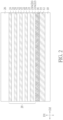
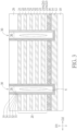
- FIGs. 2-8 are schematic drawings illustrating the manufacturing method of the 3D memory device in this embodiment.
- a manufacturing method of a 3D memory device is provided, and the manufacturing method includes the following steps.
- a substrate 10 is provided, and an alternating dielectric stack 20 is formed on the substrate 10.
- the alternating dielectric stack 20 may include a plurality of dielectric layers 22 and a plurality of sacrificial layers 24 alternately stacked in a vertical direction D1 perpendicular to a surface of the substrate 10, but not limited thereto.
- the dielectric layers 22 and the sacrificial layers 24 in the alternating dielectric stack 20 may include dielectric materials including, but not limited to, silicon oxide, silicon nitride, silicon oxynitride, or any combination thereof.
- the material composition of the dielectric layer 22 may be different from the material composition of the sacrificial layer 24 for providing the required etching selectivity in the step of forming a staircase structure (not shown) at least on one lateral side of the alternating dielectric stack 20.
- each of the dielectric layers 22 may be a silicon oxide layer
- each of the sacrificial layers 24 may be a silicon nitride layer, but not limited thereto.
- the total numbers of the dielectric layers 22 and the sacrificial layers 24 in the dielectric stack may be 32 or 64, but not limited thereto.
- the vertical direction D1 may also be regarded as a thickness direction of the substrate 10, and the substrate 10 may include silicon (e.g., monocrystalline silicon, polycrystalline silicon), silicon germanium (SiGe), silicon carbide (SiC), gallium nitride (GaN), indium phosphide (InP), gallium arsenide (GaAs), germanium (Ge), silicon on insulator (SOI), germanium on insulator (GOI), or any suitable combination thereof.
- a first doped region 12 and a protection layer 14 may be formed before the step of forming the alternating dielectric stack 20, but not limited thereto.
- the first doped region 12 may be a doped well formed in the substrate 10 by an implantation process, and the protection layer 14 may be formed on the substrate 10 before the implantation process.
- the protection layer 14 may include an oxide layer formed by performing an oxidation treatment to the substrate 10 before forming the first doped region 12.
- a dummy layer 16 may be formed on the substrate 10 before forming the alternating dielectric stack 20, and the dummy layer 16 may be located between the substrate 10 and the alternating dielectric stack 20 in the vertical direction D1.
- the dummy layer 16 may be located between the protection layer 14 and the alternating dielectric stack 20 in the vertical direction D1.
- the dummy layer 16 may include polysilicon, amorphous silicon, or other suitable sacrificial materials different from the material of the dielectric layer 22 and the material of the sacrificial layer 24.
- one or more vertical structures 30 may be formed penetrating the alternating dielectric stack 20 in the vertical direction D1.
- the vertical structure 30 may penetrate the alternating dielectric stack 20, the dummy layer 16, and the protection layer 14 in the vertical direction D1 for being partly disposed in the first doped region 12, and the vertical structure 30 does not penetrate the first doped region 12 preferably, but not limited thereto. Therefore, a lower portion of the vertical structure 30 may be located below the alternating dielectric stack 20 in the vertical direction D1 and be surrounded by the dummy layer 16 in a horizontal direction D2 orthogonal to the vertical direction D1.
- a first cap layer 26 may be formed on the alternating dielectric stack 20 before the step of forming the vertical structures 30, and each of the vertical structures 30 may further penetrate the first cap layer 26 in the vertical direction D1.
- the first cap layer 26 may include an oxide layer, such as a silicon oxide layer, or other suitable insulation materials.
- the vertical structure 30 may include a vertical memory structure, such as a NAND string or other suitable vertical memory structures.
- the vertical structure 30 may include a barrier layer 31, a storage layer 32, a tunneling layer 33, a semiconductor layer 34, a filling structure 35, and a conductive structure 36.
- the vertical structure 30 may be formed by forming a channel hole vertically penetrating the first cap layer 26, the alternating dielectric stack 20, the dummy layer 16, and the protection layer 14 and partly located in the first doped region 12; forming the barrier layer 31 conformally on the surface of the channel hole; forming the storage layer 32 conformally on the barrier layer 32; forming the tunneling layer 33 conformally on the storage layer 32; forming the semiconductor layer 34 conformally on the tunneling layer 33; forming the filling structure 35 on the semiconductor layer 34; and forming the conductive structure 36 on the filling structure 35. Therefore, the semiconductor layer 34 may surround the filling structure 35 in the horizontal direction D2, and the tunneling layer 33, the storage layer 32, and the barrier layer 31 may surround the semiconductor layer 34 in the horizontal direction D2.
- the barrier layer 31, the storage layer 32, the tunneling layer 33, the semiconductor layer 34, the filling structure 35, and the conductive structure 36 may be respectively formed by one or more thin film deposition processes, such as ALD, CVD, PVD, any other suitable processes, or any combination thereof, and one or more planarization processes and/or etching back process may be performed for forming the vertical structures 30, but not limited thereto.
- the barrier layer 31 may be used for blocking the outflow of the electronic charges, and the barrier layer 31 may include a silicon oxide layer or a combination of silicon oxide/silicon nitride/silicon oxide (ONO) layers. In some embodiments, the barrier layer 31 may include high dielectric constant (high-k) dielectrics (e.g., aluminum oxide), but not limited thereto. Electrons or holes from the semiconductor layer 34 may tunnel to the storage layer 32 through the tunneling layer 33. The storage layer 32 may be used for storing electronic charges (electrons or holes) for memory operation.
- the storage or removal of charge in the storage layer 32 can impact the on/off state and/or a conductance of the semiconductor channel, and the storage layer 32 may include one or more films of materials including, but are not limited to, silicon nitride, silicon oxynitride, a combination of silicon oxide and silicon nitride, or any combination thereof.
- the tunneling layer 33 may be used for tunneling electronic charges (electrons or holes), and the tunneling layer 33 may include dielectric materials including, but not limited to, silicon oxide, silicon nitride, silicon oxynitride, or any combination thereof.
- the semiconductor layer 34 may include amorphous silicon, polysilicon, or other suitable semiconductor materials.
- the filling structure 35 may include oxide or other suitable insulation materials, and the filling structure 35 may include one or more air voids V, but not limited thereto.
- the conductive structure 36 may be formed on a recess above the filling structure 35, and the conductive structure 36 may include polysilicon or other suitable conductive materials. It is worth noting that the vertical structure 30 of the present disclosure is not limited to the components and the manufacturing approaches described above. In some embodiments, the vertical structure 30 may include other components and/or be formed by other manufacturing approaches.
- a bottom dielectric layer 22A of the alternating dielectric stack 20 is removed.
- the bottom dielectric layer 22A is the bottommost dielectric layer 22 in the alternating dielectric stack 20, and the bottom dielectric layer 22A may directly contact the dummy layer 16 in some embodiments, but not limited thereto.
- one or more slits 44 may be formed vertically penetrating the first cap layer 26 and the alternating dielectric stack 20 for exposing a part of the dummy layer 16 after the step of forming the vertical structures 30 and before the step of removing the bottom dielectric layer 22A.
- a second cap layer 42 may be formed on the first cap layer 26 and the vertical structures 30 before the step of forming the slit 44, and the slit 44 may further penetrate the second cap layer 42 in the vertical direction D1.
- the second cap layer 42 may include an oxide layer, such as a silicon oxide layer, or other suitable insulation materials.
- the bottom dielectric layer 22A may be removed by one or more etching processes via the slit 44.
- the dummy layer 16 may be removed by an etching process (such as a suitable wet etching process) before the step of removing the bottom dielectric layer 22A and after the step of forming the vertical structures 30.
- a part of the vertical structure 30 may be exposed, and one or more etching processes may be performed to remove a part of the barrier layer 31, a part of the storage layer 32, and a part of the tunneling layer 33 for exposing a part of the semiconductor layer 34 of the vertical structure 30.
- an opening 46 may be formed laterally penetrating (e.g. in the horizontal direction D2) the barrier layer 31, the storage layer 32, and the tunneling layer 33 for exposing a part of the semiconductor layer 34 below the alternating dielectric stack 20, and the opening 46 may be located between the alternating dielectric stack 20 and the first doped region 12 in the vertical direction D1.
- the protection layer 14 and the bottom surface of the bottom dielectric layer 22A may also be exposed after the step of removing the dummy layer 16.
- the protection layer 14, a part of the barrier layer 31, and a part of the bottom dielectric layer 22A may be removed by an etching process, such as a wet etching process, especially when the materials of the protection layer 14, the barrier layer 31, and the bottom dielectric layer 22A are similar to one another.
- the remaining bottom dielectric layer 22A may be removed subsequently by an etching process for removing the tunneling layer 33.
- the thickness of the bottom dielectric layer 22A may be less than the thickness of each of other dielectric layers 22 in the alternating dielectric stack 20 preferably, but not limited thereto.
- the thickness of the bottom sacrificial layer 24A may be larger than the thickness of each of other sacrificial layers 24 in the alternating dielectric stack 20 preferably for providing space for forming a replacement of the bottom dielectric layer 22A subsequently, but not limited thereto.
- a gap 48 such as an air gap, may be formed between the first doped region 12 and the alternating dielectric stack 20 in the vertical direction D1.
- an epitaxial layer 50 is formed between the substrate 10 and the alternating dielectric stack 20 after removing the bottom dielectric layer 22A.
- the epitaxial layer 50 may be a polysilicon layer formed on the first doped region 12 by a selective epitaxial growth (SEG) process, and the epitaxial layer 50 may grow at the surface of the first doped region 12 and/or the surface of the semiconductor layer 34 exposed by the opening 46, but not limited thereto.
- the epitaxial layer 50 may include other suitable epitaxial materials and/or be formed by other suitable processes in some embodiments.
- the epitaxial layer 50 may directly contact and be electrically connected with the semiconductor layer 34 of the vertical structure 30, such as the part of the semiconductor layer 34 exposed by the opening 46, but not limited thereto.
- the epitaxial layer 50 may become a part of the first doped region 12 because the dopant (such as boron) in the first doped region 12 may diffuse into the epitaxial layer 50.
- an insulating layer 52 is formed on the epitaxial layer 50.
- the insulating layer 52 may be located between the epitaxial layer 50 and the dielectric layers 22 of the alternating dielectric stack 20 in the vertical direction D1.
- the insulating layer 52 may be regarded as a replacement of the bottom dielectric layer in the alternating dielectric stack 20.
- the insulating layer 52 may include an oxide layer, such as a silicon oxide layer, or other suitable insulating materials.
- the insulating layer 52 may be formed by performing an oxidation process to the epitaxial layer 50, and the oxidation process may include a chemical oxidation treatment, a thermal oxidation treatment, or other suitable oxidation approaches.
- the epitaxial layer 50 may be separated from the alternating dielectric stack 20 by the gap 48 before forming the insulating layer 52.
- at least a part of the epitaxial layer 50 may be connected with the bottom sacrificial layer 24A of the alternating dielectric stack 20.
- the epitaxial layer 50 may include a protruding part 50P located between the insulating layer 52 and the vertical structure 30 in the horizontal direction D2, and a top surface of the epitaxial layer 50 (such as a topmost surface of the protruding part 50P) may be higher than a bottom surface of the insulating layer 52 in the vertical direction D1, but not limited thereto.
- the sacrificial layers 24 of the alternating dielectric stack 20 may be removed. In some embodiments, the sacrificial layers 24 may be removed before the step of forming the insulating layer 52 for avoiding influencing the oxidation process performed to the epitaxial layer 50.
- the sacrificial layers 24 may be removed after the step of forming the insulating layer 52 for controlling the thickness of the insulating layer 52.
- a recess 54 may be formed at the bottom of the slit 44 by removing a part of the insulating layer 52 and a part of the epitaxial layer 50, but not limited thereto.
- the sacrificial layers 24 in the alternating dielectric stack 20 may be replaced with conductive layers 62 so as to form an alternating conductive/dielectric stack 60 including the dielectric layers 22 and the conductive layers 62 alternately stacked in the vertical direction D1.
- the conductive layers 62 may be formed after the step of forming the insulating layer 52, and the insulating layer 52 may be regarded as a bottom dielectric layer in the alternating conductive/dielectric stack 60, but not limited thereto.
- a high-k dielectric layer and a barrier layer may be formed between the vertical structure 30 and each of the conductive layers 62.
- the conductive layers 62 may include conductive materials including, but not limited to, W, Co, Cu, Al, doped silicon, polysilicon, silicide, or any combination thereof.
- the conductive layers 62 may be formed by thin film deposition processes, such as CVD, ALD, any other suitable process. A part of the conductive layers 62 corresponding to the slit 44 may be removed, and a second doped region 56 may be formed in the epitaxial layer 50 under the recess 54, but not limited thereto.
- a source structure (not shown) may be formed in the slit 44 and connected with the second doped region 56.
- the vertical structure 30 is formed before the step of forming the epitaxial layer 50, and the influence of the vertical structure 30 and/or the step of forming the vertical structure 30 on the epitaxial layer 50 may be avoided accordingly.
- the process window of forming the vertical structure 30 may be improved because it is not necessary to consider the influence of the vertical structure 30 on the epitaxial growth condition of the epitaxial layer 50.
- the bottom dielectric layer of the alternating dielectric stack may be replaced by the insulating layer 52 formed on the epitaxial layer 50 for reducing defects at the interface between the epitaxial layer and the bottom dielectric layer of the alternating dielectric stack.
- the manufacturing yield and the electrical performance of the 3D memory device may be enhanced accordingly.
- a 3D memory device 101 may be formed by the manufacturing method described above.
- the 3D memory device 101 may include the substrate 10, the alternating conductive/dielectric stack 60, the epitaxial layer 50, and the vertical structures 30.
- the alternating conductive/dielectric stack 60 may be disposed on the substrate 10.
- the alternating conductive/dielectric stack 60 may include a plurality of the dielectric layers 22 and a plurality of the conductive layers 62 alternately stacked in the vertical direction D1, and the insulating layer 52 may be regarded as the bottom dielectric layer in the alternating conductive/dielectric stack 60.
- the epitaxial layer 50 may be disposed between the substrate 10 and the alternating conductive/dielectric stack 60 in the vertical direction D1.
- the vertical structure 30 may penetrate the alternating conductive/dielectric stack 60 in the vertical direction D1 for being partly disposed in the epitaxial layer 50.
- the epitaxial layer 50 may include the protruding part 50P disposed between the vertical structure 30 and the bottom dielectric layer (i.e. the insulating layer 52) of the alternating conductive/dielectric stack 60 in the horizontal direction D2.
- the bottom dielectric layer (i.e. the insulating layer 52) of the alternating conductive/dielectric stack 60 may surround the protruding part 50P of the epitaxial layer 50 in the horizontal direction D1.
- the top surface of the epitaxial layer 50 (such as the topmost surface of the protruding part 50P) may be higher than the bottom surface of the bottom dielectric layer (i.e. the insulating layer 52) in the vertical direction D1.
- the vertical structure 30 may include a vertical memory structure, such as a NAND string including the barrier layer 31, the storage layer 32, the tunneling layer 33, the semiconductor layer 34, the filling structure 35, and the conductive structure 36, but not limited thereto.
- the semiconductor layer 34 may surround the filling structure 35 in the horizontal direction D2, and the tunneling layer 33, the storage layer 32, and the barrier layer 31 may surround the semiconductor layer 34 in the horizontal direction D2.
- the epitaxial layer 50 may contact a part of the semiconductor layer 34 disposed under the alternating conductive/dielectric stack 60 for being electrically connected with the semiconductor layer 34 of the vertical structure 30.
- the protruding part 50P of the epitaxial layer 50 may surround and contact a part of the semiconductor layer 34 of the vertical structure 30.
- the epitaxial layer 50 may include a doped well region on the substrate 10.
- the epitaxial layer 50 may be regarded as a lateral extending channel structure of a bottom select gate (BSG) transistor in a NAND memory structure, and the semiconductor layer 34 of the vertical structure 30 may be electrically connected to the doped well (e.g. the first doped region 12) via the epitaxial layer 50 for avoiding some operation issues of the 3D memory device 101, such as hole erase operation induced by gate induced drain leakage (GIDL).
- GIDL gate induced drain leakage
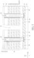
- FIG. 9 is a schematic drawing illustrating a 3D memory device 102 according to a second embodiment of the present invention
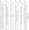
- FIG. 10 is a flowchart of a manufacturing method of the 3D memory device 102 in this embodiment.
- the difference between the 3D memory device 102 and the 3D memory device in the first embodiment described above is that the 3D memory device 102 may further include another alternating conductive/dielectric stack 70 disposed on the alternating conductive/dielectric stack 60.
- the alternating conductive/dielectric stack 60 may be regarded as a first alternating conductive/dielectric stack
- the alternating conductive/dielectric stack 70 may be regarded as a second alternating conductive/dielectric stack
- the 3D memory device 102 may be regarded as a dual-deck 3D memory structure.
- the alternating conductive/dielectric stack 70 may include a plurality of conductive layers 72 and a plurality of dielectric layers 72 alternately stacked in the vertical direction D1.
- the material of the conductive layer 72 may be similar to that of the conductive layer 62, and the material of the dielectric layer 74 may be similar to that of the dielectric layer 22, but not limited thereto.
- the vertical structure 30 in the 3D memory device 102 may vertically penetrate the alternating conductive/dielectric stack 70 and the alternating conductive/dielectric stack 60.
- a lower portion of the vertical structure 30 may be disposed in a first channel hole H1 penetrating the alternating conductive/dielectric stack 60
- a upper portion of the vertical structure 30 may be disposed in a second channel hole H2 penetrating the alternating conductive/dielectric stack 70.
- the first channel hole H1 and the second channel hole H2 may be formed separately, and the shape and/or the size of the second channel hole H2 may be different from that of the first channel hole H1, but not limited thereto.
- the second channel hole H2 may further penetrates a third cap layer 76 disposed on the alternating conductive/dielectric stack 70, and a fourth cap layer 78 may be disposed on the third cap layer 76 and the vertical structure 30.
- the manufacturing method of the 3D memory device 102 may include but is not limited to the following steps.
- a first alternating dielectric stack may be formed on the substrate 10
- a second alternating dielectric stack may be formed on the first alternating dielectric stack.
- the structure and the material composition of the first alternating dielectric stack and the second alternating dielectric stack may be similar to the alternating dielectric stack shown in FIG. 2 of the first embodiments described above.
- the vertical structure 30 may be formed penetrating the first alternating dielectric stack and the second alternating dielectric stack.
- the first channel hole H1 penetrating the first alternating dielectric stack may be formed before the step of forming the second alternating dielectric stack, but not limited thereto.
- steps S23-S25 are carried out.
- the bottom dielectric layer of the first alternating dielectric stack is removed, the epitaxial layer 50 is formed between the substrate 10 and the first alternating dielectric stack, and the insulating layer 52 is formed on the epitaxial layer 50.
- the details of the steps S23-S25 may be similar to those of the steps S13-S15 in FIGs. 1 and 4-7 of the first embodiment described above and will not be redundantly described.
- step S26 sacrificial layers in the first alternating dielectric stack and the second alternating dielectric stack may be replaced with conductive layers (such as the conductive layers 62 and the conductive layers 72) for forming the alternating conductive/dielectric stack 60 and the alternating conductive/dielectric stack 70 respectively.
- conductive layers such as the conductive layers 62 and the conductive layers 72
- the vertical structure 30 may be formed before the step of forming the epitaxial layer 50, and the influence of the vertical structure 30 and/or the step of forming the vertical structure 30 on the epitaxial layer 50 may be avoided accordingly.
- the process window of forming the vertical structure 30, such as the window of the overlay condition between the first channel hole H1 and the second channel hole H2, may be improved because it is not necessary to consider the influence of the vertical structure 30 and/or the step of forming the vertical structure 30 on the epitaxial growth condition of the epitaxial layer 50.
- the manufacturing yield of the 3D memory device may be enhanced accordingly.
- the vertical structure may be formed before the step of forming the epitaxial layer for avoiding the influence of the vertical structure and/or the process of forming the vertical structure on the epitaxial layer.
- the process window of forming the vertical structure may be improved because it is not necessary to consider the influence of the vertical structure and/or the process of forming the vertical structure on the epitaxial growth condition of the epitaxial layer.
- the bottom dielectric layer of the alternating dielectric stack may be replaced by the insulating layer formed on the epitaxial layer for reducing defects at the interface between the epitaxial layer and the bottom dielectric layer of the alternating dielectric stack.
- the manufacturing yield and the electrical performance of the 3D memory device may be enhanced accordingly.
- the manufacturing yield may be further improved because the overlay window between the channel holes may be enlarged by the manufacturing method of the present disclosure.
Landscapes
- Semiconductor Memories (AREA)
- Non-Volatile Memory (AREA)
Claims (12)
- Herstellungsverfahren für eine dreidimensionale (3D) Speichervorrichtung (101, 102), umfassend:Ausbilden eines alternierenden dielektrischen Stapels (20) auf einem Substrat (10);Bilden einer vertikalen Struktur (30), die den alternierenden dielektrischen Stapel (20) in einer vertikalen Richtung senkrecht zu einer Oberfläche des Substrats (10) durchdringt;Entfernen einer unteren dielektrischen Schicht (22A) des alternierenden dielektrischen Stapels (20);Bilden einer Epitaxieschicht (50) zwischen dem Substrat (10) und dem alternierenden dielektrischen Stapel (20) nach dem Entfernen der unteren dielektrischen Schicht (22A); undBilden einer Isolierschicht (52) auf der Epitaxieschicht (50), wobei die Isolierschicht (52) zwischen der Epitaxieschicht (50) und dem alternierenden dielektrischen Stapel (20) angeordnet ist, wobei die Isolierschicht (52) durch Ausführen eines Oxidationsprozesses an der Epitaxieschicht (50) gebildet wird,wobei die Epitaxieschicht (50) von dem alternierenden dielektrischen Stapel (20) durch einen Spalt (48) getrennt wird, bevor die Isolierschicht (52) gebildet wird,wobei ein Schlitz (44) gebildet wird, der den alternierenden dielektrischen Stapel (20) vertikal durchdringt,wobei eine Ausnehmung (54) am Boden des Schlitzes (44) durch Entfernen eines Teils der Isolierschicht (52) und eines Teils der Epitaxieschicht (50) gebildet wird, wobei ein zweiter dotierter Bereich (56) in der Epitaxieschicht (50) unter der Ausnehmung (54) gebildet wird,wobei die Epitaxieschicht (50) einen vorstehenden Teil (50P) aufweist, der zwischen der Isolierschicht (52) und der vertikalen Struktur (30) in einer horizontalen Richtung orthogonal zur vertikalen Richtung angeordnet ist.
- Herstellungsverfahren für die 3D-Speichervorrichtung (101, 102) nach Anspruch 1, wobei eine obere Oberfläche der Epitaxieschicht (50) höher ist als eine untere Oberfläche der Isolierschicht (52) in der vertikalen Richtung.
- Herstellungsverfahren für die 3D-Speichervorrichtung (101, 102) nach Anspruch 1, ferner umfassend:
Bilden eines dotierten Bereichs (12, 56) in dem Substrat (10) vor dem Bilden des alternierenden dielektrischen Stapels (20), wobei die Epitaxieschicht (50) auf dem dotierten Bereich (12, 56) durch ein selektives Epitaxiewachstumsverfahren (SEG) gebildet wird. - Herstellungsverfahren für die 3D-Speichervorrichtung (101, 102) nach Anspruch 1, wobei ein Teil der vertikalen Struktur (30) unterhalb des alternierenden dielektrischen Stapels (20) angeordnet ist, die vertikale Struktur (30) eine Halbleiterschicht (34) und eine die Halbleiterschicht (34) umgebende Speicherschicht (32) umfasst, und das Herstellungsverfahren ferner umfasst: Entfernen eines Teils der Speicherschicht (32), um einen Teil der Halbleiterschicht (34) unterhalb des alternierenden dielektrischen Stapels (20) freizulegen, bevor die Epitaxieschicht (50) gebildet wird, wobei die Epitaxieschicht (50) mit dem freigelegten Teil der Halbleiterschicht (34) verbunden wird.
- Herstellungsverfahren für die 3D-Speichervorrichtung (101, 102) nach Anspruch 1, ferner umfassend:Bilden einer Dummy-Schicht (16) auf dem Substrat (10) vor dem Bilden des alternierenden dielektrischen Stapels (20), wobei die Dummy-Schicht (16) zwischen dem Substrat (10) und dem alternierenden dielektrischen Stapel (20) in der vertikalen Richtung angeordnet ist; undEntfernen der Dummy-Schicht (16) vor dem Bilden der Epitaxieschicht (50), wobei das Herstellungsverfahren der 3D-Speichervorrichtung (101, 102) insbesondere weiterhin umfasst:
Freilegen eines Teils der Dummy-Schicht (16) vor dem Entfernen der Dummy-Schicht (16) nach dem Bilden der vertikalen Struktur (30). - Herstellungsverfahren für die 3D-Speichervorrichtung (101, 102) nach Anspruch 1, wobei der alternierende dielektrische Stapel (20) eine Vielzahl von dielektrischen Schichten (22, 72) und eine Vielzahl von Opferschichten (24) umfasst, die abwechselnd in der vertikalen Richtung gestapelt sind.
- Herstellungsverfahren für die 3D-Speichervorrichtung (101, 102) nach Anspruch 6, ferner umfassend:
Ersetzen der Opferschichten (24) durch leitende Schichten (62, 72), um einen alternierenden leitenden/dielektrischen Stapel (60, 70) zu bilden. - Herstellungsverfahren für die 3D-Speichervorrichtung (101, 102) nach Anspruch 1, wobei die Dicke der unteren dielektrischen Schicht (22A) geringer ist als die Dicke jeder der anderen dielektrischen Schichten (22, 72) in dem alternierenden dielektrischen Stapel (20).
- Eine dreidimensionale (3D) Speichervorrichtung (101, 102), umfassend:ein Substrat (10);einen alternierenden leitenden/dielektrischen Stapel (60, 70), der auf dem Substrat (10) angeordnet ist, wobei der alternierende leitende/dielektrische Stapel (60, 70) eine Vielzahl von dielektrischen Schichten (22, 72) und eine Vielzahl von leitenden Schichten (62, 72) umfasst, die abwechselnd in einer vertikalen Richtung senkrecht zu einer Oberfläche des Substrats (10) gestapelt sind;eine Epitaxieschicht (50), die zwischen dem Substrat (10) und dem alternierenden leitenden/dielektrischen Stapel (60, 70) in der vertikalen Richtung angeordnet ist; undeine vertikale Struktur (30), die den abwechselnd leitenden/dielektrischen Stapel (60, 70) in der vertikalen Richtung durchdringt, um teilweise in der Epitaxieschicht (50) angeordnet zu sein, wobei die Epitaxieschicht (50) einen vorstehenden Teil (50P) umfasst, der zwischen der vertikalen Struktur (30) und einer Isolierschicht (52) in einer horizontalen Richtung orthogonal zu der vertikalen Richtung angeordnet ist,wobei die Isolierschicht (52) die untere dielektrische Schicht (22A) des abwechselnd leitenden/dielektrischen Schichtstapels ist,wobei die Isolierschicht (52) eine Oxidschicht enthält,wobei ein Schlitz (44) den alternierenden dielektrischen Stapel (20) vertikal durchdringt,wobei eine Vertiefung (54) am Boden des Schlitzes (44) angeordnet ist,wobei in der Epitaxieschicht (50) unter der Ausnehmung (54) ein zweiter dotierter Bereich (56) angeordnet ist.
- 3D- Speichervorrichtung (101, 102) nach Anspruch 9, wobei die untere dielektrische Schicht (22A) des abwechselnd leitenden/dielektrischen Stapels (60, 70) den vorstehenden Teil (50P) der Epitaxieschicht (50) in der horizontalen Richtung umgibtoder wobei eine obere Oberfläche der Epitaxieschicht (50) höher ist als eine untere Oberfläche der unteren dielektrischen Schicht (22A) in der vertikalen Richtungoder wobei die Epitaxieschicht (50) einen dotierten Muldenbereich (12, 56) auf dem Substrat (10) umfasst.
- 3D-Speichervorrichtung (101, 102) nach Anspruch 10, wobei die vertikale Struktur (30) eine Halbleiterschicht (34) und eine die Halbleiterschicht (34) umgebende Speicherschicht (32) umfasst.
- 3D- Speichervorrichtung (101, 102) nach Anspruch 11, wobei die Epitaxieschicht (50) die Halbleiterschicht (34) der vertikalen Struktur (30) kontaktiert
oder wobei der vorstehende Teil (50P) der Epitaxieschicht (50) die Halbleiterschicht (34) der vertikalen Struktur (30) umgibt und kontaktiert.
Applications Claiming Priority (1)
| Application Number | Priority Date | Filing Date | Title |
|---|---|---|---|
| PCT/CN2019/070871 WO2020142904A1 (en) | 2019-01-08 | 2019-01-08 | Three-dimensional memory device and manufacturing method thereof |
Publications (3)
| Publication Number | Publication Date |
|---|---|
| EP3853902A1 EP3853902A1 (de) | 2021-07-28 |
| EP3853902A4 EP3853902A4 (de) | 2022-05-11 |
| EP3853902B1 true EP3853902B1 (de) | 2024-03-06 |
Family
ID=66938493
Family Applications (1)
| Application Number | Title | Priority Date | Filing Date |
|---|---|---|---|
| EP19909369.1A Active EP3853902B1 (de) | 2019-01-08 | 2019-01-08 | Dreidimensionale speichervorrichtung und herstellungsverfahren dafür |
Country Status (7)
| Country | Link |
|---|---|
| US (3) | US10854628B2 (de) |
| EP (1) | EP3853902B1 (de) |
| JP (1) | JP7234369B2 (de) |
| KR (3) | KR20250114559A (de) |
| CN (3) | CN109891588B (de) |
| TW (1) | TWI691059B (de) |
| WO (1) | WO2020142904A1 (de) |
Families Citing this family (23)
| Publication number | Priority date | Publication date | Assignee | Title |
|---|---|---|---|---|
| CN110364536B (zh) * | 2019-07-23 | 2020-06-26 | 长江存储科技有限责任公司 | 三维存储器的制造方法以及三维存储器 |
| CN111223872B (zh) * | 2020-01-17 | 2023-04-07 | 长江存储科技有限责任公司 | 一种3d nand存储器及其制造方法 |
| KR102824041B1 (ko) * | 2020-02-19 | 2025-06-23 | 에스케이하이닉스 주식회사 | 반도체 장치 및 반도체 장치의 제조 방법 |
| KR102666864B1 (ko) * | 2020-02-26 | 2024-05-20 | 양쯔 메모리 테크놀로지스 씨오., 엘티디. | 메모리 디바이스 및 그 형성 방법 |
| WO2021184176A1 (en) | 2020-03-17 | 2021-09-23 | Yangtze Memory Technologies Co., Ltd. | Three-dimensional memory devices and fabricating methods thereof |
| WO2021184328A1 (en) * | 2020-03-20 | 2021-09-23 | Yangtze Memory Technologies Co., Ltd. | Three-dimensional memory device and fabrication method |
| KR102647874B1 (ko) * | 2020-03-20 | 2024-03-13 | 양쯔 메모리 테크놀로지스 씨오., 엘티디. | 3차원 메모리 디바이스 및 그 제조 방법 |
| WO2021208195A1 (en) | 2020-04-14 | 2021-10-21 | Yangtze Memory Technologies Co., Ltd. | Methods for forming three-dimensional memory devices |
| CN111430364B (zh) * | 2020-04-22 | 2023-08-08 | 长江存储科技有限责任公司 | 半导体器件结构及其制备方法 |
| CN111540749B (zh) * | 2020-04-23 | 2021-04-13 | 长江存储科技有限责任公司 | 三维存储器及其形成方法 |
| CN113644075B (zh) * | 2020-04-27 | 2024-02-27 | 长江存储科技有限责任公司 | 三维存储器件及用于形成其的方法 |
| CN111415942B (zh) * | 2020-05-14 | 2023-06-09 | 长江存储科技有限责任公司 | 三维存储器的形成方法 |
| CN112585754B (zh) * | 2020-05-27 | 2024-07-19 | 长江存储科技有限责任公司 | 用于形成三维存储器件的方法 |
| WO2021237489A1 (en) | 2020-05-27 | 2021-12-02 | Yangtze Memory Technologies Co., Ltd. | Methods for forming three-dimensional memory devices |
| WO2021237488A1 (en) | 2020-05-27 | 2021-12-02 | Yangtze Memory Technologies Co., Ltd. | Three-dimensional memory devices |
| CN112018121B (zh) * | 2020-09-01 | 2023-10-24 | 长江存储科技有限责任公司 | 半导体器件及其制作方法 |
| CN114649260B (zh) * | 2020-12-18 | 2025-02-18 | 富泰华工业(深圳)有限公司 | 三维半导体结构的制作方法及三维半导体结构 |
| CN112786606B (zh) * | 2021-01-14 | 2023-04-28 | 长江存储科技有限责任公司 | 一种三维存储器件及其制造方法 |
| US11758724B2 (en) * | 2021-02-04 | 2023-09-12 | Macronix International Co., Ltd. | Memory device with memory string comprising segmented memory portions and method for fabricating the same |
| US20220285385A1 (en) * | 2021-03-03 | 2022-09-08 | Macronix International Co., Ltd. | Memory device and method for fabricating the same |
| CN114400230A (zh) * | 2021-12-30 | 2022-04-26 | 长江存储科技有限责任公司 | 存储器的制备方法及存储器 |
| CN114497065A (zh) * | 2022-02-10 | 2022-05-13 | 长江存储科技有限责任公司 | 三维存储器、制备方法以及存储系统 |
| KR102753493B1 (ko) * | 2023-06-23 | 2025-01-10 | 한양대학교 산학협력단 | 다층 커패시터 수평 전극들을 포함하는 3차원 메모리 및 그 제조 방법 |
Citations (2)
| Publication number | Priority date | Publication date | Assignee | Title |
|---|---|---|---|---|
| US20170025421A1 (en) * | 2015-05-08 | 2017-01-26 | Sandisk Technologies Llc | Three-dimensional junction memory device and method reading thereof using hole current detection |
| US20180323213A1 (en) * | 2017-02-28 | 2018-11-08 | Toshiba Memory Corporation | Semiconductor device and method for manufacturing same |
Family Cites Families (30)
| Publication number | Priority date | Publication date | Assignee | Title |
|---|---|---|---|---|
| JP4772656B2 (ja) * | 2006-12-21 | 2011-09-14 | 株式会社東芝 | 不揮発性半導体メモリ |
| FR2955203B1 (fr) * | 2010-01-14 | 2012-03-23 | Soitec Silicon On Insulator | Cellule memoire dont le canal traverse une couche dielectrique enterree |
| TWI442551B (zh) * | 2010-03-04 | 2014-06-21 | Macronix Int Co Ltd | 記憶體元件及其製造方法 |
| US9275909B2 (en) | 2013-08-12 | 2016-03-01 | Micron Technology, Inc. | Methods of fabricating semiconductor structures |
| US10141322B2 (en) * | 2013-12-17 | 2018-11-27 | Intel Corporation | Metal floating gate composite 3D NAND memory devices and associated methods |
| KR20160020210A (ko) * | 2014-08-13 | 2016-02-23 | 에스케이하이닉스 주식회사 | 반도체 장치 및 그 제조 방법 |
| KR20170014036A (ko) * | 2015-07-28 | 2017-02-08 | 삼성전자주식회사 | 반도체 장치 |
| US9401371B1 (en) | 2015-09-24 | 2016-07-26 | Macronix International Co., Ltd. | Sacrificial spin-on glass for air gap formation after bl isolation process in single gate vertical channel 3D NAND flash |
| US9911748B2 (en) * | 2015-09-28 | 2018-03-06 | Sandisk Technologies Llc | Epitaxial source region for uniform threshold voltage of vertical transistors in 3D memory devices |
| KR102485088B1 (ko) * | 2015-11-10 | 2023-01-05 | 삼성전자주식회사 | 수직형 메모리 장치 및 그 제조 방법 |
| US9917100B2 (en) * | 2015-11-20 | 2018-03-13 | Sandisk Technologies Llc | Three-dimensional NAND device containing support pedestal structures for a buried source line and method of making the same |
| US9831266B2 (en) * | 2015-11-20 | 2017-11-28 | Sandisk Technologies Llc | Three-dimensional NAND device containing support pedestal structures for a buried source line and method of making the same |
| CN105470260B (zh) * | 2015-12-03 | 2018-09-18 | 中国科学院微电子研究所 | 三维半导体器件及其制造方法 |
| US9659956B1 (en) * | 2016-01-06 | 2017-05-23 | Sandisk Technologies Llc | Three-dimensional memory device containing source select gate electrodes with enhanced electrical isolation |
| US9704872B1 (en) * | 2016-01-07 | 2017-07-11 | Micron Technology, Inc. | Memory device and fabricating method thereof |
| KR102549452B1 (ko) * | 2016-03-31 | 2023-06-30 | 에스케이하이닉스 주식회사 | 반도체 장치 및 그 제조 방법 |
| US9853049B2 (en) * | 2016-04-21 | 2017-12-26 | Samsung Electronics Co., Ltd. | Memory devices having common source lines including layers of different materials |
| US9824966B1 (en) * | 2016-08-12 | 2017-11-21 | Sandisk Technologies Llc | Three-dimensional memory device containing a lateral source contact and method of making the same |
| CN107768381B (zh) * | 2016-08-17 | 2021-11-09 | 上海新昇半导体科技有限公司 | 一种纳米管存储器结构及其制备方法 |
| KR102682890B1 (ko) * | 2017-02-27 | 2024-07-05 | 삼성전자주식회사 | 수직형 메모리 장치 |
| JP2018142654A (ja) * | 2017-02-28 | 2018-09-13 | 東芝メモリ株式会社 | 半導体装置及びその製造方法 |
| TWI632645B (zh) * | 2017-03-09 | 2018-08-11 | 旺宏電子股份有限公司 | 立體記憶體元件及其製作方法 |
| KR20180137264A (ko) * | 2017-06-16 | 2018-12-27 | 에스케이하이닉스 주식회사 | 반도체 장치 및 그 제조방법 |
| US10438964B2 (en) * | 2017-06-26 | 2019-10-08 | Sandisk Technologies Llc | Three-dimensional memory device having direct source contact and metal oxide blocking dielectric and method of making thereof |
| CN107731671B (zh) * | 2017-08-24 | 2019-11-12 | 长江存储科技有限责任公司 | 改善硅外延生长中离子注入硼元素扩散的工艺 |
| US10797067B2 (en) | 2017-08-31 | 2020-10-06 | Yangtze Memory Technologies Co., Ltd. | Three-dimensional memory device and fabricating method thereof |
| CN107564915B (zh) * | 2017-08-31 | 2018-11-16 | 长江存储科技有限责任公司 | 一种3d nand存储器件及其制造方法 |
| CN108565266B (zh) * | 2018-06-04 | 2023-10-27 | 长江存储科技有限责任公司 | 形成三维存储器的方法以及三维存储器 |
| CN208208759U (zh) * | 2018-06-04 | 2018-12-07 | 长江存储科技有限责任公司 | 三维存储器 |
| CN113345910B (zh) * | 2018-08-14 | 2024-02-27 | 长江存储科技有限责任公司 | 3d存储器中的堆叠连接件及其制造方法 |
-
2019
- 2019-01-08 EP EP19909369.1A patent/EP3853902B1/de active Active
- 2019-01-08 KR KR1020257024132A patent/KR20250114559A/ko active Pending
- 2019-01-08 JP JP2021530979A patent/JP7234369B2/ja active Active
- 2019-01-08 KR KR1020217015914A patent/KR102675751B1/ko active Active
- 2019-01-08 CN CN201980000186.1A patent/CN109891588B/zh active Active
- 2019-01-08 CN CN202010417291.XA patent/CN111415944B/zh active Active
- 2019-01-08 WO PCT/CN2019/070871 patent/WO2020142904A1/en not_active Ceased
- 2019-01-08 KR KR1020247019431A patent/KR102840888B1/ko active Active
- 2019-03-04 TW TW108106968A patent/TWI691059B/zh active
- 2019-03-04 US US16/292,212 patent/US10854628B2/en active Active
- 2019-10-12 CN CN201910969274.4A patent/CN110676258B/zh active Active
-
2020
- 2020-07-22 US US16/935,223 patent/US11069712B2/en active Active
-
2021
- 2021-04-22 US US17/238,091 patent/US11515329B2/en active Active
Patent Citations (2)
| Publication number | Priority date | Publication date | Assignee | Title |
|---|---|---|---|---|
| US20170025421A1 (en) * | 2015-05-08 | 2017-01-26 | Sandisk Technologies Llc | Three-dimensional junction memory device and method reading thereof using hole current detection |
| US20180323213A1 (en) * | 2017-02-28 | 2018-11-08 | Toshiba Memory Corporation | Semiconductor device and method for manufacturing same |
Also Published As
| Publication number | Publication date |
|---|---|
| TW202027260A (zh) | 2020-07-16 |
| US20200350335A1 (en) | 2020-11-05 |
| CN109891588A (zh) | 2019-06-14 |
| KR20240096870A (ko) | 2024-06-26 |
| TWI691059B (zh) | 2020-04-11 |
| WO2020142904A1 (en) | 2020-07-16 |
| CN109891588B (zh) | 2020-06-26 |
| KR102840888B1 (ko) | 2025-07-30 |
| JP2022508289A (ja) | 2022-01-19 |
| US11515329B2 (en) | 2022-11-29 |
| CN110676258B (zh) | 2023-10-24 |
| CN110676258A (zh) | 2020-01-10 |
| CN111415944A (zh) | 2020-07-14 |
| US20210242238A1 (en) | 2021-08-05 |
| US10854628B2 (en) | 2020-12-01 |
| KR102675751B1 (ko) | 2024-06-14 |
| CN111415944B (zh) | 2021-04-27 |
| EP3853902A4 (de) | 2022-05-11 |
| US20200219897A1 (en) | 2020-07-09 |
| KR20250114559A (ko) | 2025-07-29 |
| KR20210087956A (ko) | 2021-07-13 |
| US11069712B2 (en) | 2021-07-20 |
| JP7234369B2 (ja) | 2023-03-07 |
| EP3853902A1 (de) | 2021-07-28 |
Similar Documents
| Publication | Publication Date | Title |
|---|---|---|
| EP3853902B1 (de) | Dreidimensionale speichervorrichtung und herstellungsverfahren dafür | |
| US12016180B2 (en) | Manufacturing method of three-dimensional memory device with improved RC delay | |
| US11758722B2 (en) | Three-dimensional memory device with deposited semiconductor plugs and methods for forming the same | |
| US20180226427A1 (en) | Integrated Structures Comprising Vertical Channel Material and Having Conductively-Doped Semiconductor Material Directly Against Lower Sidewalls of the Channel Material, and Methods of Forming Integrated Structures | |
| US11665905B2 (en) | Three-dimensional memory device and manufacturing method thereof | |
| WO2019100836A1 (en) | Three-dimensional memory structure and manufacturing method thereof | |
| US10756102B2 (en) | Three-dimensional memory structure and manufacturing method thereof | |
| US20260047191A1 (en) | Fets with dummy nanosheets |
Legal Events
| Date | Code | Title | Description |
|---|---|---|---|
| STAA | Information on the status of an ep patent application or granted ep patent |
Free format text: STATUS: THE INTERNATIONAL PUBLICATION HAS BEEN MADE |
|
| PUAI | Public reference made under article 153(3) epc to a published international application that has entered the european phase |
Free format text: ORIGINAL CODE: 0009012 |
|
| STAA | Information on the status of an ep patent application or granted ep patent |
Free format text: STATUS: REQUEST FOR EXAMINATION WAS MADE |
|
| 17P | Request for examination filed |
Effective date: 20210423 |
|
| AK | Designated contracting states |
Kind code of ref document: A1 Designated state(s): AL AT BE BG CH CY CZ DE DK EE ES FI FR GB GR HR HU IE IS IT LI LT LU LV MC MK MT NL NO PL PT RO RS SE SI SK SM TR |
|
| DAV | Request for validation of the european patent (deleted) | ||
| DAX | Request for extension of the european patent (deleted) | ||
| A4 | Supplementary search report drawn up and despatched |
Effective date: 20220413 |
|
| RIC1 | Information provided on ipc code assigned before grant |
Ipc: H01L 27/11582 20170101AFI20220407BHEP |
|
| STAA | Information on the status of an ep patent application or granted ep patent |
Free format text: STATUS: EXAMINATION IS IN PROGRESS |
|
| 17Q | First examination report despatched |
Effective date: 20221212 |
|
| REG | Reference to a national code |
Ref country code: DE Ref legal event code: R079 Free format text: PREVIOUS MAIN CLASS: H01L0027115780 Ipc: H10B0043270000 Ref country code: DE Ref legal event code: R079 Ref document number: 602019048028 Country of ref document: DE Free format text: PREVIOUS MAIN CLASS: H01L0027115780 Ipc: H10B0043270000 |
|
| GRAP | Despatch of communication of intention to grant a patent |
Free format text: ORIGINAL CODE: EPIDOSNIGR1 |
|
| STAA | Information on the status of an ep patent application or granted ep patent |
Free format text: STATUS: GRANT OF PATENT IS INTENDED |
|
| RIC1 | Information provided on ipc code assigned before grant |
Ipc: H10B 43/27 20230101AFI20230920BHEP |
|
| INTG | Intention to grant announced |
Effective date: 20231024 |
|
| GRAS | Grant fee paid |
Free format text: ORIGINAL CODE: EPIDOSNIGR3 |
|
| GRAA | (expected) grant |
Free format text: ORIGINAL CODE: 0009210 |
|
| STAA | Information on the status of an ep patent application or granted ep patent |
Free format text: STATUS: THE PATENT HAS BEEN GRANTED |
|
| AK | Designated contracting states |
Kind code of ref document: B1 Designated state(s): AL AT BE BG CH CY CZ DE DK EE ES FI FR GB GR HR HU IE IS IT LI LT LU LV MC MK MT NL NO PL PT RO RS SE SI SK SM TR |
|
| REG | Reference to a national code |
Ref country code: CH Ref legal event code: EP |
|
| REG | Reference to a national code |
Ref country code: IE Ref legal event code: FG4D |
|
| REG | Reference to a national code |
Ref country code: DE Ref legal event code: R096 Ref document number: 602019048028 Country of ref document: DE |
|
| P01 | Opt-out of the competence of the unified patent court (upc) registered |
Effective date: 20240228 |
|
| REG | Reference to a national code |
Ref country code: LT Ref legal event code: MG9D |
|
| PG25 | Lapsed in a contracting state [announced via postgrant information from national office to epo] |
Ref country code: LT Free format text: LAPSE BECAUSE OF FAILURE TO SUBMIT A TRANSLATION OF THE DESCRIPTION OR TO PAY THE FEE WITHIN THE PRESCRIBED TIME-LIMIT Effective date: 20240306 |
|
| REG | Reference to a national code |
Ref country code: NL Ref legal event code: MP Effective date: 20240306 |
|
| PG25 | Lapsed in a contracting state [announced via postgrant information from national office to epo] |
Ref country code: GR Free format text: LAPSE BECAUSE OF FAILURE TO SUBMIT A TRANSLATION OF THE DESCRIPTION OR TO PAY THE FEE WITHIN THE PRESCRIBED TIME-LIMIT Effective date: 20240607 |
|
| PG25 | Lapsed in a contracting state [announced via postgrant information from national office to epo] |
Ref country code: RS Free format text: LAPSE BECAUSE OF FAILURE TO SUBMIT A TRANSLATION OF THE DESCRIPTION OR TO PAY THE FEE WITHIN THE PRESCRIBED TIME-LIMIT Effective date: 20240606 Ref country code: HR Free format text: LAPSE BECAUSE OF FAILURE TO SUBMIT A TRANSLATION OF THE DESCRIPTION OR TO PAY THE FEE WITHIN THE PRESCRIBED TIME-LIMIT Effective date: 20240306 |
|
| PG25 | Lapsed in a contracting state [announced via postgrant information from national office to epo] |
Ref country code: ES Free format text: LAPSE BECAUSE OF FAILURE TO SUBMIT A TRANSLATION OF THE DESCRIPTION OR TO PAY THE FEE WITHIN THE PRESCRIBED TIME-LIMIT Effective date: 20240306 |
|
| PG25 | Lapsed in a contracting state [announced via postgrant information from national office to epo] |
Ref country code: RS Free format text: LAPSE BECAUSE OF FAILURE TO SUBMIT A TRANSLATION OF THE DESCRIPTION OR TO PAY THE FEE WITHIN THE PRESCRIBED TIME-LIMIT Effective date: 20240606 Ref country code: NO Free format text: LAPSE BECAUSE OF FAILURE TO SUBMIT A TRANSLATION OF THE DESCRIPTION OR TO PAY THE FEE WITHIN THE PRESCRIBED TIME-LIMIT Effective date: 20240606 Ref country code: LT Free format text: LAPSE BECAUSE OF FAILURE TO SUBMIT A TRANSLATION OF THE DESCRIPTION OR TO PAY THE FEE WITHIN THE PRESCRIBED TIME-LIMIT Effective date: 20240306 Ref country code: HR Free format text: LAPSE BECAUSE OF FAILURE TO SUBMIT A TRANSLATION OF THE DESCRIPTION OR TO PAY THE FEE WITHIN THE PRESCRIBED TIME-LIMIT Effective date: 20240306 Ref country code: GR Free format text: LAPSE BECAUSE OF FAILURE TO SUBMIT A TRANSLATION OF THE DESCRIPTION OR TO PAY THE FEE WITHIN THE PRESCRIBED TIME-LIMIT Effective date: 20240607 Ref country code: FI Free format text: LAPSE BECAUSE OF FAILURE TO SUBMIT A TRANSLATION OF THE DESCRIPTION OR TO PAY THE FEE WITHIN THE PRESCRIBED TIME-LIMIT Effective date: 20240306 Ref country code: ES Free format text: LAPSE BECAUSE OF FAILURE TO SUBMIT A TRANSLATION OF THE DESCRIPTION OR TO PAY THE FEE WITHIN THE PRESCRIBED TIME-LIMIT Effective date: 20240306 Ref country code: BG Free format text: LAPSE BECAUSE OF FAILURE TO SUBMIT A TRANSLATION OF THE DESCRIPTION OR TO PAY THE FEE WITHIN THE PRESCRIBED TIME-LIMIT Effective date: 20240306 |
|
| REG | Reference to a national code |
Ref country code: AT Ref legal event code: MK05 Ref document number: 1664811 Country of ref document: AT Kind code of ref document: T Effective date: 20240306 |
|
| PG25 | Lapsed in a contracting state [announced via postgrant information from national office to epo] |
Ref country code: SE Free format text: LAPSE BECAUSE OF FAILURE TO SUBMIT A TRANSLATION OF THE DESCRIPTION OR TO PAY THE FEE WITHIN THE PRESCRIBED TIME-LIMIT Effective date: 20240306 Ref country code: LV Free format text: LAPSE BECAUSE OF FAILURE TO SUBMIT A TRANSLATION OF THE DESCRIPTION OR TO PAY THE FEE WITHIN THE PRESCRIBED TIME-LIMIT Effective date: 20240306 |
|
| PG25 | Lapsed in a contracting state [announced via postgrant information from national office to epo] |
Ref country code: NL Free format text: LAPSE BECAUSE OF FAILURE TO SUBMIT A TRANSLATION OF THE DESCRIPTION OR TO PAY THE FEE WITHIN THE PRESCRIBED TIME-LIMIT Effective date: 20240306 |
|
| PG25 | Lapsed in a contracting state [announced via postgrant information from national office to epo] |
Ref country code: NL Free format text: LAPSE BECAUSE OF FAILURE TO SUBMIT A TRANSLATION OF THE DESCRIPTION OR TO PAY THE FEE WITHIN THE PRESCRIBED TIME-LIMIT Effective date: 20240306 |
|
| PG25 | Lapsed in a contracting state [announced via postgrant information from national office to epo] |
Ref country code: IS Free format text: LAPSE BECAUSE OF FAILURE TO SUBMIT A TRANSLATION OF THE DESCRIPTION OR TO PAY THE FEE WITHIN THE PRESCRIBED TIME-LIMIT Effective date: 20240706 |
|
| PG25 | Lapsed in a contracting state [announced via postgrant information from national office to epo] |
Ref country code: SM Free format text: LAPSE BECAUSE OF FAILURE TO SUBMIT A TRANSLATION OF THE DESCRIPTION OR TO PAY THE FEE WITHIN THE PRESCRIBED TIME-LIMIT Effective date: 20240306 Ref country code: PT Free format text: LAPSE BECAUSE OF FAILURE TO SUBMIT A TRANSLATION OF THE DESCRIPTION OR TO PAY THE FEE WITHIN THE PRESCRIBED TIME-LIMIT Effective date: 20240708 |
|
| PG25 | Lapsed in a contracting state [announced via postgrant information from national office to epo] |
Ref country code: EE Free format text: LAPSE BECAUSE OF FAILURE TO SUBMIT A TRANSLATION OF THE DESCRIPTION OR TO PAY THE FEE WITHIN THE PRESCRIBED TIME-LIMIT Effective date: 20240306 Ref country code: CZ Free format text: LAPSE BECAUSE OF FAILURE TO SUBMIT A TRANSLATION OF THE DESCRIPTION OR TO PAY THE FEE WITHIN THE PRESCRIBED TIME-LIMIT Effective date: 20240306 |
|
| PG25 | Lapsed in a contracting state [announced via postgrant information from national office to epo] |
Ref country code: AT Free format text: LAPSE BECAUSE OF FAILURE TO SUBMIT A TRANSLATION OF THE DESCRIPTION OR TO PAY THE FEE WITHIN THE PRESCRIBED TIME-LIMIT Effective date: 20240306 |
|
| PG25 | Lapsed in a contracting state [announced via postgrant information from national office to epo] |
Ref country code: PL Free format text: LAPSE BECAUSE OF FAILURE TO SUBMIT A TRANSLATION OF THE DESCRIPTION OR TO PAY THE FEE WITHIN THE PRESCRIBED TIME-LIMIT Effective date: 20240306 |
|
| PG25 | Lapsed in a contracting state [announced via postgrant information from national office to epo] |
Ref country code: SK Free format text: LAPSE BECAUSE OF FAILURE TO SUBMIT A TRANSLATION OF THE DESCRIPTION OR TO PAY THE FEE WITHIN THE PRESCRIBED TIME-LIMIT Effective date: 20240306 |
|
| PG25 | Lapsed in a contracting state [announced via postgrant information from national office to epo] |
Ref country code: SM Free format text: LAPSE BECAUSE OF FAILURE TO SUBMIT A TRANSLATION OF THE DESCRIPTION OR TO PAY THE FEE WITHIN THE PRESCRIBED TIME-LIMIT Effective date: 20240306 Ref country code: SK Free format text: LAPSE BECAUSE OF FAILURE TO SUBMIT A TRANSLATION OF THE DESCRIPTION OR TO PAY THE FEE WITHIN THE PRESCRIBED TIME-LIMIT Effective date: 20240306 Ref country code: RO Free format text: LAPSE BECAUSE OF FAILURE TO SUBMIT A TRANSLATION OF THE DESCRIPTION OR TO PAY THE FEE WITHIN THE PRESCRIBED TIME-LIMIT Effective date: 20240306 Ref country code: PT Free format text: LAPSE BECAUSE OF FAILURE TO SUBMIT A TRANSLATION OF THE DESCRIPTION OR TO PAY THE FEE WITHIN THE PRESCRIBED TIME-LIMIT Effective date: 20240708 Ref country code: PL Free format text: LAPSE BECAUSE OF FAILURE TO SUBMIT A TRANSLATION OF THE DESCRIPTION OR TO PAY THE FEE WITHIN THE PRESCRIBED TIME-LIMIT Effective date: 20240306 Ref country code: IS Free format text: LAPSE BECAUSE OF FAILURE TO SUBMIT A TRANSLATION OF THE DESCRIPTION OR TO PAY THE FEE WITHIN THE PRESCRIBED TIME-LIMIT Effective date: 20240706 Ref country code: EE Free format text: LAPSE BECAUSE OF FAILURE TO SUBMIT A TRANSLATION OF THE DESCRIPTION OR TO PAY THE FEE WITHIN THE PRESCRIBED TIME-LIMIT Effective date: 20240306 Ref country code: CZ Free format text: LAPSE BECAUSE OF FAILURE TO SUBMIT A TRANSLATION OF THE DESCRIPTION OR TO PAY THE FEE WITHIN THE PRESCRIBED TIME-LIMIT Effective date: 20240306 Ref country code: AT Free format text: LAPSE BECAUSE OF FAILURE TO SUBMIT A TRANSLATION OF THE DESCRIPTION OR TO PAY THE FEE WITHIN THE PRESCRIBED TIME-LIMIT Effective date: 20240306 |
|
| PG25 | Lapsed in a contracting state [announced via postgrant information from national office to epo] |
Ref country code: IT Free format text: LAPSE BECAUSE OF FAILURE TO SUBMIT A TRANSLATION OF THE DESCRIPTION OR TO PAY THE FEE WITHIN THE PRESCRIBED TIME-LIMIT Effective date: 20240306 |
|
| REG | Reference to a national code |
Ref country code: DE Ref legal event code: R097 Ref document number: 602019048028 Country of ref document: DE |
|
| PG25 | Lapsed in a contracting state [announced via postgrant information from national office to epo] |
Ref country code: IT Free format text: LAPSE BECAUSE OF FAILURE TO SUBMIT A TRANSLATION OF THE DESCRIPTION OR TO PAY THE FEE WITHIN THE PRESCRIBED TIME-LIMIT Effective date: 20240306 |
|
| PLBE | No opposition filed within time limit |
Free format text: ORIGINAL CODE: 0009261 |
|
| STAA | Information on the status of an ep patent application or granted ep patent |
Free format text: STATUS: NO OPPOSITION FILED WITHIN TIME LIMIT |
|
| PG25 | Lapsed in a contracting state [announced via postgrant information from national office to epo] |
Ref country code: DK Free format text: LAPSE BECAUSE OF FAILURE TO SUBMIT A TRANSLATION OF THE DESCRIPTION OR TO PAY THE FEE WITHIN THE PRESCRIBED TIME-LIMIT Effective date: 20240306 |
|
| PG25 | Lapsed in a contracting state [announced via postgrant information from national office to epo] |
Ref country code: DK Free format text: LAPSE BECAUSE OF FAILURE TO SUBMIT A TRANSLATION OF THE DESCRIPTION OR TO PAY THE FEE WITHIN THE PRESCRIBED TIME-LIMIT Effective date: 20240306 |
|
| 26N | No opposition filed |
Effective date: 20241209 |
|
| PG25 | Lapsed in a contracting state [announced via postgrant information from national office to epo] |
Ref country code: SI Free format text: LAPSE BECAUSE OF FAILURE TO SUBMIT A TRANSLATION OF THE DESCRIPTION OR TO PAY THE FEE WITHIN THE PRESCRIBED TIME-LIMIT Effective date: 20240306 |
|
| REG | Reference to a national code |
Ref country code: CH Ref legal event code: PL |
|
| PG25 | Lapsed in a contracting state [announced via postgrant information from national office to epo] |
Ref country code: MC Free format text: LAPSE BECAUSE OF FAILURE TO SUBMIT A TRANSLATION OF THE DESCRIPTION OR TO PAY THE FEE WITHIN THE PRESCRIBED TIME-LIMIT Effective date: 20240306 Ref country code: LU Free format text: LAPSE BECAUSE OF NON-PAYMENT OF DUE FEES Effective date: 20250108 |
|
| PG25 | Lapsed in a contracting state [announced via postgrant information from national office to epo] |
Ref country code: BE Free format text: LAPSE BECAUSE OF NON-PAYMENT OF DUE FEES Effective date: 20250131 |
|
| PG25 | Lapsed in a contracting state [announced via postgrant information from national office to epo] |
Ref country code: CH Free format text: LAPSE BECAUSE OF NON-PAYMENT OF DUE FEES Effective date: 20250131 |
|
| REG | Reference to a national code |
Ref country code: BE Ref legal event code: MM Effective date: 20250131 |
|
| PGFP | Annual fee paid to national office [announced via postgrant information from national office to epo] |
Ref country code: GB Payment date: 20251205 Year of fee payment: 8 |
|
| PGFP | Annual fee paid to national office [announced via postgrant information from national office to epo] |
Ref country code: FR Payment date: 20251208 Year of fee payment: 8 |
|
| PG25 | Lapsed in a contracting state [announced via postgrant information from national office to epo] |
Ref country code: IE Free format text: LAPSE BECAUSE OF NON-PAYMENT OF DUE FEES Effective date: 20250108 |
|
| PGFP | Annual fee paid to national office [announced via postgrant information from national office to epo] |
Ref country code: DE Payment date: 20260120 Year of fee payment: 8 |