EP3855145B1 - Dispositif pour la détection d'une surchauffe d'un dispositif de puissance à semiconducteur - Google Patents
Dispositif pour la détection d'une surchauffe d'un dispositif de puissance à semiconducteur Download PDFInfo
- Publication number
- EP3855145B1 EP3855145B1 EP20152878.3A EP20152878A EP3855145B1 EP 3855145 B1 EP3855145 B1 EP 3855145B1 EP 20152878 A EP20152878 A EP 20152878A EP 3855145 B1 EP3855145 B1 EP 3855145B1
- Authority
- EP
- European Patent Office
- Prior art keywords
- power semiconductor
- resistor
- temperature
- voltage
- gate
- Prior art date
- Legal status (The legal status is an assumption and is not a legal conclusion. Google has not performed a legal analysis and makes no representation as to the accuracy of the status listed.)
- Active
Links
Images


Classifications
-
- G—PHYSICS
- G01—MEASURING; TESTING
- G01K—MEASURING TEMPERATURE; MEASURING QUANTITY OF HEAT; THERMALLY-SENSITIVE ELEMENTS NOT OTHERWISE PROVIDED FOR
- G01K3/00—Thermometers giving results other than momentary value of temperature
- G01K3/005—Circuits arrangements for indicating a predetermined temperature
-
- G—PHYSICS
- G01—MEASURING; TESTING
- G01K—MEASURING TEMPERATURE; MEASURING QUANTITY OF HEAT; THERMALLY-SENSITIVE ELEMENTS NOT OTHERWISE PROVIDED FOR
- G01K7/00—Measuring temperature based on the use of electric or magnetic elements directly sensitive to heat ; Power supply therefor, e.g. using thermoelectric elements
- G01K7/16—Measuring temperature based on the use of electric or magnetic elements directly sensitive to heat ; Power supply therefor, e.g. using thermoelectric elements using resistive elements
- G01K7/18—Measuring temperature based on the use of electric or magnetic elements directly sensitive to heat ; Power supply therefor, e.g. using thermoelectric elements using resistive elements the element being a linear resistance, e.g. platinum resistance thermometer
- G01K7/183—Measuring temperature based on the use of electric or magnetic elements directly sensitive to heat ; Power supply therefor, e.g. using thermoelectric elements using resistive elements the element being a linear resistance, e.g. platinum resistance thermometer characterised by the use of the resistive element
-
- G—PHYSICS
- G01—MEASURING; TESTING
- G01K—MEASURING TEMPERATURE; MEASURING QUANTITY OF HEAT; THERMALLY-SENSITIVE ELEMENTS NOT OTHERWISE PROVIDED FOR
- G01K7/00—Measuring temperature based on the use of electric or magnetic elements directly sensitive to heat ; Power supply therefor, e.g. using thermoelectric elements
- G01K7/34—Measuring temperature based on the use of electric or magnetic elements directly sensitive to heat ; Power supply therefor, e.g. using thermoelectric elements using capacitative elements
-
- G—PHYSICS
- G01—MEASURING; TESTING
- G01K—MEASURING TEMPERATURE; MEASURING QUANTITY OF HEAT; THERMALLY-SENSITIVE ELEMENTS NOT OTHERWISE PROVIDED FOR
- G01K2217/00—Temperature measurement using electric or magnetic components already present in the system to be measured
Definitions
- the present invention relates generally to a device for sensing an over-temperature of a power semiconductor device.
- Power semiconductor devices are made to work below a maximum junction temperature.
- the operation over the maximum junction temperature may trigger a thermal runway condition that can lead to an irreversible and catastrophic failure of the power semiconductor device.
- the operation over the maximum junction temperature may be caused by different situations such as a defective cooling system, transient operation of the power semiconductor over its specifications, ageing and others.
- thermocouples or negative temperature coefficient resistors are not compatible to detect the over-temperature, given the low bandwidth of the sensors and the fact that they can't be placed close to the power semiconductor.
- thermally sensitive electrical parameters of the power semiconductor is promissing.
- the temperature of the power semiconductor may be observed by the injection of a measurement current into the active power semiconductor to measure the on-state voltage that is dependent of the temperature.
- the patent US6 055489 (D1 ) discloses a temperature measurement and compensation scheme.
- the patent application EP 0360333 discloses a temperature threshold sensing circuit.
- the patent application DE 102010000875 discloses a junction temperature determining method for insulated-gate bipolar transistor in three-phase power converter arrangement, that involves supplying current to be fed so that total current flowing in transistor corresponds to test current.
- the present invention aims to provide a low complexity and accurate device for sensing an over-temperature of a power semiconductor device.
- the present invention concerns a device for sensing an over-temperature of a power semiconductor, characterized in that the device comprises:
- the present invention concerns also a method for sensing an over-temperature of a power semiconductor, characterized in that the method comprises the steps of:
- the present invention can detect an over temperature of the power semiconductor and avoid a thermal runaway without complexity. Due to the emulating device, it is not necessary to introduce any analogue to digital converter to read the actual temperature.
- the means for notifying the result of the comparison further control the switching pattern of the power semiconductor according to the signal outputted by the comparator.
- control electrodes the current source is applied to are a gate and an emitter or a gate and a source.
- the current pulse source is provided to the power semiconductor when the power semiconductor is not switching or in a transition mode.
- the user can decide to stop or slow down the power semiconductor to protect the thermal runaway. Furthermore, the voltage at the control electrodes only changes according to the current pulse and the electromagnetic and other interferences do not interfere during the sensing of the over temperature of the power semiconductor.
- the emulating device is composed of a resistor and a capacitor connected in series.
- the emulating device has the same impedance as the internal gate of the power semiconductor at a given temperature, like for example a temperature just below the maximum junction temperature.
- the emulating device is used to create a threshold value which changes according to the current pulse source. Then the comparison between the voltage at the electrode of the power semiconductor to the voltage at the emulating device is independent of the current pulse source values.
- the capacitor value is equal or lower than a gate capacitance value of the power semiconductor.
- the present invention can prevent false alarm at the output of the comparator.
- the resistor value is equal or lower than an internal gate resistance value of the power semiconductor when the power semiconductor is at a temperature almost equal to the maximum junction temperature of the power semiconductor.
- the threshold temperature which is equal or lower than the maximum junction temperature of the power semiconductor.
- the resistor value is adjusted during a calibration phase.
- the current pulse duration is equal to: t max ⁇ Vsupply ⁇ V th ⁇ R G ⁇ I I ⁇ C G
- Vth stands for the threshold voltage for the gate of semiconductor
- Vsupply is the negative gate voltage that prevents the power semiconductor to turn-on or Vsupply is the positive gate voltage that prevents the power semiconductor to turn-off
- Rg is the internal gate resistance value of the power semiconductor when the power semiconductor is at a temperature almost equal to the maximum junction temperature of the power semiconductor
- Cg is the gate capacitance value of the power semiconductor
- I is the current pulse value.
- the state of the power semiconductor is maintained the same during the pulse duration.
- the device further comprises at least one resistor and at least one comparator, a first terminal of the at least one resistor being connected to the current copier and a second terminal of the at least one resistor being connected to the emulating device and the at least one comparator compares the voltage at the electrode of the power semiconductor to the voltage at the second terminal of the at least one resistor.
- the method further comprises the step of adjusting the resistor value of the emulating device when the power semiconductor is heated at a predetermined temperature.
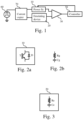
- Fig. 1 represents an example of the architecture of a device for sensing the temperature of a power semiconductor device according to the invention.
- the device for sensing the temperature of a power semiconductor comprises a current copier 70 that duplicates the current provided by a current pulse source 60 through control electrodes of a power semiconductor Sc 10 when the power semiconductor is not switching or in a transition mode.
- Control electrodes are a gate and an emitter or a gate and a source.
- the duplicated current is provided to an emulating device 20.
- the sensed voltage across the gate and the emitter or the gate and the source voltage of the power semiconductor 10 is provided to a comparator 30 that compares the voltage of the emulating device 20.
- the voltage is sensed across one control electrode and a reference, like for example, the ground.
- the output of the comparator 30 reaches high level.
- the device for sensing the temperature of a power semiconductor comprises a controller 50 that notifies the result of the comparison by transferring a predetermined signal or a predetermined message or generates a predetermined information through a man machine interface.
- the controller further controls the gate to source voltage of the power semiconductor and modifies the gate to source voltage patterns applied to the power semiconductor device during operation in order to reduce the junction temperature of the power semiconductor 10.
- the emulating device is an emulating impedance which is representative of the input impedance, like the one of the gate/emitter path, of the power semiconductor 10 at the desired temperature to be detected.
- the pulse duration of the pulse current source 60 is controlled to certain periods, typically several microseconds, to avoid switching-on or switching-off the power semiconductor. Then, the voltage across the real transistor is compared to the voltage across the emulating impedance. Thus, when the voltage measured is higher than the voltage at the emulating device, meaning that the gate resistance has a higher value than the emulating device one, the junction temperature of the power semi conductor 10 is hotter than the target point, the comparator 30 outputs a signal indicating the temperature overrun. Finally, the over temperature signal is fed to the controller 50 that notifies the result of the comparison.
- the controller 50 further reduces switching speed of power semiconductor or stops switching for a moment.
- the present invention permits to detect the over temperature during the normal operation of the power semiconductor, without any additional device near the power semiconductor, with a fast bandwidth, without any analogue to digital converter or need for digital processing.
- Fig. 2a represents an example of a power semiconductor.
- the power semiconductor is for example a transistor T and a diode D the anode of which is connected to the emitter of the transistor T and the cathode of which is connected to the collector of the transistor T.
- Fig. 2b represents the electric equivalent circuit of the power semiconductor according to the present invention.
- the electric equivalent circuit of the power semiconductor is composed of a resistor Rg connected in series with a capacitor Cg.
- the present invention utilises the internal gate resistance to infer the junction temperature.
- the internal gate resistance is created by the polysilicon layer in Field Effect Transistors which is already present in the classical structures of the transistor. In the case of typical transistors, the value of the resistance increases as the temperature increases.
- Fig. 3 represents an example of an emulating device that is used for sensing the temperature of a power semiconductor according to the present invention.
- the emulating device 20 is composed of a resistor Re connected in series with a capacitor Ce.
- the resistor Re has the same value as Rg at the maximum safe temperature operation and the capacitor Ce is for example a high-stability (such as C0G) capacitor with the same value as Cg.
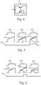
- Fig. 4 represents an example of a current copier that is used for sensing the temperature of a power semiconductor according to the present invention.
- the current copier 70 is for example composed of gain-matched transistor pairs.
- Fig. 5 represents signals that are used for sensing the temperature of a power semiconductor according to the present invention.
- the waveforms of the pulsed current 60, the voltages 10o of the power semiconductor 10 and the voltage of the emulating device 20 and the over-temperature signals 50o are shown in Fig. 5 for three pulses.
- the power semiconductor 10 temperature is equal to the maximum junction temperature.
- the power semiconductor 10 temperature is inferior to the maximum junction temperature.
- the voltage 10ob is upper than the voltage 20ob.
- the power semicondcutor temperature is superior to the temperature threshold i.e. the maximum junction temperature.
- the voltage 20oc is upper than the voltage 10oc and the output signal 50o of the comparator 30 changes of state.
- Fig. 6 represents signals that may occur when at least one component value of the emulating device is not accurately defined.
- the capacitor Ce is strictly smaller or equal to Cg, avoiding the generation of false alarms. As shown in Fig. 6 , this condition is necessary and sufficient to maintain the voltage 10o inferior to the voltage 20o at the end of the current pulse for a resistor value Rg inferior to the resistor value Re.
- the capacitor value Ce is equal to the capacitor value Cg, no false alarm is possible, even for infinite pulse duration.
- the capacitor value Ce is superior to the capacitor value Cg, then even for a resistor value Rg smaller than the resistor value Re, a false trigger is outputted.
- the capacitor value Ce is lower than the capacitor value Cg, no false alarm is possible, even for infinite pulse duration.
- Vsupply is the negative gate voltage that prevents the power semiconductor to turn-on or Vsupply is the positive gate voltage that prevents the power semiconductor to turn-off.
- the resistor Re is set to a slightly smaller or equal value of the resistor Rg at the maximum temperature.
- R g @ Tmax is the resistor value at maximum junction temperature.
- Fig. 7 represents signals that occur when the maximum junction temperature is detected.
- Fig. 8 represents an example of an algorithm that is used for adjusting the value of a resistor of the emulating power semiconductor.
- the power semiconductor is heated at a predetermined temperature, for example at the maximum junction temperature minus one degree.
- step S81 the over-temperature signal outputted by the comparator 30 is checked. If the signal is at high level, the algorithm moves to step S81. Otherwise, the present algorithm is interrupted.
- the resistor value Re value is adjusted using a laser trimming technique or fuse blowing.
- the resistor value Re is adjusted by an increment if the over-temperature signal outputted by the comparator is in high level.
- the increment is equal to 1000ppm of the estimated Rg resistor value, e.g. 5mQ for Rg with a nominal value of 5 ⁇ .
- Fig. 9 represents an example of the architecture of a device for sensing the temperature of a power semiconductor device according to the present invention.
- the device 60 has, for example, an architecture based on components connected together by a bus 901 and a processor 900 controlled by a program.
- the bus 901 links the processor 900 to a read only memory ROM 902, a random access memory RAM 903, and an input output I/O interface I/F 905.
- the input output interface I/F 905 comprises the current pulse source, the current copier 70, the emulating device 20 and the comparator 30.
- the memory 903 contains registers intended to receive variables and the instructions of the program related to the algorithm disclosed in Fig. 11 .
- the read-only memory or possibly a flash memory 902, contains instructions of the program related to the algorithm disclosed in Fig. 11 .
- the device may be implemented in software by execution of a set of instructions or program by a programmable computing machine, such as a PC ( Personal Computer ), a DSP ( Digital Signal Processor ) or a microcontroller; or else implemented in hardware by a machine or a dedicated component, such as an FPGA ( Field-Programmable Gate Array ) or an ASIC ( Application-Specific Integrated Circuit ).
- a programmable computing machine such as a PC ( Personal Computer ), a DSP ( Digital Signal Processor ) or a microcontroller; or else implemented in hardware by a machine or a dedicated component, such as an FPGA ( Field-Programmable Gate Array ) or an ASIC ( Application-Specific Integrated Circuit ).
- the device includes circuitry, enabling the controller 50 to perform the program.
- the device 60 controls the gate signal of the semiconductor through the input output I/O interface I/F 905, controls the switching of the power semi conductor and may control a laser triming device for adjusting the value of the resistor of the emulating device.
- Fig. 10 represents another example of the architecture of a device for sensing the temperature of a power semiconductor device according to the invention.
- the device for sensing the temperature of a power semiconductor 10 comprises a current copier 70 that duplicates the current provided by a current pulse source 60 through control electrodes of a power semiconductor Sc 10.
- the duplicated current is provided to a first terminal of a resistor R1 and to a first input of a comparator 31.
- a second terminal of the resistor R1 is connected to a first terminal of a resistor R2 and to a first input of a comparator 32.
- a second terminal of the resistor R2 is connected to the emulating device 20.
- the sensed voltage across the control electrodes of the power semiconductor 10 is provided to the comparators 31, 32 and 33 that compares the voltage of the emulating device 20.
- the output of the comparator 30 reaches high level.
- the device for sensing the temperature of a power semiconductor comprises a controller 50 that notifies the result of the comparison.
- the controller 50 modifies the patterns applied to the power semiconductor device during operation in order to reduce the junction temperature of the power semiconductor 10.
- the emulating device is an emulating impedance which is representative of the input impedance (gate/emitter path) of the power semiconductor 10 at the desired temperature to be detected.
- the resistor Re value is adjusted for a given temperature using one of the techniques described above.
- the resistor R1 and R2 values are chosen in function of the temperature sensitivity of the resistor Rg value multiplied by temperature steps. Taking the numerical example above, if the temperature steps are 5°C and the temperature sensitivity is 5m ⁇ /°C, thus the resistor R1 and R2 values are 25m ⁇ .
- the pulse duration of the pulse current source 60 is controlled to certain periods, typically several microseconds, to avoid switching-on or switching-off the power semiconductor. Then, the voltage across the electrode of the semiconductor is compared to the voltage across the emulating impedance.
- Fig. 11 represents an example of an algorithm for sensing the temperature of a power semiconductor device according to the invention.
- a current pulse is applied through control electrodes of the power semiconductor.
- the current pulse is duplicated, and the duplicated current pulse is provided to the emulating device.
- step S112 the voltage across the control electrodes of the power semiconductor is compared to the voltage at the emulating device.
- step S113 the result of the comparison is notified.
- the switching pattern of the power semiconductor may be also controlled according to the result of the comparison.
Landscapes
- Physics & Mathematics (AREA)
- General Physics & Mathematics (AREA)
- Engineering & Computer Science (AREA)
- Power Engineering (AREA)
- Power Conversion In General (AREA)
- Semiconductor Integrated Circuits (AREA)
- Measuring Temperature Or Quantity Of Heat (AREA)
- Testing Of Individual Semiconductor Devices (AREA)
Claims (9)
- Dispositif de détection d'une surchauffe d'un semi-conducteur de puissance, caractérisé en ce que le dispositif comprend :- une source d'impulsions de courant (60) fournie par le biais d'électrodes de commande du semi-conducteur de puissance,- un copieur de courant (70) qui duplique le courant fourni par la source d'impulsions de courant, et qui fournit le courant dupliqué à un dispositif d'émulation (20), le dispositif d'émulation étant composé d'une résistance Re et d'un condensateur Ce connectés en série, le circuit équivalent du semi-conducteur de puissance étant composé d'une résistance Rg connectée en série avec un condensateur de grille Cg, la valeur de la résistance Re est égale ou inférieure à une valeur de résistance de grille du semi-conducteur de puissance lorsque le semi-conducteur de puissance est à une température presque égale à la température maximale de jonction du semi-conducteur de puissance et la valeur du condensateur Ce est égale ou inférieure à la valeur de capacité de grille Cg du semi-conducteur de puissance,- un comparateur (30) qui compare la tension aux bornes des électrodes de commande à la tension aux bornes du dispositif d'émulation,- un moyen de notification du résultat de la comparaison.
- Dispositif selon la revendication l, caractérisé en ce que le moyen de notification du résultat de la comparaison commande en outre le schéma de commutation du semi-conducteur de puissance en fonction du signal délivré par le comparateur.
- Dispositif selon la revendication 1 ou 2, caractérisé en ce que les électrodes de commande auxquelles la source de courant est appliquée sont une grille et un émetteur ou une grille et une source.
- Dispositif selon la revendication 2, dans lequel la source d'impulsions de courant est fournie au semi-conducteur de puissance lorsque le semi-conducteur de puissance ne commute pas ou n'est pas en mode de transition.
- Dispositif selon la revendication l, caractérisé en ce que la valeur de la résistance est ajustée durant une phase d'étalonnage.
- Dispositif selon la revendication 5, caractérisé en ce que la durée des impulsions de courant est égale à :

- Dispositif selon l'une quelconque des revendications 1 à 6, caractérisé en ce que le dispositif comprend en outre au moins une résistance et au moins un autre comparateur, une première borne de l'au moins une résistance est connectée au copieur de courant et une seconde borne de l'au moins une résistance est connectée au dispositif d'émulation et l'au moins un autre comparateur compare la tension au niveau de l'électrode du semi-conducteur de puissance à la tension au niveau de la seconde borne de l'au moins une résistance.
- Procédé de détection d'une surchauffe d'un semi-conducteur de puissance, caractérisé en ce que le procédé comprend les étapes suivantes :- l'application d'une impulsion de courant à travers des électrodes de commande du semi-conducteur de puissance,- la duplication de l'impulsion de courant et la fourniture de l'impulsion de courant dupliquée à un dispositif d'émulation, le dispositif d'émulation étant composé d'une résistance Re et d'un condensateur Ce connectés en série, le circuit équivalent du semi-conducteur de puissance étant composé d'une résistance Rg connectée en série avec un condensateur de grille Cg, la valeur de la résistance Re de la résistance est égale ou inférieure à une valeur de résistance de grille du semi-conducteur de puissance lorsque le semi-conducteur de puissance est à une température presque égale à la température maximale de jonction du semi-conducteur de puissance et la valeur du condensateur Ce est égale ou inférieure à la valeur de capacité de grille Cg du semi-conducteur de puissance,- la comparaison de la tension aux bornes des électrodes de commande à la tension aux bornes du dispositif d'émulation,- la notification du résultat de la comparaison.
- Procédé selon la revendication 8, caractérisé en ce que le procédé comprend en outre l'étape d'ajustement de la valeur de la résistance lorsque le semi-conducteur de puissance est chauffé à une température prédéterminée.
Priority Applications (5)
| Application Number | Priority Date | Filing Date | Title |
|---|---|---|---|
| EP20152878.3A EP3855145B1 (fr) | 2020-01-21 | 2020-01-21 | Dispositif pour la détection d'une surchauffe d'un dispositif de puissance à semiconducteur |
| PCT/JP2020/048325 WO2021149451A1 (fr) | 2020-01-21 | 2020-12-17 | Dispositif et procédé de détection d'une surchauffe d'un semi-conducteur de puissance |
| US17/789,721 US12416528B2 (en) | 2020-01-21 | 2020-12-17 | Device and method for sensing an over-temperature of a power semiconductor |
| JP2022553429A JP7361941B2 (ja) | 2020-01-21 | 2020-12-17 | パワー半導体の温度過昇を検知する装置及び方法 |
| CN202080092903.0A CN114930137B (zh) | 2020-01-21 | 2020-12-17 | 用于感测功率半导体的过温的装置和方法 |
Applications Claiming Priority (1)
| Application Number | Priority Date | Filing Date | Title |
|---|---|---|---|
| EP20152878.3A EP3855145B1 (fr) | 2020-01-21 | 2020-01-21 | Dispositif pour la détection d'une surchauffe d'un dispositif de puissance à semiconducteur |
Publications (2)
| Publication Number | Publication Date |
|---|---|
| EP3855145A1 EP3855145A1 (fr) | 2021-07-28 |
| EP3855145B1 true EP3855145B1 (fr) | 2023-06-14 |
Family
ID=69185509
Family Applications (1)
| Application Number | Title | Priority Date | Filing Date |
|---|---|---|---|
| EP20152878.3A Active EP3855145B1 (fr) | 2020-01-21 | 2020-01-21 | Dispositif pour la détection d'une surchauffe d'un dispositif de puissance à semiconducteur |
Country Status (5)
| Country | Link |
|---|---|
| US (1) | US12416528B2 (fr) |
| EP (1) | EP3855145B1 (fr) |
| JP (1) | JP7361941B2 (fr) |
| CN (1) | CN114930137B (fr) |
| WO (1) | WO2021149451A1 (fr) |
Families Citing this family (2)
| Publication number | Priority date | Publication date | Assignee | Title |
|---|---|---|---|---|
| EP4439026B1 (fr) | 2023-03-29 | 2025-04-02 | Mitsubishi Electric R&D Centre Europe B.V. | Résolution dynamique en ligne d'estimation de température basée sur le temps |
| EP4439025B1 (fr) * | 2023-03-29 | 2025-04-02 | Mitsubishi Electric R&D Centre Europe Bv | Estimation et étalonnage de température de jonction basée sur le temps à haute résolution |
Citations (1)
| Publication number | Priority date | Publication date | Assignee | Title |
|---|---|---|---|---|
| EP0360333B1 (fr) * | 1988-09-19 | 1995-12-27 | Philips Electronics Uk Limited | Montage pour capter un seuil de température |
Family Cites Families (19)
| Publication number | Priority date | Publication date | Assignee | Title |
|---|---|---|---|---|
| CA1010574A (en) * | 1974-12-02 | 1977-05-17 | Canadian General Electric Company Limited | Temperature monitoring of semiconductors |
| JP3135245B2 (ja) * | 1990-03-19 | 2001-02-13 | 株式会社日立製作所 | パルス出力型熱線式空気流量計 |
| US6092927A (en) * | 1994-11-10 | 2000-07-25 | International Rectifier Corp. | Temperature detection of power semiconductors performed by a co-packaged analog integrated circuit |
| US6055489A (en) * | 1997-04-15 | 2000-04-25 | Intel Corporation | Temperature measurement and compensation scheme |
| JP3225887B2 (ja) * | 1997-05-16 | 2001-11-05 | 日本電気株式会社 | 半導体集積回路装置 |
| US6998899B2 (en) * | 2003-05-12 | 2006-02-14 | Nadd Bruno C | Method and apparatus to remotely sense the temperature of a power semiconductor |
| FR2857456B1 (fr) | 2003-07-07 | 2006-01-13 | St Microelectronics Sa | Cellule de detection de temperature et procede de determination du seuil de detection d'une telle cellule |
| DE102006005033B4 (de) * | 2006-02-03 | 2013-12-05 | Infineon Technologies Ag | Halbleiterbauelementanordnung mit einem Leistungstransistor und einer Temperaturmessanordnung |
| US7906860B2 (en) * | 2007-10-26 | 2011-03-15 | Infineon Technologies Ag | Semiconductor device |
| US7988354B2 (en) * | 2007-12-26 | 2011-08-02 | Infineon Technologies Ag | Temperature detection for a semiconductor component |
| DE102010000875B4 (de) * | 2010-01-13 | 2014-05-22 | Infineon Technologies Ag | Verfahren zur Messung der Junction-Temperatur bei Leistungshalbleitern in einem Stromrichter |
| KR101293280B1 (ko) * | 2011-07-15 | 2013-08-09 | 주식회사 오토닉스 | 멀티입력회로 |
| DK177863B1 (en) * | 2013-03-27 | 2014-10-13 | Electronic As Kk | Intelligent gate drive unit |
| CN104634466B (zh) * | 2013-11-14 | 2018-07-06 | 北京华峰测控技术有限公司 | 半导体功率器件结温仿真电路 |
| JP6953512B2 (ja) * | 2016-08-08 | 2021-10-27 | パワー・インテグレーションズ・インコーポレーテッド | 半導体スイッチングデバイスの高速温度検出のための集積回路 |
| US10348487B2 (en) * | 2017-07-20 | 2019-07-09 | International Business Machines Corporation | Game data offloading to a blockchain |
| US20190028065A1 (en) * | 2017-07-24 | 2019-01-24 | Macom Technology Solutions Holdings, Inc. | Fet operational temperature determination by gate structure resistance thermometry |
| KR102338628B1 (ko) * | 2017-12-29 | 2021-12-10 | 에스케이하이닉스 주식회사 | 온도 센서 회로 및 이를 구비하는 반도체 장치 |
| CN208727642U (zh) * | 2018-04-28 | 2019-04-12 | 吴乐建 | 一种球磨机衬板 |
-
2020
- 2020-01-21 EP EP20152878.3A patent/EP3855145B1/fr active Active
- 2020-12-17 CN CN202080092903.0A patent/CN114930137B/zh active Active
- 2020-12-17 JP JP2022553429A patent/JP7361941B2/ja active Active
- 2020-12-17 WO PCT/JP2020/048325 patent/WO2021149451A1/fr not_active Ceased
- 2020-12-17 US US17/789,721 patent/US12416528B2/en active Active
Patent Citations (1)
| Publication number | Priority date | Publication date | Assignee | Title |
|---|---|---|---|---|
| EP0360333B1 (fr) * | 1988-09-19 | 1995-12-27 | Philips Electronics Uk Limited | Montage pour capter un seuil de température |
Also Published As
| Publication number | Publication date |
|---|---|
| JP7361941B2 (ja) | 2023-10-16 |
| CN114930137B (zh) | 2026-04-24 |
| US12416528B2 (en) | 2025-09-16 |
| US20230053137A1 (en) | 2023-02-16 |
| EP3855145A1 (fr) | 2021-07-28 |
| JP2023500981A (ja) | 2023-01-11 |
| WO2021149451A1 (fr) | 2021-07-29 |
| CN114930137A (zh) | 2022-08-19 |
Similar Documents
| Publication | Publication Date | Title |
|---|---|---|
| CN108770363B (zh) | 用于确定半导体功率模块的芯片的结的温度的方法和装置 | |
| US10036771B2 (en) | Circuit arrangement | |
| US12416528B2 (en) | Device and method for sensing an over-temperature of a power semiconductor | |
| US20100321846A1 (en) | Semiconductor apparatus and temperature detection circuit | |
| CN110431430B (zh) | 用于控制多芯片功率模块的健康的方法和多芯片健康监测装置 | |
| US7332358B2 (en) | MOSFET temperature sensing | |
| CN113741673B (zh) | 一种应用于热插拔服务器的保护装置 | |
| US20180309436A1 (en) | Control device for a power semiconductor switch | |
| US11388845B2 (en) | Multi-die temperature control device and method for controlling temperature of multi-die power module | |
| CN120490762B (zh) | 一种导通压降测量电路、结温监测方法及功率变流器 | |
| CN117092473A (zh) | 一种功率器件的状态监测方法及装置 | |
| US7121721B2 (en) | Apparatus and method for measuring operating temperatures of an electrical component | |
| US12480823B2 (en) | Method and system for determining junction temperature of power semiconductor | |
| JP7132197B2 (ja) | 保護回路、半導体装置及び方法 | |
| CN114625198A (zh) | 过温保护阈值测量装置及其测量方法 | |
| CN119542910A (zh) | 半导体激光器脉冲式驱动电路及其驱动电流检测、控制方法 | |
| US20250155294A1 (en) | Measurement method for estimating temperature of power semiconductor module | |
| CN116593022A (zh) | 温度感测装置 | |
| JPH05241671A (ja) | 基準電圧発生装置および過電流防止機能付半導体装置 | |
| US9000830B2 (en) | Method and apparatus for protecting transistors | |
| Lu et al. | A Novel Method for Turn-Off Delay Detection in SiC MOSFETs with Application to Online Junction Temperature Monitoring | |
| US20260106445A1 (en) | Electronic fuse device | |
| EP0039460A2 (fr) | Thermomètre médical électronique | |
| CN119959717A (zh) | 一种智能功率模块的过温检测电路和智能功率模块 | |
| CN121749961A (zh) | 保护电路、对应的系统和方法 |
Legal Events
| Date | Code | Title | Description |
|---|---|---|---|
| PUAI | Public reference made under article 153(3) epc to a published international application that has entered the european phase |
Free format text: ORIGINAL CODE: 0009012 |
|
| STAA | Information on the status of an ep patent application or granted ep patent |
Free format text: STATUS: THE APPLICATION HAS BEEN PUBLISHED |
|
| AK | Designated contracting states |
Kind code of ref document: A1 Designated state(s): AL AT BE BG CH CY CZ DE DK EE ES FI FR GB GR HR HU IE IS IT LI LT LU LV MC MK MT NL NO PL PT RO RS SE SI SK SM TR |
|
| STAA | Information on the status of an ep patent application or granted ep patent |
Free format text: STATUS: REQUEST FOR EXAMINATION WAS MADE |
|
| 17P | Request for examination filed |
Effective date: 20220127 |
|
| RBV | Designated contracting states (corrected) |
Designated state(s): AL AT BE BG CH CY CZ DE DK EE ES FI FR GB GR HR HU IE IS IT LI LT LU LV MC MK MT NL NO PL PT RO RS SE SI SK SM TR |
|
| GRAP | Despatch of communication of intention to grant a patent |
Free format text: ORIGINAL CODE: EPIDOSNIGR1 |
|
| STAA | Information on the status of an ep patent application or granted ep patent |
Free format text: STATUS: GRANT OF PATENT IS INTENDED |
|
| RIC1 | Information provided on ipc code assigned before grant |
Ipc: G01K 7/01 20060101ALI20230207BHEP Ipc: G01K 3/00 20060101AFI20230207BHEP |
|
| INTG | Intention to grant announced |
Effective date: 20230224 |
|
| RIN1 | Information on inventor provided before grant (corrected) |
Inventor name: MOLLOV, M. STEFAN Inventor name: BRANDELERO, M. JULIO Inventor name: KAWAHARA, M. CHIHIRO |
|
| GRAS | Grant fee paid |
Free format text: ORIGINAL CODE: EPIDOSNIGR3 |
|
| GRAA | (expected) grant |
Free format text: ORIGINAL CODE: 0009210 |
|
| STAA | Information on the status of an ep patent application or granted ep patent |
Free format text: STATUS: THE PATENT HAS BEEN GRANTED |
|
| AK | Designated contracting states |
Kind code of ref document: B1 Designated state(s): AL AT BE BG CH CY CZ DE DK EE ES FI FR GB GR HR HU IE IS IT LI LT LU LV MC MK MT NL NO PL PT RO RS SE SI SK SM TR |
|
| REG | Reference to a national code |
Ref country code: CH Ref legal event code: EP |
|
| P01 | Opt-out of the competence of the unified patent court (upc) registered |
Effective date: 20230524 |
|
| REG | Reference to a national code |
Ref country code: DE Ref legal event code: R096 Ref document number: 602020012393 Country of ref document: DE |
|
| REG | Reference to a national code |
Ref country code: AT Ref legal event code: REF Ref document number: 1579558 Country of ref document: AT Kind code of ref document: T Effective date: 20230715 |
|
| REG | Reference to a national code |
Ref country code: LT Ref legal event code: MG9D |
|
| REG | Reference to a national code |
Ref country code: NL Ref legal event code: MP Effective date: 20230614 |
|
| PG25 | Lapsed in a contracting state [announced via postgrant information from national office to epo] |
Ref country code: SE Free format text: LAPSE BECAUSE OF FAILURE TO SUBMIT A TRANSLATION OF THE DESCRIPTION OR TO PAY THE FEE WITHIN THE PRESCRIBED TIME-LIMIT Effective date: 20230614 Ref country code: NO Free format text: LAPSE BECAUSE OF FAILURE TO SUBMIT A TRANSLATION OF THE DESCRIPTION OR TO PAY THE FEE WITHIN THE PRESCRIBED TIME-LIMIT Effective date: 20230914 Ref country code: ES Free format text: LAPSE BECAUSE OF FAILURE TO SUBMIT A TRANSLATION OF THE DESCRIPTION OR TO PAY THE FEE WITHIN THE PRESCRIBED TIME-LIMIT Effective date: 20230614 |
|
| REG | Reference to a national code |
Ref country code: AT Ref legal event code: MK05 Ref document number: 1579558 Country of ref document: AT Kind code of ref document: T Effective date: 20230614 |
|
| PG25 | Lapsed in a contracting state [announced via postgrant information from national office to epo] |
Ref country code: RS Free format text: LAPSE BECAUSE OF FAILURE TO SUBMIT A TRANSLATION OF THE DESCRIPTION OR TO PAY THE FEE WITHIN THE PRESCRIBED TIME-LIMIT Effective date: 20230614 Ref country code: NL Free format text: LAPSE BECAUSE OF FAILURE TO SUBMIT A TRANSLATION OF THE DESCRIPTION OR TO PAY THE FEE WITHIN THE PRESCRIBED TIME-LIMIT Effective date: 20230614 Ref country code: LV Free format text: LAPSE BECAUSE OF FAILURE TO SUBMIT A TRANSLATION OF THE DESCRIPTION OR TO PAY THE FEE WITHIN THE PRESCRIBED TIME-LIMIT Effective date: 20230614 Ref country code: LT Free format text: LAPSE BECAUSE OF FAILURE TO SUBMIT A TRANSLATION OF THE DESCRIPTION OR TO PAY THE FEE WITHIN THE PRESCRIBED TIME-LIMIT Effective date: 20230614 Ref country code: HR Free format text: LAPSE BECAUSE OF FAILURE TO SUBMIT A TRANSLATION OF THE DESCRIPTION OR TO PAY THE FEE WITHIN THE PRESCRIBED TIME-LIMIT Effective date: 20230614 Ref country code: GR Free format text: LAPSE BECAUSE OF FAILURE TO SUBMIT A TRANSLATION OF THE DESCRIPTION OR TO PAY THE FEE WITHIN THE PRESCRIBED TIME-LIMIT Effective date: 20230915 |
|
| PG25 | Lapsed in a contracting state [announced via postgrant information from national office to epo] |
Ref country code: FI Free format text: LAPSE BECAUSE OF FAILURE TO SUBMIT A TRANSLATION OF THE DESCRIPTION OR TO PAY THE FEE WITHIN THE PRESCRIBED TIME-LIMIT Effective date: 20230614 |
|
| PG25 | Lapsed in a contracting state [announced via postgrant information from national office to epo] |
Ref country code: SK Free format text: LAPSE BECAUSE OF FAILURE TO SUBMIT A TRANSLATION OF THE DESCRIPTION OR TO PAY THE FEE WITHIN THE PRESCRIBED TIME-LIMIT Effective date: 20230614 |
|
| REG | Reference to a national code |
Ref country code: DE Ref legal event code: R082 Ref document number: 602020012393 Country of ref document: DE Representative=s name: PUSCHMANN BORCHERT KAISER KLETTNER PATENTANWAE, DE Ref country code: DE Ref legal event code: R082 Ref document number: 602020012393 Country of ref document: DE Representative=s name: PATCARE PATENTANWAELTE PARTNERSCHAFT MBB, DE |
|
| PG25 | Lapsed in a contracting state [announced via postgrant information from national office to epo] |
Ref country code: IS Free format text: LAPSE BECAUSE OF FAILURE TO SUBMIT A TRANSLATION OF THE DESCRIPTION OR TO PAY THE FEE WITHIN THE PRESCRIBED TIME-LIMIT Effective date: 20231014 |
|
| PG25 | Lapsed in a contracting state [announced via postgrant information from national office to epo] |
Ref country code: SM Free format text: LAPSE BECAUSE OF FAILURE TO SUBMIT A TRANSLATION OF THE DESCRIPTION OR TO PAY THE FEE WITHIN THE PRESCRIBED TIME-LIMIT Effective date: 20230614 Ref country code: SK Free format text: LAPSE BECAUSE OF FAILURE TO SUBMIT A TRANSLATION OF THE DESCRIPTION OR TO PAY THE FEE WITHIN THE PRESCRIBED TIME-LIMIT Effective date: 20230614 Ref country code: RO Free format text: LAPSE BECAUSE OF FAILURE TO SUBMIT A TRANSLATION OF THE DESCRIPTION OR TO PAY THE FEE WITHIN THE PRESCRIBED TIME-LIMIT Effective date: 20230614 Ref country code: PT Free format text: LAPSE BECAUSE OF FAILURE TO SUBMIT A TRANSLATION OF THE DESCRIPTION OR TO PAY THE FEE WITHIN THE PRESCRIBED TIME-LIMIT Effective date: 20231016 Ref country code: IS Free format text: LAPSE BECAUSE OF FAILURE TO SUBMIT A TRANSLATION OF THE DESCRIPTION OR TO PAY THE FEE WITHIN THE PRESCRIBED TIME-LIMIT Effective date: 20231014 Ref country code: EE Free format text: LAPSE BECAUSE OF FAILURE TO SUBMIT A TRANSLATION OF THE DESCRIPTION OR TO PAY THE FEE WITHIN THE PRESCRIBED TIME-LIMIT Effective date: 20230614 Ref country code: CZ Free format text: LAPSE BECAUSE OF FAILURE TO SUBMIT A TRANSLATION OF THE DESCRIPTION OR TO PAY THE FEE WITHIN THE PRESCRIBED TIME-LIMIT Effective date: 20230614 Ref country code: AT Free format text: LAPSE BECAUSE OF FAILURE TO SUBMIT A TRANSLATION OF THE DESCRIPTION OR TO PAY THE FEE WITHIN THE PRESCRIBED TIME-LIMIT Effective date: 20230614 |
|
| PG25 | Lapsed in a contracting state [announced via postgrant information from national office to epo] |
Ref country code: PL Free format text: LAPSE BECAUSE OF FAILURE TO SUBMIT A TRANSLATION OF THE DESCRIPTION OR TO PAY THE FEE WITHIN THE PRESCRIBED TIME-LIMIT Effective date: 20230614 |
|
| REG | Reference to a national code |
Ref country code: DE Ref legal event code: R097 Ref document number: 602020012393 Country of ref document: DE |
|
| PLBE | No opposition filed within time limit |
Free format text: ORIGINAL CODE: 0009261 |
|
| STAA | Information on the status of an ep patent application or granted ep patent |
Free format text: STATUS: NO OPPOSITION FILED WITHIN TIME LIMIT |
|
| PG25 | Lapsed in a contracting state [announced via postgrant information from national office to epo] |
Ref country code: DK Free format text: LAPSE BECAUSE OF FAILURE TO SUBMIT A TRANSLATION OF THE DESCRIPTION OR TO PAY THE FEE WITHIN THE PRESCRIBED TIME-LIMIT Effective date: 20230614 |
|
| PG25 | Lapsed in a contracting state [announced via postgrant information from national office to epo] |
Ref country code: SI Free format text: LAPSE BECAUSE OF FAILURE TO SUBMIT A TRANSLATION OF THE DESCRIPTION OR TO PAY THE FEE WITHIN THE PRESCRIBED TIME-LIMIT Effective date: 20230614 |
|
| 26N | No opposition filed |
Effective date: 20240315 |
|
| PG25 | Lapsed in a contracting state [announced via postgrant information from national office to epo] |
Ref country code: SI Free format text: LAPSE BECAUSE OF FAILURE TO SUBMIT A TRANSLATION OF THE DESCRIPTION OR TO PAY THE FEE WITHIN THE PRESCRIBED TIME-LIMIT Effective date: 20230614 Ref country code: IT Free format text: LAPSE BECAUSE OF FAILURE TO SUBMIT A TRANSLATION OF THE DESCRIPTION OR TO PAY THE FEE WITHIN THE PRESCRIBED TIME-LIMIT Effective date: 20230614 |
|
| PG25 | Lapsed in a contracting state [announced via postgrant information from national office to epo] |
Ref country code: MC Free format text: LAPSE BECAUSE OF FAILURE TO SUBMIT A TRANSLATION OF THE DESCRIPTION OR TO PAY THE FEE WITHIN THE PRESCRIBED TIME-LIMIT Effective date: 20230614 |
|
| PG25 | Lapsed in a contracting state [announced via postgrant information from national office to epo] |
Ref country code: MC Free format text: LAPSE BECAUSE OF FAILURE TO SUBMIT A TRANSLATION OF THE DESCRIPTION OR TO PAY THE FEE WITHIN THE PRESCRIBED TIME-LIMIT Effective date: 20230614 |
|
| REG | Reference to a national code |
Ref country code: CH Ref legal event code: PL |
|
| PG25 | Lapsed in a contracting state [announced via postgrant information from national office to epo] |
Ref country code: LU Free format text: LAPSE BECAUSE OF NON-PAYMENT OF DUE FEES Effective date: 20240121 |
|
| PG25 | Lapsed in a contracting state [announced via postgrant information from national office to epo] |
Ref country code: LU Free format text: LAPSE BECAUSE OF NON-PAYMENT OF DUE FEES Effective date: 20240121 |
|
| PG25 | Lapsed in a contracting state [announced via postgrant information from national office to epo] |
Ref country code: BE Free format text: LAPSE BECAUSE OF NON-PAYMENT OF DUE FEES Effective date: 20240131 |
|
| PG25 | Lapsed in a contracting state [announced via postgrant information from national office to epo] |
Ref country code: CH Free format text: LAPSE BECAUSE OF NON-PAYMENT OF DUE FEES Effective date: 20240131 |
|
| PG25 | Lapsed in a contracting state [announced via postgrant information from national office to epo] |
Ref country code: CH Free format text: LAPSE BECAUSE OF NON-PAYMENT OF DUE FEES Effective date: 20240131 Ref country code: BE Free format text: LAPSE BECAUSE OF NON-PAYMENT OF DUE FEES Effective date: 20240131 |
|
| REG | Reference to a national code |
Ref country code: BE Ref legal event code: MM Effective date: 20240131 |
|
| PG25 | Lapsed in a contracting state [announced via postgrant information from national office to epo] |
Ref country code: BG Free format text: LAPSE BECAUSE OF FAILURE TO SUBMIT A TRANSLATION OF THE DESCRIPTION OR TO PAY THE FEE WITHIN THE PRESCRIBED TIME-LIMIT Effective date: 20230614 |
|
| PG25 | Lapsed in a contracting state [announced via postgrant information from national office to epo] |
Ref country code: BG Free format text: LAPSE BECAUSE OF FAILURE TO SUBMIT A TRANSLATION OF THE DESCRIPTION OR TO PAY THE FEE WITHIN THE PRESCRIBED TIME-LIMIT Effective date: 20230614 |
|
| PG25 | Lapsed in a contracting state [announced via postgrant information from national office to epo] |
Ref country code: IE Free format text: LAPSE BECAUSE OF NON-PAYMENT OF DUE FEES Effective date: 20240121 |
|
| PG25 | Lapsed in a contracting state [announced via postgrant information from national office to epo] |
Ref country code: IE Free format text: LAPSE BECAUSE OF NON-PAYMENT OF DUE FEES Effective date: 20240121 |
|
| PG25 | Lapsed in a contracting state [announced via postgrant information from national office to epo] |
Ref country code: CY Free format text: LAPSE BECAUSE OF FAILURE TO SUBMIT A TRANSLATION OF THE DESCRIPTION OR TO PAY THE FEE WITHIN THE PRESCRIBED TIME-LIMIT; INVALID AB INITIO Effective date: 20200121 |
|
| PG25 | Lapsed in a contracting state [announced via postgrant information from national office to epo] |
Ref country code: HU Free format text: LAPSE BECAUSE OF FAILURE TO SUBMIT A TRANSLATION OF THE DESCRIPTION OR TO PAY THE FEE WITHIN THE PRESCRIBED TIME-LIMIT; INVALID AB INITIO Effective date: 20200121 |
|
| PG25 | Lapsed in a contracting state [announced via postgrant information from national office to epo] |
Ref country code: TR Free format text: LAPSE BECAUSE OF FAILURE TO SUBMIT A TRANSLATION OF THE DESCRIPTION OR TO PAY THE FEE WITHIN THE PRESCRIBED TIME-LIMIT Effective date: 20230614 |
|
| PGFP | Annual fee paid to national office [announced via postgrant information from national office to epo] |
Ref country code: GB Payment date: 20251127 Year of fee payment: 7 |
|
| PGFP | Annual fee paid to national office [announced via postgrant information from national office to epo] |
Ref country code: FR Payment date: 20251128 Year of fee payment: 7 |
|
| PGFP | Annual fee paid to national office [announced via postgrant information from national office to epo] |
Ref country code: DE Payment date: 20251203 Year of fee payment: 7 |