EP3857592B1 - Agencement de fabrication de puces à modules multiples - Google Patents
Agencement de fabrication de puces à modules multiples Download PDFInfo
- Publication number
- EP3857592B1 EP3857592B1 EP19865166.3A EP19865166A EP3857592B1 EP 3857592 B1 EP3857592 B1 EP 3857592B1 EP 19865166 A EP19865166 A EP 19865166A EP 3857592 B1 EP3857592 B1 EP 3857592B1
- Authority
- EP
- European Patent Office
- Prior art keywords
- wafer
- solder balls
- arrangement
- binder
- module
- Prior art date
- Legal status (The legal status is an assumption and is not a legal conclusion. Google has not performed a legal analysis and makes no representation as to the accuracy of the status listed.)
- Active
Links
Images


Classifications
-
- H—ELECTRICITY
- H10—SEMICONDUCTOR DEVICES; ELECTRIC SOLID-STATE DEVICES NOT OTHERWISE PROVIDED FOR
- H10P—GENERIC PROCESSES OR APPARATUS FOR THE MANUFACTURE OR TREATMENT OF DEVICES COVERED BY CLASS H10
- H10P72/00—Handling or holding of wafers, substrates or devices during manufacture or treatment thereof
- H10P72/04—Apparatus for manufacture or treatment
- H10P72/0451—Apparatus for manufacturing or treating in a plurality of work-stations
- H10P72/0468—Apparatus for manufacturing or treating in a plurality of work-stations comprising a chamber adapted to a particular process
-
- B—PERFORMING OPERATIONS; TRANSPORTING
- B23—MACHINE TOOLS; METAL-WORKING NOT OTHERWISE PROVIDED FOR
- B23K—SOLDERING OR UNSOLDERING; WELDING; CLADDING OR PLATING BY SOLDERING OR WELDING; CUTTING BY APPLYING HEAT LOCALLY, e.g. FLAME CUTTING; WORKING BY LASER BEAM
- B23K1/00—Soldering, e.g. brazing, or unsoldering
- B23K1/0008—Soldering, e.g. brazing, or unsoldering specially adapted for particular articles or work
-
- B—PERFORMING OPERATIONS; TRANSPORTING
- B23—MACHINE TOOLS; METAL-WORKING NOT OTHERWISE PROVIDED FOR
- B23K—SOLDERING OR UNSOLDERING; WELDING; CLADDING OR PLATING BY SOLDERING OR WELDING; CUTTING BY APPLYING HEAT LOCALLY, e.g. FLAME CUTTING; WORKING BY LASER BEAM
- B23K1/00—Soldering, e.g. brazing, or unsoldering
- B23K1/008—Soldering within a furnace
-
- B—PERFORMING OPERATIONS; TRANSPORTING
- B23—MACHINE TOOLS; METAL-WORKING NOT OTHERWISE PROVIDED FOR
- B23K—SOLDERING OR UNSOLDERING; WELDING; CLADDING OR PLATING BY SOLDERING OR WELDING; CUTTING BY APPLYING HEAT LOCALLY, e.g. FLAME CUTTING; WORKING BY LASER BEAM
- B23K1/00—Soldering, e.g. brazing, or unsoldering
- B23K1/20—Preliminary treatment of work or areas to be soldered, e.g. in respect of a galvanic coating
- B23K1/203—Fluxing, i.e. applying flux onto surfaces
-
- B—PERFORMING OPERATIONS; TRANSPORTING
- B23—MACHINE TOOLS; METAL-WORKING NOT OTHERWISE PROVIDED FOR
- B23K—SOLDERING OR UNSOLDERING; WELDING; CLADDING OR PLATING BY SOLDERING OR WELDING; CUTTING BY APPLYING HEAT LOCALLY, e.g. FLAME CUTTING; WORKING BY LASER BEAM
- B23K3/00—Tools, devices or special appurtenances for soldering, e.g. brazing, or unsoldering, not specially adapted for particular methods
- B23K3/06—Solder feeding devices; Solder melting pans
- B23K3/0607—Solder feeding devices
- B23K3/0623—Solder feeding devices for shaped solder piece feeding, e.g. preforms, bumps, balls, pellets, droplets
-
- B—PERFORMING OPERATIONS; TRANSPORTING
- B23—MACHINE TOOLS; METAL-WORKING NOT OTHERWISE PROVIDED FOR
- B23K—SOLDERING OR UNSOLDERING; WELDING; CLADDING OR PLATING BY SOLDERING OR WELDING; CUTTING BY APPLYING HEAT LOCALLY, e.g. FLAME CUTTING; WORKING BY LASER BEAM
- B23K3/00—Tools, devices or special appurtenances for soldering, e.g. brazing, or unsoldering, not specially adapted for particular methods
- B23K3/08—Auxiliary devices therefor
- B23K3/082—Flux dispensers; Apparatus for applying flux
-
- H—ELECTRICITY
- H10—SEMICONDUCTOR DEVICES; ELECTRIC SOLID-STATE DEVICES NOT OTHERWISE PROVIDED FOR
- H10P—GENERIC PROCESSES OR APPARATUS FOR THE MANUFACTURE OR TREATMENT OF DEVICES COVERED BY CLASS H10
- H10P72/00—Handling or holding of wafers, substrates or devices during manufacture or treatment thereof
- H10P72/04—Apparatus for manufacture or treatment
- H10P72/0431—Apparatus for thermal treatment
- H10P72/0432—Apparatus for thermal treatment mainly by conduction
-
- H—ELECTRICITY
- H10—SEMICONDUCTOR DEVICES; ELECTRIC SOLID-STATE DEVICES NOT OTHERWISE PROVIDED FOR
- H10P—GENERIC PROCESSES OR APPARATUS FOR THE MANUFACTURE OR TREATMENT OF DEVICES COVERED BY CLASS H10
- H10P72/00—Handling or holding of wafers, substrates or devices during manufacture or treatment thereof
- H10P72/04—Apparatus for manufacture or treatment
- H10P72/0448—Apparatus for applying a liquid, a resin, an ink or the like
-
- H—ELECTRICITY
- H10—SEMICONDUCTOR DEVICES; ELECTRIC SOLID-STATE DEVICES NOT OTHERWISE PROVIDED FOR
- H10P—GENERIC PROCESSES OR APPARATUS FOR THE MANUFACTURE OR TREATMENT OF DEVICES COVERED BY CLASS H10
- H10P72/00—Handling or holding of wafers, substrates or devices during manufacture or treatment thereof
- H10P72/04—Apparatus for manufacture or treatment
- H10P72/0451—Apparatus for manufacturing or treating in a plurality of work-stations
- H10P72/0462—Apparatus for manufacturing or treating in a plurality of work-stations characterised by the construction of the processing chambers, e.g. modular processing chambers
-
- H—ELECTRICITY
- H10—SEMICONDUCTOR DEVICES; ELECTRIC SOLID-STATE DEVICES NOT OTHERWISE PROVIDED FOR
- H10P—GENERIC PROCESSES OR APPARATUS FOR THE MANUFACTURE OR TREATMENT OF DEVICES COVERED BY CLASS H10
- H10P72/00—Handling or holding of wafers, substrates or devices during manufacture or treatment thereof
- H10P72/06—Apparatus for monitoring, sorting, marking, testing or measuring
- H10P72/0602—Temperature monitoring
-
- H—ELECTRICITY
- H10—SEMICONDUCTOR DEVICES; ELECTRIC SOLID-STATE DEVICES NOT OTHERWISE PROVIDED FOR
- H10P—GENERIC PROCESSES OR APPARATUS FOR THE MANUFACTURE OR TREATMENT OF DEVICES COVERED BY CLASS H10
- H10P72/00—Handling or holding of wafers, substrates or devices during manufacture or treatment thereof
- H10P72/50—Handling or holding of wafers, substrates or devices during manufacture or treatment thereof for positioning, orientation or alignment
- H10P72/53—Handling or holding of wafers, substrates or devices during manufacture or treatment thereof for positioning, orientation or alignment using optical controlling means
-
- H—ELECTRICITY
- H10—SEMICONDUCTOR DEVICES; ELECTRIC SOLID-STATE DEVICES NOT OTHERWISE PROVIDED FOR
- H10P—GENERIC PROCESSES OR APPARATUS FOR THE MANUFACTURE OR TREATMENT OF DEVICES COVERED BY CLASS H10
- H10P72/00—Handling or holding of wafers, substrates or devices during manufacture or treatment thereof
- H10P72/70—Handling or holding of wafers, substrates or devices during manufacture or treatment thereof for supporting or gripping
- H10P72/78—Handling or holding of wafers, substrates or devices during manufacture or treatment thereof for supporting or gripping using vacuum or suction, e.g. Bernoulli chucks
Definitions
- the present invention relates to assemblies and subassembly modules for the manufacture of wafer chips or substrates with solder balls or plated solder balls (which may also be called bumps attached thereto), and more particularly to devices for processing wafers with a flux less or flux free binder in a connectable arrangement of treatment modules intermatingly adaptable to changing conditions of such wafer chip manufacture.
- solder balls solder balls, bumps and the like will all be designated "solder balls" to avoid confusion.
- KR 101 027 491 B1 discloses a solder ball printer in which flux is printed onto electrode pads on a substrate and solder balls are located onto the flux.
- US 2015/0122876 A1 discloses a system and method for coating flux materials onto a substrate, reflowing the flux on the substrate, and removing flux and cleaning the substrate.
- US 2003/0110626 A1 discloses a method of locating solder balls onto pre-fluxed pads on a substrate using a stencil plate.
- JP 2015 082630 A discloses a soldering method using powder solder and a continuous reflow furnace.
- US 6,413,850 B1 discloses a method of forming solder bumps using a suction head and a stencil to apply solder balls to pads with adhesive on a substrate.
- the present invention relates to an arrangement of individual modules which taken together comprise a system for the manufacture of wafer chips with solder balls arranged thereon.
- the modules within the system are each designed to promote the efficient manufacture of that component of the chip assembly needed for the completion.
- the assembly may be called herein by a trade name, the "Symphony" chip assembly arrangement or tool.
- the Symphony chip assembly tool comprises a front end module (EFEM), a binder application module, a solder ball mount module (SBM), an inspection and repair module, and a reflow module.
- a robotic arm is arranged in the front end module to move wafers between the respective modules and a pre-aligner for course wafer arrangement.
- a further embodiment of the Symphony tool assembly comprises a side by side arrangement of multiple reflow modules.
- a front end module (EFEM) is may also be arranged adjacent the multiple reflow modules to permit their servicing in parallel so as to increase the throughput of the reflow process.
- a yet a further embodiment of the Symphony assembly comprises a dual solder ball mount module configuration, arranged to increase the throughput of the ball mount step.
- Such further dual solder ball mount configuration comprises a front end module (EFEM), with two solder ball mount (SBM) modules for processing in parallel thereadjacent, a binder application module, and an inspection module.
- EFEM front end module
- SBM solder ball mount
- a still yet a further embodiment of the Symphony tool assembly comprises a single reflow module configuration with its attendant front end module (EFEM) servicing that single reflow module.
- the invention thus comprises a unitary wafer assembly arrangement for the application of solder balls onto a wafer substrate for subsequent use in the electronics industry and a corresponding process as defined in claims 1 and 11.
- the invention also comprises a process for the manufacture of a chip assembly in a unitary wafer assembly system, for use in the electronics industry as defined in claim 16.
- the disclosure in its general aspects comprises an apparatus and the process of that apparatus for the treatment of a wafer for use in the electronics industry, is as follows: a wafer to be treated is removed from the raw wafer stacking by a robotic amr; the wafer is delivered to a pre-alignment station where it is centered on a carrier; wafer is brought to a station in an adjacent binder module; a fluid binder is applied to the wafer; the wafer is then removed by the robotic arm to a solder ball mount station module; wafer is aligned by cameras in the first support opening so as to orient in the line the wafer with a stencil hole pattern; the wafer is brought to a second support opening the solder ball mount module with the stencil resides; a chuck is moved upwardly to support the wafer in a very close position beneath the stencil, (the distance between the wafer and the stencil is less than the diameter of a solder ball), solder balls are dropped from a reservoir into a cup and perforated plate distribution arrangement in the solder ball mount module
- the chip assembly tool 10 comprises a load port 12, a pre-aligner module 14, a binder module 16, a solder ball mount module 18 and a reflow module 20 each of which are serviced by the sequential loading and unloading by a central robotic arm arrangement 22.
- the binder module is shown in figure 3 in a perspective view, and in figure 4 in a side elevational view.
- An inspection module 24 is also shown in figure 2 , which inspection module may include an inspection plus arrangement or repair of improperly loaded wafers, disclosed more specifically in figure 9D .
- the operation of the chip assembly tool 10 as shown in figure 2 is begun at the load the port wherein a wafer "W” is taken from a front opening unified pod (FOUP) and transferred to the binder module 16.
- a robotic arm 22 effector places the wafer “W” on support pins 30 as represented in figure 4 .
- These support pins 30 have vacuum cups at their tips to hold the wafer “W” after has been placed on by the robotic arm 22 onto a vacuum support plate 32 as represented in figure 5 , which plate 32 is then raised, driven by a pneumatic actuator 34, to lift the wafer "W” into the binder application enclosure 36 as shown in figures 4 and 5 .
- the support pins 30 are buried just below the surface of the support plate 32 and rise up with the plate 32 as it is raised.
- the support plate 32 engages the wafer "W” and holds it tight against the support plate 32 by using a vacuum through the support plate 32.
- the support plate 32 has three independently controlled vacuum zones, each comprised of and defined by a series of vacuum channels 40, best seen in figure 5 . Besides holding the wafers W, the multizone design enables the plate 32 to flatten and hold a warped wafer.
- a clamping ring 42 shown in figure 5 , which ring 42 acts as a hard stop. The inner edge of the clamp ring 42 presses on outer edge of the wafer W and forms a liquid tight seal.
- Liquid binder "B” is dispensed, as representative in figure 4 , by one or more nozzles 44 as shown in figure 4 which nozzles 44 scan across the wafer "W” one or more times.
- the nozzles 44 evenly distribute a fluid binder "B", by spraying it in a fan pattern approximately normal to the scan direction.
- the nozzles 44 are carried on a gantry 46 as shown in figure 4 which gantry motion is driven by computer-controlled linear actuator with a belt drive 48 as shown in figure 6 .
- an air knife 50 as shown in figure 4 scans over the wafer, jetting a curtain of compressed dry air thereon.
- the force of the compressed dry air spreads and thins the binder deposit, leaving behind a uniform film on the wafer.
- the air knife 50 is mounted on the same gantry frame 46 as the nozzles 44 and though the scanning motions of the two systems are mechanically coupled they are controlled independently of one another and may operate simultaneously or at different times.
- the air knife 50 also sweeps excess binder "B" off of the wafer.
- the excess binder makes its way across the clamp ring 42 through channels 52 in the top of the ring 42 and down into a collection basin 54 shown in figure 4 .
- the binder drains towards on one side where it is channeled toward a drain port which drain port is connected to a collector where the excess binder is stored for eventual reuse.
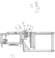
- the operation of the chip assembly tool 10 continues with the removal of the solder ball laden wafer "W" by the robotic arm 22 which is represented in figures 2 and 6 , and is roughly aligned in the pre-aligner in the load port 12. It is then transferred to the solder ball mount module 18 for optical alignment of the solder balls SB on the wafer W, as represented in figure 9 , figure 10 and figure 11.
- the wafer vacuum support chuck starts in the load position as it accepts the wafer from the robotic arm 22.
- the wafer plate has support pins with vacuum cups and several sets of independently controlled the vacuum channels or zones in the surface of the support plate.
- the wafer "W” is first loaded onto the support pins and secured with the vacuum cups. The pins recess into the vacuum support chuck.
- the stages actuated in the X, Y, and Z directions by linear actuators with push precision ball screws as represented in figure 6 .
- a high precision turntable also rotates the wafer "W” in the beta stage. All wafer support motions are computer-controlled through a proper circuit.
- the wafer stage then moves the wafer into the alignment window cutout 70 in the upper mounting plate 66, as shown in figure 6 .
- Two downward looking cameras 60 and 62, shown in figures 6 and 7 are stationed above the wafer "W” such that each camera is looking at a different predetermined location on the wafer.
- Each camera 60 and 62 is mounted to an independently operated linear drive 64, with a transverse orientation with respect to the mounting plate 66. Both actuators are, in turn, mounted on the gantry frame 74 shown in figure 6 and 7 , which gantry 74 can be actuated along the longitudinal axis of the mounting plate using one or two precision ballscrew actuators, wherein each camera 60 and 62 takes an image of a small portion of the wafer "W" and the proper computer, not shown, uses this information to determine the exact location of the wafer in the X, Y and theta configuration.
- the stage moves the wafer down, over and up through the second stencil window 78 in the mounting plate as shown in figure 6 .
- a rotary nomadic member 88 tilts the reservoir 102 and releases a predetermined volume of solder balls SB onto a primary distribution plate. The solder balls SB then move down through holes in several levels of secondary distribution plates and spread out further before finally being dispersed over the surface of the stencil 80.
- a brush head 96 represented in figure 8 is driven by an pneumatic actuator 98.
- the brush head 96 contains a series of sweeping members 100, such as wires, or pressurized perforated tubes with the perforations along its lower side, or the like, the sweeping members 100 being shown in figure 8 , which are amounted to the underside of the brush head 96 and such they protrude downwardly and make slight contact.
- the sweeping members 100 are wires, they are placed under slight tension so that a portion of each wire shown is drawn straight, parallel to the surface of the stencil 80. Straight portions of each sweeping member wire 100 span a distance greater than the diameter of the wafer "W" being processed. Keeping the wire 100 parallel with the stencil surface ensures uniform spacing between the wire 100 and the stencil 80.
- the brush head 96 While vibrating, the brush head 96 also translates back and forth parallel to the stencil 80 and perpendicularly to the wires or tubes 100 with a limited gross motion, to ensure at any point of the stencil 80 will be swept by a vibrating wire or pressurized tubes 100. Translating the sweeping member wires or pressurized tubes 100 also ensures no holes in the stencil 80 are covered the entire duration of the spreading operation which might prevent solder balls from filling those blocked holes. After spreading the solder balls SB, the holes in the stencil 80 should each contain one solder ball SB to be left upon a pad on the wafer once the wafer and the stencil are separated from one another.
- solder balls SB there may be extra solder balls SB on the stencil 80 which have not filled holes and these extra or excess solder balls need to be cleared before the wafer is lowered.
- the brush head 96 moves up and down out of the way and an air knife 50, shown in figure 4 , sweeps over the stencil 80 and pushes all extra solder balls SB to the backside of the stencil 80. Flow of air from the air knife 50 is strong enough to sweep away all solder balls not confined within a hole but not so strong as to dislodge the deposited solder balls.
- the air knife 50 pushes the balls under a flap, which flap acts as a one-way gate to prevent solder balls from rolling back onto the stencil 80.
- the solder balls collect on the back edge of the stencil 80 where they are sucked up by an overhead vacuum duct. From there the solder balls are conveyed to a collection vessel were all solder balls are separated from the airstream and stored for later reuse.
- a schematic representation of a brush head 21 and the solder ball mount module 18, is represented in figure 7A showing a funnel 23 which drops solder balls SB onto a perforated primary distribution plate 25 through which solder balls drop onto secondary distribution plates 27 and 29. Beneath the secondary distribution plates 27 and 29 there is shown the perforated stencil 31. Stencil 31 is shown above a wafer "W" arranged on the support chuck 33, the wafer W having arrangement of pads 35 thereon.
- a sweeper arrangement 37 is schematically represented attached to the brush shared 21.
- An inspection module 24, first shown in figure 2 is utilized to inspect the wafer "W” after ball placement thereon, to make sure that all solder balls are correctly positioned before being reflowed.
- the robot 22 loads a wafer "W”, as shown in figure 9A with mounted solder balls SB thereon onto a support pin arrangement 106, with vacuum cups thereon, as shown in figure 9 B .
- the pin arrangement 106 supports the wafer "W”
- they move down, driven by a pneumatic actuator and recess into the vacuum support plate 108 as shown in figure 9B .
- the support plate 108 contains several independently controlled sets of vacuum channels or zones, which grip the wafer once the support pins drop therefrom.
- Such repair station 198 is shown in figure 9D which comprises a base frame 210 supporting a control panel 212, a plurality of controls 214, a granite inspection slab 216 mounted on the base frame 210, a pick and place arm 220 mounted for movement in an X direction, a scanner drive assembly chuck 222 arranged for Y direction movement on the granite inspection slab 216, and an inspection camera assembly 200.
- An inspection light assembly 202 is shown in its up position, over the scanner drive assembly chuck 222.
- the inspection light assembly 202 when in the down position provides light for the inspection camera assembly 200 to view a wafer W on the scanner drive assembly chuck 222.
- the scanner drive assembly 222 moves the wafer under the camera assembly 200 allowing an image of the entire wafer to be generated.
- the inspection lights 202 may be moved into the up position allowing the pick and place arm 222 move over the wafer W on the scanner drive assembly chuck 222.
- the pick and place assembly as a needle hub arrangement 230 which includes a vacuum arrangement. As the pick and place assembly 220 hovers over the wafer it removes any misplaced solder balls and disposes of them.
- the pick and place assembly 220 When the wafer is repaired the pick and place assembly 220 will move out of the way, to the left as shown in figure 9D . Finally, the inspection light assembly 202 will move down allowing the inspection camera 200 and the scanner drive 222 to create a second image of the wafer. If no errors are found the wafer is removed from the inspection plus station transferred to the reflow module, and another wafer may be moved in for repair.
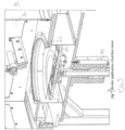
- the figures of figure 10 shows a reflow module open.
- the chamber is closed and sealed to the ambient environment. Wafers are moved from station to station within the chamber by a rotating carrier disc 128.
- the disc 128 has multiple slots for serial wafer processing. Each slot holds a carrier ring as shown in figure 5 and a support ring also shown in figure 5 wherein the wafer sits within the support ring.
- the reflow station or second station 124 of the reflow module 20 contains three computer-controlled heating elements: a bottom heater, a top heater and a ring heater are shown in figure 10 .
- the primary purpose of the bottom heaters to conductively heat a wafer "W" by making direct contact with the wafer assembly.
- the wafer assembly here consists of the wafer, the support ring and the clamp ring.
- the top heater is used for more gradual convective heating of the wafer within the tower - the tower being the portion of the reflow station above the desk.
- the ring heater is used to prevent thermal edge losses and improve the temperature uniformity of the wafer. A temperature gradient exists between the top and bottom heaters.
- the wafer may be positioned at different heights within the tower determines its rate of convective heating i.e. temperature, can be controlled.
- a hot wall conducts heat from the top heater in the ring heater and creates a more stable and gradual temperature gradient in the tower.
- the hot wall part may be the same piece which supports and transfers heat from the top heater.
- the wafer After the wafer is indexed from the load lock into the reflow station, it must be preheated. Preheating is most effectively accomplished by convectively heating the wafer in the tower, in proximity to the top heater. Though the top heater can be set to any temperature, it will normally be set significantly higher than the bottom heater. Therefore, the higher the wafers positioned in the reflow station, the hotter its surroundings become, and the faster it heats up. Elevator pins, driven by a servo motor, lift the wafer assembly and controls its height. The temperature sensors in the support ring contact the wafer and precisely monitor its temperature in real time. The combination of wafer temperature monitoring and wafer height control afford the user great control over the temperature profile of the wafer.
- a binder condenser system may be placed in line. This condensing system condenses the binder vapor removes it from the exhaust stream, preventing any binder vapor from reaching the facilities exhaust system.
Landscapes
- Engineering & Computer Science (AREA)
- Mechanical Engineering (AREA)
- Container, Conveyance, Adherence, Positioning, Of Wafer (AREA)
- Electric Connection Of Electric Components To Printed Circuits (AREA)
Claims (16)
- - Agencement unitaire d'assemblage de plaquettes (10) pour l'application de billes de soudure sur un substrat de plaquette (W) en vue d'une utilisation ultérieure dans l'industrie électronique, l'agencement d'assemblage de plaquettes (10) comprenant : un agencement de modules de traitement de plaquette, les modules de traitement de plaquette comprenant : un module de pré-alignement (14), pour la réception de plaquettes à traiter, un module de liant (16), un module de montage de billes de soudure (18) pour l'application d'une pluralité de billes de soudure (SB) sur la plaquette (W), un module d'inspection (24) comprenant un examen et une analyse, ainsi qu'un agencement d'insertion et d'extraction de billes de soudure (SB) mal appliquées déposées sur la plaquette (W), et un module de refusion (20) pour chauffer et fixer les billes de soudure (SB) sur un agencement de plots sur la plaquette (W), caractérisé par le fait que :un robot central de manipulation de plaquette (22) relie et entretient lesdits modules de traitement de plaquette (14, 16, 18, 20) pour constituer un système unitaire ;ledit module de liant (16) est configuré pour appliquer un liant fluide sans flux (B) sur une surface supérieure de la plaquette (W), ledit liant fluide sans flux (B) étant configuré pour s'évaporer complètement de ladite surface supérieure de ladite plaquette (W) à une température élevée, ledit module de liant (16) comprend en outre une ou plusieurs buses (44) configurées pour être balayées sur la plaquette (W) une ou plusieurs fois, et pour distribuer de manière uniforme le liant fluide (B) par pulvérisation de celui-ci suivant un motif en éventail approximativement normal à la direction de balayage, et ledit module de liant (16) comprend en outre une lame d'air (50), configurée pour balayer puis projeter un rideau d'air comprimé sur ladite surface supérieure de ladite plaquette (W) une fois que ledit liant fluide sans flux (B) a été pulvérisé, ledit rideau d'air comprimé provenant de ladite lame d'air (50) pour étaler et amincir ledit liant sans flux (B) appliqué sur la surface supérieure de ladite plaquette (W) laissant derrière lui un film uniforme de liant fluide sans flux (B) sur ladite surface supérieure de ladite plaquette (W).
- - Agencement d'assemblage de plaquettes (10) selon la revendication 1, dans lequel, en utilisation, le liant fluide sans flux (B) est appliqué à la plaquette (W) à température ambiante ou à une température élevée, l'agencement comprenant en outre un portique commandé par ordinateur (46) disposé de manière mobile au-dessus d'une plaquette supportée par celui-ci, et le portique (46) supportant un agencement de buses comprenant la ou les buses, et l'agencement comprenant en outre un collecteur et un port de drainage, de telle sorte qu'en utilisation un excès de liant fluide sans flux (B) est collecté et utilisé pour une autre plaquette.
- - Agencement d'assemblage de plaquettes (10) selon la revendication 2, dans lequel le module de montage de billes de soudure (18) comprend des plaques d'alignement de billes de soudure foraminées, de telle sorte qu'une pluralité de billes de soudure (SB) sont disposées suivant un réseau, sur un motif espacé d'emplacements d'engagement de billes de soudure sur la plaquette (W) une fois que les billes de soudure (SB) ont été filtrées à travers un réseau vertical des plaques d'alignement de billes de soudure foraminées disposées de manière mobile au-dessus de la plaquette (W).
- - Agencement d'assemblage de plaquettes (10) selon la revendication 3, dans lequel une lame d'air supplémentaire (50) est configurée pour être entraînée transversalement en travers du réseau de billes de soudure (SB) sur la surface supérieure de la plaquette (W) de façon à déplacer toute bille de soudure (SB) superflue à partir de la surface de la plaquette (W).
- - Agencement d'assemblage de plaquettes (10) selon la revendication 4, dans lequel un canal unidirectionnel est prévu de telle sorte qu'en utilisation toute bille de soudure (SB) superflue est acheminée jusqu'au canal unidirectionnel en vue d'une collecte et d'une réutilisation ultérieure sur une autre plaquette.
- - Agencement d'assemblage de plaquettes (10) selon la revendication 1, l'agencement comprenant en outre : un module de port de chargement (2) pour la réception des plaquettes à traiter, un moyen d'aspiration à tiges de support (30) pour maintenir la plaquette (W), le module de liant (16) pour maintenir, en utilisation, chaque plaquette (W) par le moyen d'aspiration à tiges de support pendant l'opération de dépôt de liant par pulvérisation et de nettoyage de liant ; un module de pré-alignement (14) ; un module de montage de billes de soudure (18) avec un moyen de support de tiges à ventouse (30), un pochoir de distribution de billes de soudure (80) et un réservoir de distribution de billes de soudure (102) au-dessus du pochoir (80) pour la libération contrôlée de billes de soudure (SB) sur la plaquette (W) située en dessous ; un moyen de récupération de billes de soudure inappropriées et d'excès de liant ; une pluralité de caméras pour un examen d'alignement optique ; et un module de refusion à trois postes (20) pour le traitement thermique d'une plaquette chargée (W).
- - Agencement d'assemblage de plaquettes (10) selon la revendication 6, dans lequel un portique commandé par ordinateur (46) est disposé de manière mobile au-dessus d'une plaquette supportée par celui-ci et supporte un agencement de buses comprenant la ou les buses de telle sorte qu'en utilisation le liant fluide sans flux (B) est appliqué sur la plaquette (W) par l'agencement de buses.
- - Agencement d'assemblage de plaquettes (10) selon la revendication 7, dans lequel, en utilisation, une pluralité de billes de soudure (SB) sont disposées en un réseau, sur un motif espacé d'emplacements d'engagement de billes de soudure sur la plaquette (W) une fois que les billes de soudure (SB) sont tombées à travers un réseau vertical de plaques d'alignement de billes de soudure foraminées disposées vibratoirement au-dessus de la plaquette (W).
- - Agencement d'assemblage de plaquettes (10) selon la revendication 8, dans lequel une autre lame d'air (50) est prévue sur le portique (46) et est configurée pour être entraînée transversalement en travers du réseau de billes de soudure (SB) sur la surface supérieure de la plaquette (W) de façon à déplacer toute bille de soudure (SB) superflue à partir de la surface de la plaquette (W).
- - Agencement d'assemblage de plaquettes (10) selon la revendication 9, dans lequel un canal unidirectionnel est prévu de telle sorte qu'en utilisation toute bille de soudure (SB) superflue est acheminée sous une vanne unidirectionnelle jusqu'au canal unidirectionnel en vue d'une collecte et d'une réutilisation ultérieure sur une autre plaquette.
- - Procédé d'utilisation d'une pluralité de billes de soudure (SB) dans un agencement d'assemblage de plaquettes (10) pour l'application de la pluralité de billes de soudure (SB) sur une plaquette (W) en vue d'une utilisation ultérieure dans l'industrie électronique, caractérisé par le fait que le procédé comprend :appliquer un liant fluide sans flux (B) sur une surface supérieure de la plaquette (W), ledit liant fluide sans flux (B) étant configuré pour s'évaporer complètement de ladite surface supérieure de ladite plaquette (W) à une température élevée, ledit liant fluide sans flux (B) étant appliqué par une ou plusieurs buses (44) balayant la plaquette (W) une ou plusieurs fois, pour distribuer de manière uniforme le liant fluide (B) par pulvérisation de celui-ci suivant un motif en éventail approximativement normal à la direction de balayage, et utiliser une lame d'air (50) par balayage puis projection d'un rideau d'air comprimé en travers de ladite surface supérieure de ladite plaquette (W) une fois que ledit liant fluide sans flux (B) a été pulvérisé et réparti de manière uniforme sur la surface supérieure de ladite plaquette (W), ledit rideau d'air comprimé provenant de ladite lame d'air (50) pour étaler et amincir le liant fluide sans flux (B) appliqué sur la surface supérieure de ladite plaquette (W) laissant derrière lui un film uniforme de liant fluide sans flux (B) sur ladite surface supérieure de ladite plaquette (W) ;placer une cartouche de billes de soudure préchargées (SB) dans une unité de réception sur l'agencement d'assemblage de plaquettes (10) ; libérer un nombre limité de billes de soudure (10) dans une voie de distribution dans l'agencement d'assemblage de plaquettes (10) ; faire tomber les billes de soudure (SB) à travers un entonnoir (23) et dans une coupelle de distribution ; distribuer les billes de soudure (SB) à partir de la coupelle de distribution sur une plaque de distribution primaire (25) ; faire passer les billes de soudure (SB) à travers la plaque de distribution primaire (25) et sur une pluralité de plaques de distribution secondaires (27,29) ; faire tomber les billes de soudure (SB) à partir des plaques de distribution secondaires (27, 29) sur un pochoir (80), une plaquette (W) étant disposée immédiatement sous le pochoir (80) ; balayer les billes de soudure (SB) dans un réseau de trous de réception de billes de soudure dans le pochoir (80) ; abaisser une plaquette chargée de billes de soudure (W) sur un bras robotique ; et transférer la plaquette chargée de billes de soudure (W) sur le bras robotique (22) dans un module d'inspection (24).
- - Procédé d'utilisation d'une pluralité de billes de soudure (SB) dans un agencement d'assemblage de plaquettes (10) selon la revendication 11, dans lequel les billes de soudure (SB) sont balayées en travers du pochoir (80) par un agencement de balayage (37) pour permettre aux billes de soudure (SB) de remplir le réseau de trous de réception de billes de soudure dans le pochoir (80).
- - Procédé d'utilisation d'une pluralité de billes de soudure (SB) dans un agencement d'assemblage de plaquettes (10) selon la revendication 12, dans lequel l'agencement de balayage (37) déplaçant les billes de soudure (SB) est un aérographe.
- - Procédé d'utilisation d'une pluralité de billes de soudure (SB) dans un agencement d'assemblage de plaquettes (10) selon la revendication 12, dans lequel l'agencement de balayage (37) déplaçant les billes de soudure (SB) est une brosse métallique.
- - Procédé d'utilisation d'une pluralité de billes de soudure (SB) dans un agencement d'assemblage de plaquettes (10) selon la revendication 11, dans lequel les plaques de distribution primaire et secondaires (25, 27, 29) vibrent lors du passage des billes de soudure (SB) à travers celles-ci.
- - Procédé de fabrication d'un assemblage de puces dans un système unitaire d'assemblage de plaquettes, destiné à être utilisé dans l'industrie électronique, comprenant les étapes :traiter en utilisant toutes les étapes du procédé tel que défini dans la revendication 11 ;retirer la plaquette (W) d'un boîtier universel à ouverture frontale par un robot (22), la plaquette (W) étant délivrée à un pré-aligneur en vue d'un centrage ;transférer la plaquette (W) à un poste de liant (16) par le robot (22), le fluide de liant (B) étant appliqué sur la plaquette (W) ;amener la plaquette (W) par le robot (22) jusqu'à un poste de montage de billes de soudure (18) sur un mandrin à une première ouverture de position d'entretien de plaquette ;aligner la plaquette (W) par un agencement de caméras pour une orientation ultérieure de la plaquette (W) avec un motif de trous de pochoir ;transférer la plaquette (W) à une seconde ouverture de position d'entretien de plaquette où se trouve le pochoir (80) ;déplacer un mandrin de support de plaquette vers le haut pour lever la plaquette très près du pochoir (80), à une distance inférieure à un diamètre de bille de soudure ;vérifier un alignement de plaquette par un agencement de vérification par caméra sur une tête de bille de soudure suspendue faisant partie d'un portique mobile (46), en visualisant la plaquette (W) à travers le pochoir (80) pour identifier des repères sur la plaquette (W) ;déplacer une tête de bille de soudure, une fois l'alignement de plaquette vérifié, dans une position appropriée sur la plaquette (W) ;distribuer des billes de soudure (SB) à partir d'un réservoir de billes de soudure sur la tête de bille de soudure ;approcher la tête de bille de soudure du pochoir (80) ;activer la tête de bille de soudure pour placer une brosse (96) sur le pochoir (80) ;déplacer la brosse (96) sur la plaquette (W) d'avant en arrière, sans toucher la plaquette (W), pour pousser des billes de soudure (SB) dans des trous de la plaquette (W) ;souffler de l'air sec comprimé à l'aide d'une lame d'air (50) sur le portique (46) à travers le pochoir (80) de façon à récupérer toute bille de soudure (SB) non chargée, dans une chambre de collecte sous vide en vue d'une réutilisation ultérieure ;délivrée de manière robotisée la plaquette chargée de billes de soudure (W) à un mandrin dans un premier poste/poste de verrouillage de charge (122) dans un module de refusion (20), et purger l'oxygène du premier poste ;maintenir la plaquette (W) sur le mandrin par un vide, et faire avancer le mandrin de manière rotative jusqu'à un deuxième poste (124) en vue d'un préchauffage ;surélever la plaquette (W) à travers le mandrin sur des élévateurs jusqu'à un anneau, au sommet d'une chambre du deuxième poste (124), pour atteindre la température de refusion pré-fondue la plus élevée ;abaisser la plaquette (W) par l'élévateur à travers le mandrin, pour ramener la plaquette en repos sur le mandrin de façon à permettre à la plaquette (W) d'atteindre une température de refusion contrôlée, la plaquette (W) étant ensuite tournée jusqu'à un troisième poste (126) dans le module de refusion (20) ;séparer la plaquette (W) du mandrin par une plaque à vide, la plaquette (W) étant refroidie par de l'azote sous la plaque et au-dessus de la plaquette, un vide transmis à travers le mandrin maintenant la plaquette (W) à plat sur celui-ci ;faire tourner le mandrin jusqu' au premier poste (122) pour le déchargement d'une plaquette finie (W).
Applications Claiming Priority (2)
| Application Number | Priority Date | Filing Date | Title |
|---|---|---|---|
| US201862766076P | 2018-09-28 | 2018-09-28 | |
| PCT/US2019/053421 WO2020069294A1 (fr) | 2018-09-28 | 2019-09-27 | Agencement de fabrication de puces à modules multiples |
Publications (5)
| Publication Number | Publication Date |
|---|---|
| EP3857592A1 EP3857592A1 (fr) | 2021-08-04 |
| EP3857592A4 EP3857592A4 (fr) | 2022-07-13 |
| EP3857592B1 true EP3857592B1 (fr) | 2023-12-13 |
| EP3857592C0 EP3857592C0 (fr) | 2023-12-13 |
| EP3857592B8 EP3857592B8 (fr) | 2024-01-24 |
Family
ID=69953370
Family Applications (1)
| Application Number | Title | Priority Date | Filing Date |
|---|---|---|---|
| EP19865166.3A Active EP3857592B8 (fr) | 2018-09-28 | 2019-09-27 | Agencement de fabrication de puces à modules multiples |
Country Status (5)
| Country | Link |
|---|---|
| EP (1) | EP3857592B8 (fr) |
| JP (2) | JP2022514137A (fr) |
| KR (1) | KR102752911B1 (fr) |
| CN (1) | CN112789705B (fr) |
| WO (1) | WO2020069294A1 (fr) |
Families Citing this family (5)
| Publication number | Priority date | Publication date | Assignee | Title |
|---|---|---|---|---|
| US11440117B2 (en) * | 2019-09-27 | 2022-09-13 | Jian Zhang | Multiple module chip manufacturing arrangement |
| CN114378388B (zh) * | 2022-02-11 | 2023-06-16 | 张云柱 | 一种在背光源中全自动装配支撑件的方法 |
| CN114566452B (zh) * | 2022-04-29 | 2022-07-15 | 武汉飞恩微电子有限公司 | 基座与芯片黏合装置及含其的压力传感器自动封装生产线 |
| CN115274513B (zh) * | 2022-09-05 | 2025-09-09 | 万昇半导体科技(深圳)有限公司 | 一种自动植球设备及自动植球方法 |
| CN120784190A (zh) * | 2025-08-22 | 2025-10-14 | 盛红晔半导体科技(上海)有限公司 | 一种基于堆叠式负载锁的晶圆处理系统及方法 |
Citations (1)
| Publication number | Priority date | Publication date | Assignee | Title |
|---|---|---|---|---|
| US6413850B1 (en) * | 1999-11-18 | 2002-07-02 | Hitachi, Ltd. | Method of forming bumps |
Family Cites Families (37)
| Publication number | Priority date | Publication date | Assignee | Title |
|---|---|---|---|---|
| JPS61172669A (ja) * | 1985-01-25 | 1986-08-04 | Tamura Seisakusho Co Ltd | 自動はんだ付けシステムの制御方法 |
| US4848641A (en) * | 1988-07-05 | 1989-07-18 | Hughes Aircraft Company | Flux dispenser |
| JP3430864B2 (ja) * | 1997-06-30 | 2003-07-28 | 松下電器産業株式会社 | 導電性ボールの移載方法 |
| US6182356B1 (en) * | 1997-11-24 | 2001-02-06 | International Business Machines Corporation | Apparatus for solder ball mold loading |
| US6268275B1 (en) * | 1998-10-08 | 2001-07-31 | Micron Technology, Inc. | Method of locating conductive spheres utilizing screen and hopper of solder balls |
| JP4959056B2 (ja) * | 1999-03-17 | 2012-06-20 | ノバテック エスア | ボールをボール受容要素中のアパーチャに充填するための充填デバイスおよび方法 |
| US6412680B1 (en) * | 2000-09-26 | 2002-07-02 | Agere Systems Guardian Corp. | Dual-in-line BGA ball mounter |
| JP2003303926A (ja) * | 2002-04-09 | 2003-10-24 | Misuzu Kogyo:Kk | Bga製品基板の製造装置、及びその製造方法 |
| US9226407B2 (en) * | 2002-07-01 | 2015-12-29 | Semigear Inc | Reflow treating unit and substrate treating apparatus |
| JP4505783B2 (ja) * | 2003-01-31 | 2010-07-21 | 日立金属株式会社 | 半田バンプの製造方法及び製造装置 |
| JP4412915B2 (ja) * | 2003-05-09 | 2010-02-10 | 富士機械製造株式会社 | フラックス転写装置及びフラックス転写方法 |
| JP2006135014A (ja) * | 2004-11-04 | 2006-05-25 | Waida Seisakusho:Kk | 半田ボール発射装置及び半田ボール搭載システム |
| JP4560682B2 (ja) * | 2005-04-28 | 2010-10-13 | 澁谷工業株式会社 | 導電性ボール搭載装置 |
| CN101123172A (zh) * | 2006-08-11 | 2008-02-13 | 日月光半导体制造股份有限公司 | 助焊剂残留的去除方法 |
| WO2008063138A2 (fr) * | 2006-11-22 | 2008-05-29 | Rokko Ventures Pte Ltd | Appareil et procédé améliorés de montage de billes |
| JP5008452B2 (ja) * | 2007-05-08 | 2012-08-22 | 新日鉄マテリアルズ株式会社 | はんだボールの搭載方法及び搭載装置 |
| US20080296355A1 (en) * | 2007-05-31 | 2008-12-04 | Texas Instruments Incorporated | Direct ball dispenser |
| JP4503053B2 (ja) * | 2007-07-24 | 2010-07-14 | 新光電気工業株式会社 | 導電性ボールの搭載装置および搭載方法 |
| JP5273428B2 (ja) * | 2007-08-29 | 2013-08-28 | 澁谷工業株式会社 | 導電性ボール搭載装置 |
| JP5076922B2 (ja) * | 2008-01-25 | 2012-11-21 | 株式会社日立プラントテクノロジー | ハンダボール印刷装置 |
| JP2009071332A (ja) * | 2008-12-15 | 2009-04-02 | Athlete Fa Kk | 導電性ボールを搭載するための装置 |
| KR100977163B1 (ko) * | 2009-03-23 | 2010-08-20 | 덕산하이메탈(주) | 솔더 접착제와 그 제조 방법 및 이를 포함하는 전자 장치 |
| KR101141921B1 (ko) * | 2011-09-09 | 2012-05-07 | 주식회사 고려반도체시스템 | 미리 정해진 패턴으로 분포된 다수의 수용부에 솔더볼을 안착시키는 방법 및 이에 사용되는 장치 |
| KR101508039B1 (ko) * | 2012-05-17 | 2015-04-06 | 삼성전기주식회사 | 솔더볼 공급장치 |
| KR101410171B1 (ko) * | 2013-01-16 | 2014-06-30 | (주) 에스에스피 | 웨이퍼 범핑 장비 및 이를 이용한 범핑 방법 |
| US20150034702A1 (en) * | 2013-08-01 | 2015-02-05 | Semigear Inc | Apparatus & method for treating substrate |
| JP2015073032A (ja) * | 2013-10-03 | 2015-04-16 | 株式会社日立製作所 | 電極形成装置及び電極形成方法 |
| JP2015082630A (ja) * | 2013-10-24 | 2015-04-27 | 有限会社ヨコタテクニカ | 粉末半田を使った半田付け方法及びフラックスレス連続リフロー炉 |
| US9694436B2 (en) * | 2013-11-04 | 2017-07-04 | Veeco Precision Surface Processing Llc | System and method for flux coat, reflow and clean |
| CN103606527B (zh) * | 2013-12-09 | 2016-01-13 | 上海微松工业自动化有限公司 | 半自动晶圆植球设备 |
| JP6320066B2 (ja) * | 2014-02-13 | 2018-05-09 | イビデン株式会社 | ボール搭載用マスクおよびボール搭載装置 |
| CN203786831U (zh) * | 2014-02-14 | 2014-08-20 | 北京莱柏锐科技有限公司 | 一种图书馆借还机 |
| US10242968B2 (en) * | 2015-11-05 | 2019-03-26 | Massachusetts Institute Of Technology | Interconnect structure and semiconductor structures for assembly of cryogenic electronic packages |
| US10894935B2 (en) * | 2015-12-04 | 2021-01-19 | Samsung Electronics Co., Ltd. | Composition for removing silicone resins and method of thinning substrate by using the same |
| US10879102B2 (en) * | 2017-08-07 | 2020-12-29 | Boston Process Technologies, Inc | Flux-free solder ball mount arrangement |
| CN110998813B (zh) * | 2017-08-07 | 2023-12-01 | 柏锐科技有限公司 | 热壁无助焊剂焊球处理装置 |
| CN108321093B (zh) * | 2018-02-02 | 2019-03-29 | 英特尔产品(成都)有限公司 | 用于清理焊球模板的方法 |
-
2019
- 2019-09-27 JP JP2021515489A patent/JP2022514137A/ja active Pending
- 2019-09-27 WO PCT/US2019/053421 patent/WO2020069294A1/fr not_active Ceased
- 2019-09-27 CN CN201980062731.XA patent/CN112789705B/zh active Active
- 2019-09-27 EP EP19865166.3A patent/EP3857592B8/fr active Active
- 2019-09-27 KR KR1020217011998A patent/KR102752911B1/ko active Active
-
2024
- 2024-06-28 JP JP2024105081A patent/JP7839225B2/ja active Active
Patent Citations (1)
| Publication number | Priority date | Publication date | Assignee | Title |
|---|---|---|---|---|
| US6413850B1 (en) * | 1999-11-18 | 2002-07-02 | Hitachi, Ltd. | Method of forming bumps |
Also Published As
| Publication number | Publication date |
|---|---|
| KR20210058962A (ko) | 2021-05-24 |
| CN112789705B (zh) | 2024-07-26 |
| JP7839225B2 (ja) | 2026-04-01 |
| JP2024150475A (ja) | 2024-10-23 |
| WO2020069294A1 (fr) | 2020-04-02 |
| EP3857592A1 (fr) | 2021-08-04 |
| CN112789705A (zh) | 2021-05-11 |
| WO2020069294A4 (fr) | 2020-06-18 |
| JP2022514137A (ja) | 2022-02-10 |
| EP3857592B8 (fr) | 2024-01-24 |
| KR102752911B1 (ko) | 2025-01-10 |
| EP3857592A4 (fr) | 2022-07-13 |
| EP3857592C0 (fr) | 2023-12-13 |
Similar Documents
| Publication | Publication Date | Title |
|---|---|---|
| EP3857592B1 (fr) | Agencement de fabrication de puces à modules multiples | |
| US11440117B2 (en) | Multiple module chip manufacturing arrangement | |
| CN111095504B (zh) | 无助焊剂焊球安装装置 | |
| US11972968B2 (en) | Fluxless gang die bonding arrangement | |
| KR102501497B1 (ko) | 턴테이블 방식의 프로브핀 레이저 본딩장치 | |
| JPH0964104A (ja) | チップの搭載装置および搭載方法 | |
| WO2012026152A1 (fr) | Système de collage, système de traitement de substrat, procédé de collage, programme, et support de stockage informatique | |
| CN104701222B (zh) | 一种面阵凸点植球工艺的补球装置及方法 | |
| JP5606780B2 (ja) | 半導体装置の製造装置 | |
| JP4064795B2 (ja) | 電子部品実装装置 | |
| KR20250056779A (ko) | 전자부품 테스트용 핸들러 | |
| KR20250056767A (ko) | 전자부품 테스트용 핸들러 | |
| KR102819271B1 (ko) | 본딩장치 및 본딩방법 | |
| JPH06267916A (ja) | 半導体ウェーハの接着装置 | |
| JP7579295B2 (ja) | 実装システム | |
| JP4105022B2 (ja) | 導電性ボールの配列搭載方法および装置ならびにバンプ形成方法および装置 | |
| JP2026061481A (ja) | 実装装置および実装方法 |
Legal Events
| Date | Code | Title | Description |
|---|---|---|---|
| STAA | Information on the status of an ep patent application or granted ep patent |
Free format text: STATUS: THE INTERNATIONAL PUBLICATION HAS BEEN MADE |
|
| PUAI | Public reference made under article 153(3) epc to a published international application that has entered the european phase |
Free format text: ORIGINAL CODE: 0009012 |
|
| STAA | Information on the status of an ep patent application or granted ep patent |
Free format text: STATUS: REQUEST FOR EXAMINATION WAS MADE |
|
| 17P | Request for examination filed |
Effective date: 20210322 |
|
| AK | Designated contracting states |
Kind code of ref document: A1 Designated state(s): AL AT BE BG CH CY CZ DE DK EE ES FI FR GB GR HR HU IE IS IT LI LT LU LV MC MK MT NL NO PL PT RO RS SE SI SK SM TR |
|
| DAV | Request for validation of the european patent (deleted) | ||
| DAX | Request for extension of the european patent (deleted) | ||
| A4 | Supplementary search report drawn up and despatched |
Effective date: 20220610 |
|
| RIC1 | Information provided on ipc code assigned before grant |
Ipc: H01L 21/683 20060101ALI20220603BHEP Ipc: B23K 3/08 20060101ALI20220603BHEP Ipc: B23K 3/06 20060101ALI20220603BHEP Ipc: B23K 1/20 20060101ALI20220603BHEP Ipc: B23K 1/008 20060101ALI20220603BHEP Ipc: B23K 1/00 20060101ALI20220603BHEP Ipc: B25J 15/06 20060101ALI20220603BHEP Ipc: B25J 11/00 20060101ALI20220603BHEP Ipc: H01L 21/67 20060101ALI20220603BHEP Ipc: H01L 21/68 20060101AFI20220603BHEP |
|
| REG | Reference to a national code |
Ipc: H01L0021680000 Ref country code: DE Ref legal event code: R079 Ref document number: 602019043383 Country of ref document: DE Free format text: PREVIOUS MAIN CLASS: H01L0021020000 Ipc: H01L0021680000 |
|
| GRAP | Despatch of communication of intention to grant a patent |
Free format text: ORIGINAL CODE: EPIDOSNIGR1 |
|
| STAA | Information on the status of an ep patent application or granted ep patent |
Free format text: STATUS: GRANT OF PATENT IS INTENDED |
|
| RIC1 | Information provided on ipc code assigned before grant |
Ipc: H01L 21/683 20060101ALI20230525BHEP Ipc: B23K 3/08 20060101ALI20230525BHEP Ipc: B23K 3/06 20060101ALI20230525BHEP Ipc: B23K 1/20 20060101ALI20230525BHEP Ipc: B23K 1/008 20060101ALI20230525BHEP Ipc: B23K 1/00 20060101ALI20230525BHEP Ipc: B25J 15/06 20060101ALI20230525BHEP Ipc: B25J 11/00 20060101ALI20230525BHEP Ipc: H01L 21/67 20060101ALI20230525BHEP Ipc: H01L 21/68 20060101AFI20230525BHEP |
|
| INTG | Intention to grant announced |
Effective date: 20230626 |
|
| GRAS | Grant fee paid |
Free format text: ORIGINAL CODE: EPIDOSNIGR3 |
|
| GRAA | (expected) grant |
Free format text: ORIGINAL CODE: 0009210 |
|
| STAA | Information on the status of an ep patent application or granted ep patent |
Free format text: STATUS: THE PATENT HAS BEEN GRANTED |
|
| REG | Reference to a national code |
Ref country code: DE Ref legal event code: R081 Ref document number: 602019043383 Country of ref document: DE Owner name: SHARPACK TECHNOLOGY PTE. LTD., SG Free format text: FORMER OWNER: BOSTON PROCESS TECHNOLOGIES, INC., PEABODY, MA, US |
|
| AK | Designated contracting states |
Kind code of ref document: B1 Designated state(s): AL AT BE BG CH CY CZ DE DK EE ES FI FR GB GR HR HU IE IS IT LI LT LU LV MC MK MT NL NO PL PT RO RS SE SI SK SM TR |
|
| REG | Reference to a national code |
Ref country code: GB Ref legal event code: FG4D |
|
| REG | Reference to a national code |
Ref country code: CH Ref legal event code: EP |
|
| REG | Reference to a national code |
Ref country code: DE Ref legal event code: R096 Ref document number: 602019043383 Country of ref document: DE |
|
| RAP2 | Party data changed (patent owner data changed or rights of a patent transferred) |
Owner name: SHARPACK TECHNOLOGY PTE. LTD. |
|
| REG | Reference to a national code |
Ref country code: CH Ref legal event code: PK Free format text: BERICHTIGUNG B8 |
|
| REG | Reference to a national code |
Ref country code: IE Ref legal event code: FG4D |
|
| U01 | Request for unitary effect filed |
Effective date: 20231213 |
|
| U07 | Unitary effect registered |
Designated state(s): AT BE BG DE DK EE FI FR IT LT LU LV MT NL PT SE SI Effective date: 20231219 |
|
| PG25 | Lapsed in a contracting state [announced via postgrant information from national office to epo] |
Ref country code: GR Free format text: LAPSE BECAUSE OF FAILURE TO SUBMIT A TRANSLATION OF THE DESCRIPTION OR TO PAY THE FEE WITHIN THE PRESCRIBED TIME-LIMIT Effective date: 20240314 |
|
| PG25 | Lapsed in a contracting state [announced via postgrant information from national office to epo] |
Ref country code: ES Free format text: LAPSE BECAUSE OF FAILURE TO SUBMIT A TRANSLATION OF THE DESCRIPTION OR TO PAY THE FEE WITHIN THE PRESCRIBED TIME-LIMIT Effective date: 20231213 |
|
| PG25 | Lapsed in a contracting state [announced via postgrant information from national office to epo] |
Ref country code: GR Free format text: LAPSE BECAUSE OF FAILURE TO SUBMIT A TRANSLATION OF THE DESCRIPTION OR TO PAY THE FEE WITHIN THE PRESCRIBED TIME-LIMIT Effective date: 20240314 Ref country code: ES Free format text: LAPSE BECAUSE OF FAILURE TO SUBMIT A TRANSLATION OF THE DESCRIPTION OR TO PAY THE FEE WITHIN THE PRESCRIBED TIME-LIMIT Effective date: 20231213 |
|
| PG25 | Lapsed in a contracting state [announced via postgrant information from national office to epo] |
Ref country code: RS Free format text: LAPSE BECAUSE OF FAILURE TO SUBMIT A TRANSLATION OF THE DESCRIPTION OR TO PAY THE FEE WITHIN THE PRESCRIBED TIME-LIMIT Effective date: 20231213 Ref country code: NO Free format text: LAPSE BECAUSE OF FAILURE TO SUBMIT A TRANSLATION OF THE DESCRIPTION OR TO PAY THE FEE WITHIN THE PRESCRIBED TIME-LIMIT Effective date: 20240313 Ref country code: HR Free format text: LAPSE BECAUSE OF FAILURE TO SUBMIT A TRANSLATION OF THE DESCRIPTION OR TO PAY THE FEE WITHIN THE PRESCRIBED TIME-LIMIT Effective date: 20231213 |
|
| PG25 | Lapsed in a contracting state [announced via postgrant information from national office to epo] |
Ref country code: IS Free format text: LAPSE BECAUSE OF FAILURE TO SUBMIT A TRANSLATION OF THE DESCRIPTION OR TO PAY THE FEE WITHIN THE PRESCRIBED TIME-LIMIT Effective date: 20240413 |
|
| PG25 | Lapsed in a contracting state [announced via postgrant information from national office to epo] |
Ref country code: CZ Free format text: LAPSE BECAUSE OF FAILURE TO SUBMIT A TRANSLATION OF THE DESCRIPTION OR TO PAY THE FEE WITHIN THE PRESCRIBED TIME-LIMIT Effective date: 20231213 |
|
| PG25 | Lapsed in a contracting state [announced via postgrant information from national office to epo] |
Ref country code: SK Free format text: LAPSE BECAUSE OF FAILURE TO SUBMIT A TRANSLATION OF THE DESCRIPTION OR TO PAY THE FEE WITHIN THE PRESCRIBED TIME-LIMIT Effective date: 20231213 |
|
| PG25 | Lapsed in a contracting state [announced via postgrant information from national office to epo] |
Ref country code: SM Free format text: LAPSE BECAUSE OF FAILURE TO SUBMIT A TRANSLATION OF THE DESCRIPTION OR TO PAY THE FEE WITHIN THE PRESCRIBED TIME-LIMIT Effective date: 20231213 Ref country code: SK Free format text: LAPSE BECAUSE OF FAILURE TO SUBMIT A TRANSLATION OF THE DESCRIPTION OR TO PAY THE FEE WITHIN THE PRESCRIBED TIME-LIMIT Effective date: 20231213 Ref country code: RO Free format text: LAPSE BECAUSE OF FAILURE TO SUBMIT A TRANSLATION OF THE DESCRIPTION OR TO PAY THE FEE WITHIN THE PRESCRIBED TIME-LIMIT Effective date: 20231213 Ref country code: IS Free format text: LAPSE BECAUSE OF FAILURE TO SUBMIT A TRANSLATION OF THE DESCRIPTION OR TO PAY THE FEE WITHIN THE PRESCRIBED TIME-LIMIT Effective date: 20240413 Ref country code: CZ Free format text: LAPSE BECAUSE OF FAILURE TO SUBMIT A TRANSLATION OF THE DESCRIPTION OR TO PAY THE FEE WITHIN THE PRESCRIBED TIME-LIMIT Effective date: 20231213 |
|
| PG25 | Lapsed in a contracting state [announced via postgrant information from national office to epo] |
Ref country code: PL Free format text: LAPSE BECAUSE OF FAILURE TO SUBMIT A TRANSLATION OF THE DESCRIPTION OR TO PAY THE FEE WITHIN THE PRESCRIBED TIME-LIMIT Effective date: 20231213 |
|
| PG25 | Lapsed in a contracting state [announced via postgrant information from national office to epo] |
Ref country code: PL Free format text: LAPSE BECAUSE OF FAILURE TO SUBMIT A TRANSLATION OF THE DESCRIPTION OR TO PAY THE FEE WITHIN THE PRESCRIBED TIME-LIMIT Effective date: 20231213 |
|
| REG | Reference to a national code |
Ref country code: DE Ref legal event code: R097 Ref document number: 602019043383 Country of ref document: DE |
|
| PLBE | No opposition filed within time limit |
Free format text: ORIGINAL CODE: 0009261 |
|
| STAA | Information on the status of an ep patent application or granted ep patent |
Free format text: STATUS: NO OPPOSITION FILED WITHIN TIME LIMIT |
|
| U20 | Renewal fee for the european patent with unitary effect paid |
Year of fee payment: 6 Effective date: 20240930 |
|
| 26N | No opposition filed |
Effective date: 20240916 |
|
| PG25 | Lapsed in a contracting state [announced via postgrant information from national office to epo] |
Ref country code: MC Free format text: LAPSE BECAUSE OF FAILURE TO SUBMIT A TRANSLATION OF THE DESCRIPTION OR TO PAY THE FEE WITHIN THE PRESCRIBED TIME-LIMIT Effective date: 20231213 |
|
| REG | Reference to a national code |
Ref country code: CH Ref legal event code: PL |
|
| GBPC | Gb: european patent ceased through non-payment of renewal fee |
Effective date: 20240927 |
|
| PG25 | Lapsed in a contracting state [announced via postgrant information from national office to epo] |
Ref country code: GB Free format text: LAPSE BECAUSE OF NON-PAYMENT OF DUE FEES Effective date: 20240927 |
|
| PG25 | Lapsed in a contracting state [announced via postgrant information from national office to epo] |
Ref country code: CH Free format text: LAPSE BECAUSE OF NON-PAYMENT OF DUE FEES Effective date: 20240930 |
|
| PG25 | Lapsed in a contracting state [announced via postgrant information from national office to epo] |
Ref country code: IE Free format text: LAPSE BECAUSE OF NON-PAYMENT OF DUE FEES Effective date: 20240927 |
|
| U20 | Renewal fee for the european patent with unitary effect paid |
Year of fee payment: 7 Effective date: 20250929 |
|
| PG25 | Lapsed in a contracting state [announced via postgrant information from national office to epo] |
Ref country code: CY Free format text: LAPSE BECAUSE OF FAILURE TO SUBMIT A TRANSLATION OF THE DESCRIPTION OR TO PAY THE FEE WITHIN THE PRESCRIBED TIME-LIMIT; INVALID AB INITIO Effective date: 20190927 |
|
| PG25 | Lapsed in a contracting state [announced via postgrant information from national office to epo] |
Ref country code: HU Free format text: LAPSE BECAUSE OF FAILURE TO SUBMIT A TRANSLATION OF THE DESCRIPTION OR TO PAY THE FEE WITHIN THE PRESCRIBED TIME-LIMIT; INVALID AB INITIO Effective date: 20190927 |