EP3859355A1 - Messvorrichtung und messverfahren - Google Patents
Messvorrichtung und messverfahren Download PDFInfo
- Publication number
- EP3859355A1 EP3859355A1 EP19865218.2A EP19865218A EP3859355A1 EP 3859355 A1 EP3859355 A1 EP 3859355A1 EP 19865218 A EP19865218 A EP 19865218A EP 3859355 A1 EP3859355 A1 EP 3859355A1
- Authority
- EP
- European Patent Office
- Prior art keywords
- electric field
- thickness
- specific dielectric
- measurement
- dielectric constant
- Prior art date
- Legal status (The legal status is an assumption and is not a legal conclusion. Google has not performed a legal analysis and makes no representation as to the accuracy of the status listed.)
- Granted
Links
Images


Classifications
-
- G—PHYSICS
- G01—MEASURING; TESTING
- G01R—MEASURING ELECTRIC VARIABLES; MEASURING MAGNETIC VARIABLES
- G01R27/00—Arrangements for measuring resistance, reactance, impedance, or electric characteristics derived therefrom
- G01R27/02—Measuring real or complex resistance, reactance, impedance, or other two-pole characteristics derived therefrom, e.g. time constant
- G01R27/26—Measuring inductance or capacitance; Measuring quality factor, e.g. by using the resonance method; Measuring loss factor; Measuring dielectric constants ; Measuring impedance or related variables
- G01R27/2617—Measuring dielectric properties, e.g. constants
- G01R27/2623—Measuring-systems or electronic circuits
-
- G—PHYSICS
- G01—MEASURING; TESTING
- G01B—MEASURING LENGTH, THICKNESS OR SIMILAR LINEAR DIMENSIONS; MEASURING ANGLES; MEASURING AREAS; MEASURING IRREGULARITIES OF SURFACES OR CONTOURS
- G01B21/00—Measuring arrangements or details thereof, where the measuring technique is not covered by the other groups of this subclass, unspecified or not relevant
- G01B21/02—Measuring arrangements or details thereof, where the measuring technique is not covered by the other groups of this subclass, unspecified or not relevant for measuring length, width, or thickness
- G01B21/08—Measuring arrangements or details thereof, where the measuring technique is not covered by the other groups of this subclass, unspecified or not relevant for measuring length, width, or thickness for measuring thickness
-
- G—PHYSICS
- G01—MEASURING; TESTING
- G01R—MEASURING ELECTRIC VARIABLES; MEASURING MAGNETIC VARIABLES
- G01R29/00—Arrangements for measuring or indicating electric quantities not covered by groups G01R19/00 - G01R27/00
- G01R29/08—Measuring electromagnetic field characteristics
Definitions
- the present invention relates to a measurement device and a measurement method.
- dielectric materials have been used in electronic devices.
- an electrostatic capacitance method using an impedance analyzer or an LCR meter or the like in a relatively low frequency band is known. In such measurement, it is possible to observe a macroscopic specific dielectric constant of the entire sample, but it is difficult to obtain information in a microscopic region.
- Patent Literature 1 Because it is necessary for the measurement electrode to be in contact with a sample, the surface of the sample is likely to be scratched, resulting in destructive inspection. In the technology described in Patent Literature 1, it is difficult to measure a moving object because contact with the sample surface is required. Thus, it is difficult to apply the technology described in Patent Literature 1 to in-line measurement during a process in which a sheet- or film-shaped sample is conveyed and manufactured at a high speed.
- An aspect of the present invention provides a measurement device and a measurement method capable of measuring a specific dielectric constant of a sheet- or film-shaped dielectric with high spatial resolution in a non-contact manner.
- a measurement device includes an electric field generator configured to generate an alternating current electric field, an electric field detector disposed to face the electric field generator at a distance from the electric field generator and configured to detect the alternating current electric field generated by the electric field generator, a thickness gauge configured to measure a thickness of a measurement target in a non-contact manner, and a processor configured to derive a calibration curve representing a relationship between a specific dielectric constant and an intensity of an alternating current electric field.
- the measurement target is insertable between the electric field generator and the electric field detector.
- the electric field detector is configured to detect an intensity of the alternating current electric field attenuated by the measurement target.
- the processor is configured to calculate a specific dielectric constant of the measurement target on the basis of the detected intensity of the alternating current electric field, the measured thickness, and the derived calibration curve.
- the measurement device can measure a specific dielectric constant of a sheet- or film-shaped dielectric with high spatial resolution in a non-contact manner because the electric field generator and the electric field detector are disposed at a distance from each other not contact with the measurement target, the thickness gauge is disposed not to contact with the measurement target, and the specific dielectric constant is calculated on the basis of measured values and the calibration curve.
- the electric field detector may be an electric field sensor to which an electro-optic effect is applied.
- the measurement device can perform stable measurement with low disturbance as compared with measurement using a metal antenna by using an electro-optic probe for the electric field detector.
- the measurement device can perform measurement with higher spatial resolution than measurement using the metal antenna by devising measures such as miniaturization of the electro-optic crystal for use in the electro-optic probe and reduction in a beam diameter of reference light.
- the measurement device sets a frequency of a signal input to the electric field generator to about several kilohertz (kHz) to several megahertz (MHz), so that it is possible to achieve an effect that the device can be cost-effectively constructed as compared with a measurement method using a signal of a millimeter wave band or a microwave band without the need for speeding up the signal detection circuit.
- the calibration curve may represent a relationship between the specific dielectric constant of each of a plurality of measurement targets whose specific dielectric constants are known and an intensity of the alternating current electric field.
- the processor may derive the calibration curve for each thickness of the measurement targets whose specific dielectric constants are known.
- the measurement device can measure a specific dielectric constant with high spatial resolution because the calibration curve is derived using measurement targets whose specific dielectric constants are known.
- the processor may obtain slopes and intercepts for each thickness from a plurality of calibration curves for each thickness of the measurement targets whose specific dielectric constants are known and calculate a specific dielectric constant of the measurement target whose specific dielectric constant is unknown using the slopes and the intercepts of the calibration curves associated with the measured thicknesses the detected intensity of the alternating current electric field.
- the measurement device can easily measure a specific dielectric constant with high spatial resolution because the specific dielectric constant of the measurement target whose specific dielectric constant is unknown is calculated on the basis of the calibration curve derived using the measurement targets whose specific dielectric constant are known.
- the processor may obtain slopes and intercepts for each thickness from a plurality of calibration curves for each thickness of the measurement targets whose specific dielectric constants are known, obtain a first function having a plurality of slopes as thickness variables, obtain a second function having a plurality of intercepts as thickness variables, obtain a slope and an intercept of a calibration curve associated with the measured thickness using the measured thickness, the first function, and the second function, and calculate a specific dielectric constant of the measurement target whose specific dielectric constant is unknown using the slope and the intercept of the calibration curve associated with the measured thickness and the detected intensity of the alternating current electric field.
- the measurement device can easily measure a specific dielectric constant with high spatial resolution because the specific dielectric constant of the measurement target whose specific dielectric constant is unknown is calculated on the basis of the calibration curve derived using the measurement targets whose specific dielectric constant are known.
- the measurement target may be a sheet- or film-shaped dielectric material.
- a high-voltage signal may be used as an excitation signal of the alternating current electric field generated from the electric field generator and a distance between the electric field generator and the electric field detector may be several millimeters (mm).
- the electric field generator and the electric field detector may be disposed not to contact with the measurement target even if the measurement target vibrates in a vertical direction.
- the measurement device can set the distance between the electric field generator and the electric field detector to several millimeters (mm) using a low frequency at which a high-voltage signal can be generated as the excitation signal of the alternating current electric field generated from the electric field generator.
- the measurement device can perform total inspection on the measurement targets during manufacturing and contribute to the improvement of productivity because the measurement targets can be conveyed at a high speed in which a gap having a sufficient distance is secured.
- the measurement device may further include a movement device configured to move the electric field generator, the electric field detector, and the thickness gauge in a horizontal direction orthogonal to a conveying direction of the measurement target.
- the processor may measure a surface distribution of a specific dielectric constant of the measurement target.
- the measurement device can measure the surface distribution of the specific dielectric constant of the measurement target.
- the measurement device may further include a storage storing the calibration curves derived by the processor for each thickness of the measurement targets whose specific dielectric constants are known.
- the measurement device can measure a specific dielectric constant with high spatial resolution because the calibration curves are derived using the measurement targets whose specific dielectric constant are known.
- the processor may control a start and an end of electric field generation of the electric field generator and a magnitude of the electric field.
- the measurement device can measure a specific dielectric constant of a sheet- or film-shaped dielectric with high spatial resolution in a non-contact manner.
- a measurement method using a measurement device including an electric field generator configured to generate an alternating current electric field, an electric field detector disposed to face the electric field generator at a distance from the electric field generator and configured to detect the alternating current electric field generated by the electric field generator, a thickness gauge configured to measure a thickness of a measurement target in a non-contact manner, and a processor configured to derive a calibration curve representing a relationship between a specific dielectric constant and an intensity of an alternating current electric field, wherein the measurement target is insertable between the electric field generator and the electric field detector, the measurement method including deriving, by the processor, the calibration curve for each thickness of a plurality of measurement targets whose specific dielectric constants are known, the calibration curve representing a relationship between the specific dielectric constant of each of the plurality of measurement targets whose specific dielectric constants are known and the intensity of the alternating current electric field, detecting, by the electric field detector, an intensity of the alternating current electric field attenuated by the measurement target whose specific dielectric
- the measurement device can measure a specific dielectric constant of a sheet- or film-shaped dielectric with high spatial resolution in a non-contact manner by executing the measurement method.
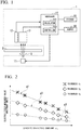
- Fig. 1 is a diagram showing an example of a configuration of a measurement device 1 according to the present embodiment.
- the measurement device 1 includes an electric field generation source 11, a thickness gauge 12, a sensor 13, a processor 14, a storage 15, and an output 16.
- the processor 14 includes a calculator 141 and a controller 142.
- the measurement device 1 measures a thickness and an electric field value of a sample 2 (a measurement target) and obtains a specific dielectric constant of the sample 2 on the basis of measured values.
- the sample 2 (the measurement target) is a film- or sheet-shaped dielectric.
- the sample 2 is inserted between the electric field generation source 11 (an electric field generator) and the sensor 13 (an electric field detector).
- the electric field generation source 11 generates an AC electric field 3 in accordance with control of the controller 142 of the processor 14.
- the thickness gauge 12 is a sensor that measures a thickness of the sample 2 in, for example, an optical type, an ultrasonic type, or the like.
- the thickness gauge 12 measures the thickness of the sample 2 in a non-contact manner and outputs a measured value to the calculator 141 of the processor 14.
- the thickness gauge 12 is disposed so that the thickness gauge 12 is not in contact with the sample 2.
- the sensor 13 detects the AC electric field 3 generated by the electric field generation source 11 and outputs an electric field measured value (an intensity of the AC electric field) according to an intensity of a frequency component to the calculator 141.
- the sensor 13 detects the intensity of the AC electric field 3 attenuated by the sample 2.
- the sensor 13 detects the intensity of the AC electric field 3 in a state in which the sample 2 is absent.
- the sensor 13 may be an electric field sensor such as an electro-optic probe (see Non-Patent Literature 1) using an electro-optic crystal having an electro-optic effect.
- the electric field generation source 11 and the sensor 13 are disposed to face each other.
- the electric field generation source 11 and the sensor 13 are disposed at a distance from each other so that the electric field generation source 11 and the sensor 13 as not in contact with the sample 2 (the measurement target).
- the distance is, for example, several tens of micrometers ( ⁇ m) to several millimeters (mm).
- the calculator 141 obtains the specific dielectric constant of the sample 2 using the detection value output from the thickness gauge 12, the electric field measured value output from the sensor 13, and information stored in the storage 15. The calculator 141 outputs the obtained specific dielectric constant to the output 16. A method of obtaining the specific dielectric constant will be described later.
- the controller 142 controls the start and end of the electric field generation of the electric field generation source 11 and a magnitude of the electric field.
- the storage 15 stores a relationship (a calibration curve) between the specific dielectric constant and the electric field measured value for each thickness of the sample.
- the storage 15 stores information indicating a relationship between the thickness of the sample and a slope of a graph representing a relationship between the specific dielectric constant and the electric field measured value. Further, the storage 15 stores information representing a relationship between the thickness of the sample and an intercept of the graph representing the relationship between the specific dielectric constant and the electric field measured value. Further, the storage 15 stores information representing a relationship between the thickness of the sample and the electric field measurement value.
- the output 16 is, for example, a display device, a printing device, or the like.
- the output 16 displays or prints the specific dielectric constant output from the calculator 141.
- Fig. 2 is a diagram showing an example of a calibration curve between a specific dielectric constant and an electric field measured value according to the present embodiment.
- the horizontal axis represents a specific dielectric constant and the vertical axis represents an electric field measured value (an arbitrary unit).
- the reference sign g1 represents a relationship between the specific dielectric constant and the electric field measured value when a thickness of a sample is t 1 .
- a cross mark represents results of measuring electric field measured values in samples having different specific dielectric constants at the thickness of t 1 .
- the reference sign g2 represents a relationship between the specific dielectric constant and the electric field measured value when the thickness of the sample is t 2 .
- a diamond mark represents results of measuring electric field measured values in samples having different specific dielectric constants at the thickness of t 2 .
- the reference sign g3 represents a relationship between the specific dielectric constant and the electric field measured value when the thickness of the sample is t 3 .
- a circle mark represents results of measuring electric field measured values in samples having different specific dielectric constants at the thickness of t 3 .
- the intensity of the AC electric field 3 detected by the sensor 13 decreases in a proportional relationship because electrical conductivity (corresponding to a dielectric loss in a dielectric) proportional to an imaginary part correlated with a real part of a complex dielectric constant increases and a loss is caused in accordance with a Kramers-Kronig relation equation. Because there is such a relationship between the specific dielectric constant and the electric field measured value, the specific dielectric constant and the electric field measured value are represented by a linear function by performing linear approximation according to regression analysis in the present embodiment.
- Fig. 3 is a flowchart of the procedure of introducing the calibration curve according to the present embodiment.
- the following process is performed using a sample whose thickness and specific dielectric constant are known before the sample 2 whose specific dielectric constant is desired to be obtained is measured.
- sample 1 (a specific dielectric constant ⁇ r1 ), sample 2 (a specific dielectric constant ⁇ r2 ), ..., and sample m (a specific dielectric constant ⁇ rm ) which have a thickness t 1 , ...
- sample 1 (a specific dielectric constant ⁇ r1 ), sample 2 (a specific dielectric constant ⁇ r2 ), ..., and sample m (a specific dielectric constant ⁇ rm ) which have a thickness t n are used.
- the number of samples used in the pre-process is n ⁇ m.
- the thickness of the sample may be unknown.
- the measurement device 1 measures the thickness of the sample with the thickness gauge 12.
- Each sample may be a sheet- or film-shaped general plastic material having a stable specific dielectric constant. It is desirable that n and m are 3 or more so that an approximation process is performed.
- the calculator 141 iterates loop processing L2s to L2e and the processing of step S2 n times. In the processing of the first iteration, the calculator 141 sets i to 0 and adds 1 to i. The calculator 141 adds 1 to i in the processing of second and subsequent iterations.
- the calculator 141 iterates the processing of step S1 m times.
- the calculator 141 sets j to 0 and adds 1 to j.
- the calculator 141 adds 1 to j in the processing of second and subsequent iterations.
- Step S1 An operator places a sample (a general material) having a thickness of t i and a specific dielectric constant of ⁇ j between the electric field generation source 11 ( Fig. 1 ) and the sensor 13 ( Fig. 1 ).
- the calculator 141 acquires an electric field measured value V ij of the sample.
- Step S2 The calculator 141 obtains a calibration curve A of the electric field measured value with respect to the specific dielectric constant according to linear approximation for each thickness t i . Subsequently, the calculator 141 causes the storage 15 to store a slope a and an intercept b of the calibration curve A.
- the measurement device 1 measures an electric field measured value V 11 of a first sample (a specific dielectric constant ⁇ r1 ) having a thickness t 1 .
- the measurement device 1 measures an electric field measured value V 12 of a second sample (a specific dielectric constant ⁇ r2 ) having the thickness t 1 .
- the measurement device 1 measures an electric field measured value V 13 of a third sample (a specific dielectric constant ⁇ r3 ) having the thickness t 1 (loop processing L2s to L2e of a first iteration).
- the calculator 141 causes the storage 15 to store a slope a 1 and an intercept b 1 of the calibration curve A 1 .
- the measurement device 1 measures an electric field measured value V 24 of a fourth sample (a specific dielectric constant ⁇ r4 ) having a thickness t 2 .
- the measurement device 1 measures an electric field measured value V 25 of a fifth sample (a specific dielectric constant ⁇ r5 ) having the thickness t 2 .
- the measurement device 1 measures an electric field measured value V 26 of a sixth sample (a specific dielectric constant ⁇ r6 ) having the thickness t 2 (loop processing L2s to L2e of a second iteration).
- the calculator 141 causes the storage 15 to store a slope a 2 and an intercept b 2 of the calibration curve A 2 .
- the measurement device 1 measures an electric field measured value V 37 of a seventh sample (a specific dielectric constant ⁇ r7 ) having a thickness t 3 .
- the measurement device 1 measures an electric field measured value V 38 of an eighth sample (a specific dielectric constant ⁇ r8 ) having the thickness t 3 .
- the measurement device 1 measures an electric field measured value V 39 of a ninth sample (a specific dielectric constant ⁇ r9 ) having the thickness t 3 (loop processing L2s to L2e of a third iteration).
- the calculator 141 causes the storage 15 to store a slope a 3 and an intercept b 3 of the calibration curve A 3 .
- Fig. 2 Measurement results obtained by the above-described process are as shown in Fig. 2 .
- the example of Fig. 2 is an example in which a pre-process is performed using 21 samples.
- a graph when the electric field measured value V is taken on the vertical axis and the thickness t is taken on the horizontal axis is shown as Fig. 4.
- Fig. 4 will be described below.
- the calculator 141 obtains a function using, for example, exponential approximation.
- Fig. 4 is a diagram showing an example of the relationship between the thickness and the electric field measured value.
- the horizontal axis represents the thickness ( ⁇ m) and the vertical axis represents an electric field measured value (an arbitrary unit).
- the intensity of the AC electric field 3 detected by the sensor 13 exponentially decreases as shown in Fig. 4 because a passage loss occurs in accordance with the Lambert-Beer law.
- the electric field measured value is V
- the attenuation coefficient is c
- the electric field measured value which is the intensity of the AC electric field 3 detected by the sensor 13 is a function of the thickness and the specific dielectric constant of the sample 2 which is a measurement target. Therefore, when either the thickness or the specific dielectric constant is desired to be obtained, the other value can be obtained from either one value thereof and the electric field measured value. Because the purpose of the present embodiment is to measure the specific dielectric constant, the thickness of the sample 2 is acquired by the thickness gauge 12 together with the electric field measured value.
- Fig. 5 is a flowchart of a procedure of measuring the specific dielectric constant according to the present embodiment.
- the sample 2 whose specific dielectric constant is to be measured in Fig. 5 is a dielectric material whose specific dielectric constant and thickness are unknown.
- the operator places the sample 2 between the electric field generation source 11 ( Fig. 1 ) and the sensor 13 ( Fig. 1 ).
- Step S11 The calculator 141 acquires a measured value of a thickness t x of the sample 2 output from the thickness gauge 12.
- Step S12 The calculator 141 acquires an electric field measured value V x of the sample 2 output from the sensor 13.
- Fig. 6 is a block diagram of an example of a configuration of an electro-optic probe 13A.
- Fig. 6 shows an example in which the electro-optic probe 13A is applied to the sensor 13.
- the electro-optic probe 13A includes an EO/OE circuit 131 and a probe head 132.
- the EO/OE circuit 131 includes an LD driver 1311, an LD 1312, a PD 1313, a PD 1314, a differential amplifier 1315, and a capacitor 1316.
- the probe head 132 includes a wave plate 1321, an EO crystal 1322, and a PBS 1323.
- the EO/OE circuit 131 converts an electric field intensity detected by the probe head 132 into an electrical signal and outputs the electrical signal.
- the LD driver 1311 drives the LD 1312.
- the LD 1312 is, for example, a semiconductor laser.
- the PD 1313 and the PD 1314 are light receivers, receive P waves and S waves of laser light from the probe head 132, convert the received P and S waves into electrical signals, and output the electrical signals to the differential amplifier 1315.
- the differential amplifier 1315 obtains a difference between the electrical signal output by the PD 1313 and the electrical signal output by the PD 1314 and outputs an output signal obtained by amplifying an obtained intensity difference and cutting a direct current (DC) component by the capacitor 1316.
- DC direct current
- Laser light radiated by the LD 1312 of the EO/OE circuit 131 is transmitted to the probe head 132 via an optical fiber.
- the laser light transmitted through the wave plate 1321 and the EO crystal 1322 is split into two linearly polarized light beams of P and S waves by the PBS 1323 (a polarizing beam splitter).
- the EO crystal 1322 is a crystal exhibiting an electro-optic (EO) effect in which a refractive index of the crystal changes when an electric field is applied to the crystal.
- EO electro-optic
- the configuration of the electro-optic probe 13A shown in Fig. 6 is an example, and the configuration is not limited thereto.
- the measurement device 1 of the present embodiment can be used to implement the non-contact measurement of a specific dielectric constant, which was not possible in the conventional technology.
- an electro-optic probe for the sensor 13 that detects the electric field can be employed to perform stable measurement with low disturbance as compared with measurement using a metal antenna.
- a frequency of a signal input to the electric field generation source 11 is about several kHz to several MHz, so that it is possible to achieve an effect that the device can be cost-effectively constructed as compared with a measurement method using a millimeter wave band or a microwave band without the need for speeding up the signal detection circuit.
- the measurement device 1 is applied during a process in which a sheet- or film-shaped dielectric material is conveyed and manufactured at a high speed.
- in-line measurement of the specific dielectric constant can be implemented with high spatial resolution in a non-contact manner.
- Fig. 7 is a diagram showing an example in which the measurement device 1 of the present embodiment is applied to a manufacturing device 100 by which a sheet- or film-shaped dielectric material is conveyed and manufactured at a high speed.
- the manufacturing device 100 includes a measurement device 1 and a conveyance means 101 (a conveyance device).
- a conveyance means 101 a conveyance device.
- the x-axis is in a direction along a conveyance direction D1 of the sample 2
- the y-axis is in a direction along a width direction of the sample 2
- the z-axis is in a direction along a vertical direction.
- the sample 2 is conveyed at a high speed in the x-axis direction by a conveyance means 101 such as an aluminum roll for winding and conveying the sample 2.
- a conveyance means 101 such as an aluminum roll for winding and conveying the sample 2.
- S/N deterioration can be restricted by exciting the electric field generation source 11 with a high-voltage AC signal and increasing the intensity of the AC electric field 3 detected by the sensor 13. It is easy to generate a high-voltage signal in a relatively low frequency band.
- the relatively low frequency is, for example, about several kHz to several MHz.
- a high-voltage signal of about several kHz to several MHz is used, so that high-precision measurement can be easily implemented even if the distance between the sensor 13 and the electric field generation source 11 is increased.
- the sample 2 When the distance between the sample 2 and the sensor 13 or the distance between the sample 2 and the electric field generation source 11 is as short as in the conventional technology, the sample 2 is in contact with the sensor 13 and the electric field generation source 11 and hence problems such as scratches and holes on the surface of the sample 2 occur.
- the sample 2 is conveyed in a state in which a gap having a sufficient distance is secured, so that contact does not occur and high-precision measurement can be performed as described above.
- Fig. 8 is a perspective view showing a schematic configuration of a measurement device 1A according to the present embodiment. As shown in Fig. 8 , the measurement device 1A further includes a frame 10.
- the frame 10 is a substantially square ring-shaped member having a longitudinal direction and a short direction as external shapes.
- the frame 10 supports the thickness gauge 12, the sensor 13, and the electric field generation source 11 so that they can reciprocate in the longitudinal direction within an opening OP of the frame 10.
- the frame 10 is disposed so that the longitudinal direction is in a width direction (a y-direction) of the paper P, the short direction is in a vertical direction (a z-direction), and the sample 2 passes through substantially the center of the opening OP.
- the frame 10 is aligned with respect to the sample 2 so that the thickness gauge 12 and the sensor 13 are disposed above the sample 2 to be conveyed and the electric field generation source 11 is disposed below the sample 2 to be conveyed.
- a mechanism for causing the thickness gauge 12 and the sensor 13 to reciprocate in the y-direction along the front surface of the sample 2 and a mechanism for causing the electric field generation source 11 to reciprocate in the y-direction along the back surface of the sample 2 are provided. That is, the measurement device 1A has a scanning mechanism (a movement device) in a horizontal direction orthogonal to a conveying direction of the sample 2 (a measurement target). If these mechanisms are driven in the same manner, the thickness gauge 12, the sensor 13, and the electric field generation source 11 can be reciprocated in synchronization with each other.
- All or part of processing to be performed by the processor 14 may be performed by recording a program for implementing all or some of the functions of the processor 14 according to the present invention on a computer-readable recording medium and causing a computer system to read and execute the program recorded on the recording medium.
- the "computer system” used here is assumed to include an operating system (OS) and hardware such as peripheral devices.
- the "computer system” is assumed to include a homepage providing environment (or displaying environment) when a World Wide Web (WWW) system is used.
- the "computer-readable recording medium” refers to a storage device, including a portable medium such as a flexible disk, a magneto-optical disc, a read only memory (ROM), and a compact disc (CD)-ROM, and a hard disk embedded in the computer system.
- the "computer-readable recording medium” is assumed to include a computer-readable recording medium for retaining the program for a predetermined time period as in a volatile memory (a random access memory (RAM)) inside the computer system including a server and a client when the program is transmitted via a network such as the Internet or a communication circuit such as a telephone circuit.
- a volatile memory a random access memory (RAM)
- RAM random access memory
- the above-described program may be transmitted from a computer system storing the program in a storage device or the like via a transmission medium or by transmission waves in a transmission medium to another computer system.
- the "transmission medium” for transmitting the program refers to a medium having a function of transmitting information, such as a network (a communication network) like the Internet or a communication circuit (a communication line) like a telephone circuit.
- the above-described program may be a program for implementing some of the above-described functions. Further, the above-described program may be a program capable of implementing the above-described function in combination with a program already recorded on the computer system, i.e., a so-called differential file (differential program).
Landscapes
- Physics & Mathematics (AREA)
- General Physics & Mathematics (AREA)
- Electromagnetism (AREA)
- Measurement Of Resistance Or Impedance (AREA)
- Measurement Of Length, Angles, Or The Like Using Electric Or Magnetic Means (AREA)
Applications Claiming Priority (2)
| Application Number | Priority Date | Filing Date | Title |
|---|---|---|---|
| JP2018180874A JP7113427B2 (ja) | 2018-09-26 | 2018-09-26 | 測定装置、および測定方法 |
| PCT/JP2019/036732 WO2020066828A1 (ja) | 2018-09-26 | 2019-09-19 | 測定装置、および測定方法 |
Publications (3)
| Publication Number | Publication Date |
|---|---|
| EP3859355A1 true EP3859355A1 (de) | 2021-08-04 |
| EP3859355A4 EP3859355A4 (de) | 2022-07-06 |
| EP3859355B1 EP3859355B1 (de) | 2023-11-01 |
Family
ID=69952048
Family Applications (1)
| Application Number | Title | Priority Date | Filing Date |
|---|---|---|---|
| EP19865218.2A Active EP3859355B1 (de) | 2018-09-26 | 2019-09-19 | Messvorrichtung und messverfahren |
Country Status (4)
| Country | Link |
|---|---|
| US (1) | US12174231B2 (de) |
| EP (1) | EP3859355B1 (de) |
| JP (1) | JP7113427B2 (de) |
| WO (1) | WO2020066828A1 (de) |
Cited By (1)
| Publication number | Priority date | Publication date | Assignee | Title |
|---|---|---|---|---|
| CN115808578A (zh) * | 2022-12-02 | 2023-03-17 | 南方电网数字电网研究院有限公司 | 电力设备的电压获取方法、装置、设备、存储介质 |
Families Citing this family (4)
| Publication number | Priority date | Publication date | Assignee | Title |
|---|---|---|---|---|
| JP7739806B2 (ja) * | 2021-07-19 | 2025-09-17 | 横河電機株式会社 | 電界センサ |
| CN114460379B (zh) * | 2021-12-31 | 2025-01-17 | 武汉轻工大学 | 电场监测系统及方法 |
| CN114487562B (zh) * | 2022-04-06 | 2022-07-05 | 南方电网数字电网研究院有限公司 | 基于校正介电常数的电压测量方法和装置 |
| CN119437123A (zh) * | 2025-01-08 | 2025-02-14 | 宁德时代新能源科技股份有限公司 | 测量方法和测量系统 |
Family Cites Families (18)
| Publication number | Priority date | Publication date | Assignee | Title |
|---|---|---|---|---|
| JPS61182582A (ja) * | 1985-02-08 | 1986-08-15 | Murata Mfg Co Ltd | 誘電体板の比誘電率測定方法および測定器具 |
| FR2685490B1 (fr) | 1991-12-19 | 1996-05-15 | Commissariat Energie Atomique | Dispositif de mesure de parametres dielectriques et magnetiques de materiaux et systeme de mesure desdits parametres utilisant ce dispositif. |
| US5309110A (en) * | 1992-03-04 | 1994-05-03 | The Perkin Elmer Corporation | Differential dielectric analyzer |
| JP3289398B2 (ja) * | 1993-05-19 | 2002-06-04 | 株式会社村田製作所 | 誘電体板の比誘電率測定方法および測定器具 |
| JP3204852B2 (ja) * | 1994-09-02 | 2001-09-04 | 株式会社村田製作所 | 非線形誘電率測定装置 |
| EP1116951A4 (de) * | 1998-09-25 | 2003-05-14 | Oji Paper Co | Verfahren und vorrichtung zur messung der dielektrizitätskonstante |
| JP2000162158A (ja) | 1998-09-25 | 2000-06-16 | Oji Paper Co Ltd | 誘電率測定方法及び装置 |
| DE19937387C1 (de) * | 1999-08-07 | 2001-03-01 | Itw Ind Gmbh | Vorrichtung zur Überwachung eines Auftrags eines flüssigen bis pastenförmigen Mediums auf ein Substrat |
| US6809533B1 (en) * | 1999-09-10 | 2004-10-26 | University Of Maryland, College Park | Quantitative imaging of dielectric permittivity and tunability |
| JP3823073B2 (ja) * | 2002-06-21 | 2006-09-20 | 株式会社日立ハイテクノロジーズ | 電子線を用いた検査方法及び検査装置 |
| JP3660997B2 (ja) * | 2002-11-26 | 2005-06-15 | 独立行政法人情報通信研究機構 | 3次元電界分布測定方法および3次元電界分布測定装置 |
| US7285963B2 (en) * | 2004-04-09 | 2007-10-23 | Solid State Measurements, Inc. | Method and system for measurement of dielectric constant of thin films using a near field microwave probe |
| JP2006349425A (ja) * | 2005-06-14 | 2006-12-28 | Oji Paper Co Ltd | 坪量測定方法及び装置 |
| JP4906386B2 (ja) * | 2006-03-30 | 2012-03-28 | 横河電機株式会社 | プロファイル制御方法及びその装置 |
| JP4819663B2 (ja) | 2006-12-13 | 2011-11-24 | 株式会社エヌ・ティ・ティ・ドコモ | 複素誘電率測定装置及び複素誘電率測定方法 |
| JP2009229423A (ja) | 2008-03-25 | 2009-10-08 | Kobe Steel Ltd | 近接場プローブ及びこの近接場プローブを備えた電気的特性測定装置 |
| JP5295047B2 (ja) | 2009-09-03 | 2013-09-18 | 株式会社日立ハイテクサイエンス | 走査型プローブ顕微鏡による誘電率の測定方法 |
| JP6961987B2 (ja) | 2017-04-12 | 2021-11-05 | 富士通株式会社 | 日時情報抽出方法、日時情報抽出装置及び日時情報抽出プログラム |
-
2018
- 2018-09-26 JP JP2018180874A patent/JP7113427B2/ja active Active
-
2019
- 2019-09-19 EP EP19865218.2A patent/EP3859355B1/de active Active
- 2019-09-19 WO PCT/JP2019/036732 patent/WO2020066828A1/ja not_active Ceased
- 2019-09-19 US US17/275,743 patent/US12174231B2/en active Active
Cited By (2)
| Publication number | Priority date | Publication date | Assignee | Title |
|---|---|---|---|---|
| CN115808578A (zh) * | 2022-12-02 | 2023-03-17 | 南方电网数字电网研究院有限公司 | 电力设备的电压获取方法、装置、设备、存储介质 |
| CN115808578B (zh) * | 2022-12-02 | 2023-12-12 | 南方电网数字电网研究院有限公司 | 电力设备的电压获取方法、装置、设备、存储介质 |
Also Published As
| Publication number | Publication date |
|---|---|
| WO2020066828A1 (ja) | 2020-04-02 |
| EP3859355B1 (de) | 2023-11-01 |
| US12174231B2 (en) | 2024-12-24 |
| JP7113427B2 (ja) | 2022-08-05 |
| US20220034951A1 (en) | 2022-02-03 |
| JP2020051870A (ja) | 2020-04-02 |
| EP3859355A4 (de) | 2022-07-06 |
Similar Documents
| Publication | Publication Date | Title |
|---|---|---|
| EP3859355B1 (de) | Messvorrichtung und messverfahren | |
| US11009340B2 (en) | Film thickness measuring method and film thickness measuring apparatus | |
| US20170023469A1 (en) | System for determining at least one property of a sheet dielectric sample using terahertz radiation | |
| CN100388008C (zh) | 比吸收率测量系统和方法 | |
| KR101788450B1 (ko) | 테라헤르츠파를 이용한 투명 박막의 두께를 측정하는 장치 및 그 측정 방법 | |
| CN104568249B (zh) | 一种基于太赫兹时域光谱系统的应力测量方法 | |
| CN102192884B (zh) | 利用偏振可控的太赫兹波对样品进行成像的方法 | |
| US9645045B2 (en) | SHG imaging technique for assessing hybrid EO polymer/silicon photonic integrated circuits | |
| JPS63307329A (ja) | 単一モード光フアイバにおける偏り及び複屈折を測定する方法 | |
| CN102680119B (zh) | 一种激光器频率稳定度的测量方法和装置 | |
| CN105928606A (zh) | 一种声表面波光干涉扫描探测系统 | |
| CN106370727B (zh) | 基于应力波波场检测波速、材料状态及损伤程度的方法 | |
| Kimbrough | In-line roll-to-roll metrology for flexible electronics | |
| Kukotenko et al. | Approaches to the study of the evanescent field of terahertz surface plasmon polaritons at the Novosibirsk free electron laser | |
| Gut et al. | Determination of the attenuation of planar waveguides by means of detecting scattered light | |
| Mattei et al. | Leaky wave detection at air–solid interfaces by laser interferometry | |
| US7317517B2 (en) | Birefringence profiler | |
| Karmarkar et al. | An analytical model to evaluate the volumetric strain in a polymeric material using terahertz time-domain spectroscopy | |
| KR100945387B1 (ko) | 시료의 비선형계수의 균질성 검사 장치 | |
| Zhu et al. | Two-dimensional optical measurement techniques based on optical birefringence effects | |
| Salzenstein et al. | Brillouin light scattering uncertainty preliminary estimation | |
| Salzenstein | Uncertainty estimation in optics and optoelectronic systems | |
| Wang et al. | Method for detecting blasting beads in cigarette filter | |
| Le et al. | Acoustic transmission across the interface in impulsive stimulated Brillouin microscopy | |
| Whitaker et al. | Slab coupled optical fiber sensor calibration |
Legal Events
| Date | Code | Title | Description |
|---|---|---|---|
| STAA | Information on the status of an ep patent application or granted ep patent |
Free format text: STATUS: THE INTERNATIONAL PUBLICATION HAS BEEN MADE |
|
| PUAI | Public reference made under article 153(3) epc to a published international application that has entered the european phase |
Free format text: ORIGINAL CODE: 0009012 |
|
| STAA | Information on the status of an ep patent application or granted ep patent |
Free format text: STATUS: REQUEST FOR EXAMINATION WAS MADE |
|
| 17P | Request for examination filed |
Effective date: 20210317 |
|
| AK | Designated contracting states |
Kind code of ref document: A1 Designated state(s): AL AT BE BG CH CY CZ DE DK EE ES FI FR GB GR HR HU IE IS IT LI LT LU LV MC MK MT NL NO PL PT RO RS SE SI SK SM TR |
|
| DAV | Request for validation of the european patent (deleted) | ||
| DAX | Request for extension of the european patent (deleted) | ||
| A4 | Supplementary search report drawn up and despatched |
Effective date: 20220603 |
|
| RIC1 | Information provided on ipc code assigned before grant |
Ipc: G01R 29/12 20060101ALI20220530BHEP Ipc: G01N 27/00 20060101ALI20220530BHEP Ipc: G01R 27/26 20060101AFI20220530BHEP |
|
| GRAP | Despatch of communication of intention to grant a patent |
Free format text: ORIGINAL CODE: EPIDOSNIGR1 |
|
| STAA | Information on the status of an ep patent application or granted ep patent |
Free format text: STATUS: GRANT OF PATENT IS INTENDED |
|
| RIN1 | Information on inventor provided before grant (corrected) |
Inventor name: SHINAGAWA, MITSURU Inventor name: MATSUMOTO, YOSHINORI Inventor name: KATSUYAMA, JUN |
|
| INTG | Intention to grant announced |
Effective date: 20230503 |
|
| GRAS | Grant fee paid |
Free format text: ORIGINAL CODE: EPIDOSNIGR3 |
|
| GRAA | (expected) grant |
Free format text: ORIGINAL CODE: 0009210 |
|
| STAA | Information on the status of an ep patent application or granted ep patent |
Free format text: STATUS: THE PATENT HAS BEEN GRANTED |
|
| AK | Designated contracting states |
Kind code of ref document: B1 Designated state(s): AL AT BE BG CH CY CZ DE DK EE ES FI FR GB GR HR HU IE IS IT LI LT LU LV MC MK MT NL NO PL PT RO RS SE SI SK SM TR |
|
| REG | Reference to a national code |
Ref country code: GB Ref legal event code: FG4D |
|
| REG | Reference to a national code |
Ref country code: CH Ref legal event code: EP |
|
| REG | Reference to a national code |
Ref country code: DE Ref legal event code: R096 Ref document number: 602019040793 Country of ref document: DE |
|
| REG | Reference to a national code |
Ref country code: IE Ref legal event code: FG4D |
|
| RAP4 | Party data changed (patent owner data changed or rights of a patent transferred) |
Owner name: HOSEI UNIVERSITY Owner name: YOKOGAWA ELECTRIC CORPORATION |
|
| P01 | Opt-out of the competence of the unified patent court (upc) registered |
Effective date: 20240112 |
|
| REG | Reference to a national code |
Ref country code: LT Ref legal event code: MG9D |
|
| REG | Reference to a national code |
Ref country code: NL Ref legal event code: MP Effective date: 20231101 |
|
| PG25 | Lapsed in a contracting state [announced via postgrant information from national office to epo] |
Ref country code: GR Free format text: LAPSE BECAUSE OF FAILURE TO SUBMIT A TRANSLATION OF THE DESCRIPTION OR TO PAY THE FEE WITHIN THE PRESCRIBED TIME-LIMIT Effective date: 20240202 |
|
| PG25 | Lapsed in a contracting state [announced via postgrant information from national office to epo] |
Ref country code: IS Free format text: LAPSE BECAUSE OF FAILURE TO SUBMIT A TRANSLATION OF THE DESCRIPTION OR TO PAY THE FEE WITHIN THE PRESCRIBED TIME-LIMIT Effective date: 20240301 |
|
| PG25 | Lapsed in a contracting state [announced via postgrant information from national office to epo] |
Ref country code: LT Free format text: LAPSE BECAUSE OF FAILURE TO SUBMIT A TRANSLATION OF THE DESCRIPTION OR TO PAY THE FEE WITHIN THE PRESCRIBED TIME-LIMIT Effective date: 20231101 |
|
| REG | Reference to a national code |
Ref country code: AT Ref legal event code: MK05 Ref document number: 1627797 Country of ref document: AT Kind code of ref document: T Effective date: 20231101 |
|
| PG25 | Lapsed in a contracting state [announced via postgrant information from national office to epo] |
Ref country code: NL Free format text: LAPSE BECAUSE OF FAILURE TO SUBMIT A TRANSLATION OF THE DESCRIPTION OR TO PAY THE FEE WITHIN THE PRESCRIBED TIME-LIMIT Effective date: 20231101 |
|
| PG25 | Lapsed in a contracting state [announced via postgrant information from national office to epo] |
Ref country code: AT Free format text: LAPSE BECAUSE OF FAILURE TO SUBMIT A TRANSLATION OF THE DESCRIPTION OR TO PAY THE FEE WITHIN THE PRESCRIBED TIME-LIMIT Effective date: 20231101 |
|
| PG25 | Lapsed in a contracting state [announced via postgrant information from national office to epo] |
Ref country code: ES Free format text: LAPSE BECAUSE OF FAILURE TO SUBMIT A TRANSLATION OF THE DESCRIPTION OR TO PAY THE FEE WITHIN THE PRESCRIBED TIME-LIMIT Effective date: 20231101 |
|
| PG25 | Lapsed in a contracting state [announced via postgrant information from national office to epo] |
Ref country code: NL Free format text: LAPSE BECAUSE OF FAILURE TO SUBMIT A TRANSLATION OF THE DESCRIPTION OR TO PAY THE FEE WITHIN THE PRESCRIBED TIME-LIMIT Effective date: 20231101 Ref country code: LT Free format text: LAPSE BECAUSE OF FAILURE TO SUBMIT A TRANSLATION OF THE DESCRIPTION OR TO PAY THE FEE WITHIN THE PRESCRIBED TIME-LIMIT Effective date: 20231101 Ref country code: IS Free format text: LAPSE BECAUSE OF FAILURE TO SUBMIT A TRANSLATION OF THE DESCRIPTION OR TO PAY THE FEE WITHIN THE PRESCRIBED TIME-LIMIT Effective date: 20240301 Ref country code: GR Free format text: LAPSE BECAUSE OF FAILURE TO SUBMIT A TRANSLATION OF THE DESCRIPTION OR TO PAY THE FEE WITHIN THE PRESCRIBED TIME-LIMIT Effective date: 20240202 Ref country code: ES Free format text: LAPSE BECAUSE OF FAILURE TO SUBMIT A TRANSLATION OF THE DESCRIPTION OR TO PAY THE FEE WITHIN THE PRESCRIBED TIME-LIMIT Effective date: 20231101 Ref country code: BG Free format text: LAPSE BECAUSE OF FAILURE TO SUBMIT A TRANSLATION OF THE DESCRIPTION OR TO PAY THE FEE WITHIN THE PRESCRIBED TIME-LIMIT Effective date: 20240201 Ref country code: AT Free format text: LAPSE BECAUSE OF FAILURE TO SUBMIT A TRANSLATION OF THE DESCRIPTION OR TO PAY THE FEE WITHIN THE PRESCRIBED TIME-LIMIT Effective date: 20231101 Ref country code: PT Free format text: LAPSE BECAUSE OF FAILURE TO SUBMIT A TRANSLATION OF THE DESCRIPTION OR TO PAY THE FEE WITHIN THE PRESCRIBED TIME-LIMIT Effective date: 20240301 |
|
| PG25 | Lapsed in a contracting state [announced via postgrant information from national office to epo] |
Ref country code: SE Free format text: LAPSE BECAUSE OF FAILURE TO SUBMIT A TRANSLATION OF THE DESCRIPTION OR TO PAY THE FEE WITHIN THE PRESCRIBED TIME-LIMIT Effective date: 20231101 Ref country code: RS Free format text: LAPSE BECAUSE OF FAILURE TO SUBMIT A TRANSLATION OF THE DESCRIPTION OR TO PAY THE FEE WITHIN THE PRESCRIBED TIME-LIMIT Effective date: 20231101 Ref country code: PL Free format text: LAPSE BECAUSE OF FAILURE TO SUBMIT A TRANSLATION OF THE DESCRIPTION OR TO PAY THE FEE WITHIN THE PRESCRIBED TIME-LIMIT Effective date: 20231101 Ref country code: NO Free format text: LAPSE BECAUSE OF FAILURE TO SUBMIT A TRANSLATION OF THE DESCRIPTION OR TO PAY THE FEE WITHIN THE PRESCRIBED TIME-LIMIT Effective date: 20240201 Ref country code: LV Free format text: LAPSE BECAUSE OF FAILURE TO SUBMIT A TRANSLATION OF THE DESCRIPTION OR TO PAY THE FEE WITHIN THE PRESCRIBED TIME-LIMIT Effective date: 20231101 Ref country code: HR Free format text: LAPSE BECAUSE OF FAILURE TO SUBMIT A TRANSLATION OF THE DESCRIPTION OR TO PAY THE FEE WITHIN THE PRESCRIBED TIME-LIMIT Effective date: 20231101 |
|
| PG25 | Lapsed in a contracting state [announced via postgrant information from national office to epo] |
Ref country code: DK Free format text: LAPSE BECAUSE OF FAILURE TO SUBMIT A TRANSLATION OF THE DESCRIPTION OR TO PAY THE FEE WITHIN THE PRESCRIBED TIME-LIMIT Effective date: 20231101 |
|
| PG25 | Lapsed in a contracting state [announced via postgrant information from national office to epo] |
Ref country code: CZ Free format text: LAPSE BECAUSE OF FAILURE TO SUBMIT A TRANSLATION OF THE DESCRIPTION OR TO PAY THE FEE WITHIN THE PRESCRIBED TIME-LIMIT Effective date: 20231101 |
|
| PG25 | Lapsed in a contracting state [announced via postgrant information from national office to epo] |
Ref country code: SK Free format text: LAPSE BECAUSE OF FAILURE TO SUBMIT A TRANSLATION OF THE DESCRIPTION OR TO PAY THE FEE WITHIN THE PRESCRIBED TIME-LIMIT Effective date: 20231101 |
|
| PG25 | Lapsed in a contracting state [announced via postgrant information from national office to epo] |
Ref country code: SM Free format text: LAPSE BECAUSE OF FAILURE TO SUBMIT A TRANSLATION OF THE DESCRIPTION OR TO PAY THE FEE WITHIN THE PRESCRIBED TIME-LIMIT Effective date: 20231101 Ref country code: SK Free format text: LAPSE BECAUSE OF FAILURE TO SUBMIT A TRANSLATION OF THE DESCRIPTION OR TO PAY THE FEE WITHIN THE PRESCRIBED TIME-LIMIT Effective date: 20231101 Ref country code: IT Free format text: LAPSE BECAUSE OF FAILURE TO SUBMIT A TRANSLATION OF THE DESCRIPTION OR TO PAY THE FEE WITHIN THE PRESCRIBED TIME-LIMIT Effective date: 20231101 Ref country code: EE Free format text: LAPSE BECAUSE OF FAILURE TO SUBMIT A TRANSLATION OF THE DESCRIPTION OR TO PAY THE FEE WITHIN THE PRESCRIBED TIME-LIMIT Effective date: 20231101 Ref country code: DK Free format text: LAPSE BECAUSE OF FAILURE TO SUBMIT A TRANSLATION OF THE DESCRIPTION OR TO PAY THE FEE WITHIN THE PRESCRIBED TIME-LIMIT Effective date: 20231101 Ref country code: CZ Free format text: LAPSE BECAUSE OF FAILURE TO SUBMIT A TRANSLATION OF THE DESCRIPTION OR TO PAY THE FEE WITHIN THE PRESCRIBED TIME-LIMIT Effective date: 20231101 |
|
| REG | Reference to a national code |
Ref country code: DE Ref legal event code: R097 Ref document number: 602019040793 Country of ref document: DE |
|
| PLBE | No opposition filed within time limit |
Free format text: ORIGINAL CODE: 0009261 |
|
| STAA | Information on the status of an ep patent application or granted ep patent |
Free format text: STATUS: NO OPPOSITION FILED WITHIN TIME LIMIT |
|
| 26N | No opposition filed |
Effective date: 20240802 |
|
| PG25 | Lapsed in a contracting state [announced via postgrant information from national office to epo] |
Ref country code: SI Free format text: LAPSE BECAUSE OF FAILURE TO SUBMIT A TRANSLATION OF THE DESCRIPTION OR TO PAY THE FEE WITHIN THE PRESCRIBED TIME-LIMIT Effective date: 20231101 |
|
| PG25 | Lapsed in a contracting state [announced via postgrant information from national office to epo] |
Ref country code: SI Free format text: LAPSE BECAUSE OF FAILURE TO SUBMIT A TRANSLATION OF THE DESCRIPTION OR TO PAY THE FEE WITHIN THE PRESCRIBED TIME-LIMIT Effective date: 20231101 |
|
| PG25 | Lapsed in a contracting state [announced via postgrant information from national office to epo] |
Ref country code: MC Free format text: LAPSE BECAUSE OF FAILURE TO SUBMIT A TRANSLATION OF THE DESCRIPTION OR TO PAY THE FEE WITHIN THE PRESCRIBED TIME-LIMIT Effective date: 20231101 |
|
| REG | Reference to a national code |
Ref country code: CH Ref legal event code: PL |
|
| PG25 | Lapsed in a contracting state [announced via postgrant information from national office to epo] |
Ref country code: LU Free format text: LAPSE BECAUSE OF NON-PAYMENT OF DUE FEES Effective date: 20240919 |
|
| REG | Reference to a national code |
Ref country code: BE Ref legal event code: MM Effective date: 20240930 |
|
| PG25 | Lapsed in a contracting state [announced via postgrant information from national office to epo] |
Ref country code: BE Free format text: LAPSE BECAUSE OF NON-PAYMENT OF DUE FEES Effective date: 20240930 |
|
| PG25 | Lapsed in a contracting state [announced via postgrant information from national office to epo] |
Ref country code: CH Free format text: LAPSE BECAUSE OF NON-PAYMENT OF DUE FEES Effective date: 20240930 |
|
| PG25 | Lapsed in a contracting state [announced via postgrant information from national office to epo] |
Ref country code: IE Free format text: LAPSE BECAUSE OF NON-PAYMENT OF DUE FEES Effective date: 20240919 |
|
| PG25 | Lapsed in a contracting state [announced via postgrant information from national office to epo] |
Ref country code: FI Free format text: LAPSE BECAUSE OF FAILURE TO SUBMIT A TRANSLATION OF THE DESCRIPTION OR TO PAY THE FEE WITHIN THE PRESCRIBED TIME-LIMIT Effective date: 20231101 |
|
| PGFP | Annual fee paid to national office [announced via postgrant information from national office to epo] |
Ref country code: DE Payment date: 20250923 Year of fee payment: 7 |
|
| PGFP | Annual fee paid to national office [announced via postgrant information from national office to epo] |
Ref country code: GB Payment date: 20250927 Year of fee payment: 7 |
|
| PGFP | Annual fee paid to national office [announced via postgrant information from national office to epo] |
Ref country code: FR Payment date: 20250926 Year of fee payment: 7 |
|
| PG25 | Lapsed in a contracting state [announced via postgrant information from national office to epo] |
Ref country code: RO Free format text: LAPSE BECAUSE OF FAILURE TO SUBMIT A TRANSLATION OF THE DESCRIPTION OR TO PAY THE FEE WITHIN THE PRESCRIBED TIME-LIMIT Effective date: 20231101 |
|
| PG25 | Lapsed in a contracting state [announced via postgrant information from national office to epo] |
Ref country code: CY Free format text: LAPSE BECAUSE OF FAILURE TO SUBMIT A TRANSLATION OF THE DESCRIPTION OR TO PAY THE FEE WITHIN THE PRESCRIBED TIME-LIMIT; INVALID AB INITIO Effective date: 20190919 |
|
| PG25 | Lapsed in a contracting state [announced via postgrant information from national office to epo] |
Ref country code: HU Free format text: LAPSE BECAUSE OF FAILURE TO SUBMIT A TRANSLATION OF THE DESCRIPTION OR TO PAY THE FEE WITHIN THE PRESCRIBED TIME-LIMIT; INVALID AB INITIO Effective date: 20190919 |