EP3859965A1 - Perfectionnements apportés ou se rapportant à des modules en mailles de chaîne pour convertisseurs de source de tension - Google Patents
Perfectionnements apportés ou se rapportant à des modules en mailles de chaîne pour convertisseurs de source de tension Download PDFInfo
- Publication number
- EP3859965A1 EP3859965A1 EP20275020.4A EP20275020A EP3859965A1 EP 3859965 A1 EP3859965 A1 EP 3859965A1 EP 20275020 A EP20275020 A EP 20275020A EP 3859965 A1 EP3859965 A1 EP 3859965A1
- Authority
- EP
- European Patent Office
- Prior art keywords
- chain
- link
- energy storage
- switching elements
- link module
- Prior art date
- Legal status (The legal status is an assumption and is not a legal conclusion. Google has not performed a legal analysis and makes no representation as to the accuracy of the status listed.)
- Granted
Links
Images


Classifications
-
- H—ELECTRICITY
- H02—GENERATION; CONVERSION OR DISTRIBUTION OF ELECTRIC POWER
- H02M—APPARATUS FOR CONVERSION BETWEEN AC AND AC, BETWEEN AC AND DC, OR BETWEEN DC AND DC, AND FOR USE WITH MAINS OR SIMILAR POWER SUPPLY SYSTEMS; CONVERSION OF DC OR AC INPUT POWER INTO SURGE OUTPUT POWER; CONTROL OR REGULATION THEREOF
- H02M1/00—Details of apparatus for conversion
- H02M1/32—Means for protecting converters other than automatic disconnection
-
- H—ELECTRICITY
- H02—GENERATION; CONVERSION OR DISTRIBUTION OF ELECTRIC POWER
- H02M—APPARATUS FOR CONVERSION BETWEEN AC AND AC, BETWEEN AC AND DC, OR BETWEEN DC AND DC, AND FOR USE WITH MAINS OR SIMILAR POWER SUPPLY SYSTEMS; CONVERSION OF DC OR AC INPUT POWER INTO SURGE OUTPUT POWER; CONTROL OR REGULATION THEREOF
- H02M7/00—Conversion of AC power input into DC power output; Conversion of DC power input into AC power output
- H02M7/42—Conversion of DC power input into AC power output without possibility of reversal
- H02M7/44—Conversion of DC power input into AC power output without possibility of reversal by static converters
- H02M7/48—Conversion of DC power input into AC power output without possibility of reversal by static converters using discharge tubes with control electrode or semiconductor devices with control electrode
- H02M7/483—Converters with outputs that each can have more than two voltages levels
- H02M7/4835—Converters with outputs that each can have more than two voltages levels comprising two or more cells, each including a switchable capacitor, the capacitors having a nominal charge voltage which corresponds to a given fraction of the input voltage, and the capacitors being selectively connected in series to determine the instantaneous output voltage
-
- H—ELECTRICITY
- H02—GENERATION; CONVERSION OR DISTRIBUTION OF ELECTRIC POWER
- H02M—APPARATUS FOR CONVERSION BETWEEN AC AND AC, BETWEEN AC AND DC, OR BETWEEN DC AND DC, AND FOR USE WITH MAINS OR SIMILAR POWER SUPPLY SYSTEMS; CONVERSION OF DC OR AC INPUT POWER INTO SURGE OUTPUT POWER; CONTROL OR REGULATION THEREOF
- H02M1/00—Details of apparatus for conversion
- H02M1/32—Means for protecting converters other than automatic disconnection
- H02M1/322—Means for rapidly discharging a capacitor of the converter for protecting electrical components or for preventing electrical shock
Definitions
- This invention relates to a chain-link module, for connection in series with other chain-link modules to form a chain-link converter selectively operable to provide a stepped variable voltage source within a voltage source converter, and to such a voltage source converter.
- AC power is typically converted to DC power for transmission via overhead lines, under-sea cables and/or underground cables. This conversion removes the need to compensate for the AC capacitive load effects imposed by the power transmission medium, i.e. the transmission line or cable, and reduces the cost per kilometre of the lines and/or cables, and thus becomes cost-effective when power needs to be transmitted over a long distance.
- DC power is also transmitted directly from offshore wind parks to onshore AC power transmission networks.
- converters i.e. power converters
- One type of power converter is a voltage source converter, although other types of power converter are also possible.
- Such a voltage source converter includes first and second DC terminals between which extends at least one converter limb, and typically three converter limbs each of which corresponds to a given phase of a three-phase electrical power system.
- the or each converter limb includes first and second limb portions which are separated by an AC terminal.
- the first and second DC terminals are connected to a DC network, and the or each AC terminal is connected to a corresponding phase of an AC network.
- Each limb portion includes a chain-link converter which extends between the associated AC terminal and a corresponding one of the first or the second DC terminal.
- Each chain-link converter includes a plurality of series connected chain-link modules, while each chain-link module includes a number of switching elements which are connected in parallel with an energy storage device, usually in the form of a capacitor.
- an energy storage device usually in the form of a capacitor.
- Other types of energy storage device i.e. any device that is capable of storing and releasing energy to selectively provide a voltage, e.g. a fuel cell or battery, may also be used however.
- the provision of a plurality of chain-link modules means that it is possible to build up a combined voltage across each chain-link converter, via the insertion of the energy storage devices, i.e. the capacitors, of multiple chain-link modules (with each chain-link module providing its own voltage), which is higher than the voltage available from each individual chain-link module.
- each of the chain-link modules work together to permit the chain-link converter to provide a stepped variable voltage source. This permits the generation of a voltage waveform across each chain-link converter using a step-wise approximation. As such each chain-link converter is capable of providing a wide range of complex waveforms.
- each chain-link converter in the foregoing manner can be used to generate an AC voltage waveform at the or each AC terminal, and thereby enable the voltage source converter to provide the aforementioned power transfer functionality between the AC and DC networks.
- a chain-link module for connection in series with other chain-link modules to form a chain-link converter selectively operable to provide a stepped variable voltage source within a voltage source converter, the chain-link module comprising:
- Having a chain-link module that is able to provide a positive voltage is desirable because it allows a chain-link converter within which the module is located to generate a regular voltage of the type that is needed for normal power transmission by an associated voltage source converter. Such a positive voltage can also be used to oppose a fault current flowing from the first connection terminal to the second connection terminal.
- arranging the second pair of series-connected switching elements in parallel with only one of the energy storage devices, and separating them with the second connection terminal means that when such a positive voltage is being provided (i.e. during normal power transmission by an associated voltage source converter) current can be directed through both energy storage devices, as required, via only two switching elements.
- arranging the second pair of switching elements in the aforementioned manner permits the use of selective switching of those switching elements, while the chain-link module is otherwise providing a positive voltage during normal power transmission, to alter the ratio of energy stored by each of the first and second energy storage devices.
- selective switching of the switching elements may be used to re-balance the energy stored by each energy storage device, which is desirable in some operating circumstances.
- the ability of the chain-link module to selectively provide a negative voltage is advantageous because it can be used to oppose a DC fault current flowing through the chain-link module from the second connection terminal to the first connection terminal and so, in conjunction with the aforementioned positive voltage capability, enables a chain-link converter within which the module is, in use, located (and hence also an associated voltage source converter including such a chain-link converter) to provide full DC fault clearing functionality, i.e. the ability to clear DC fault currents flowing in either direction between the first and second connection terminals.
- full DC fault clearing functionality i.e. the ability to clear DC fault currents flowing in either direction between the first and second connection terminals.
- a further benefit is that such DC fault clearing functionality can be provided using a plurality of identical chain-link modules of the invention within an associated chain-link converter. This simplifies the manufacture and subsequent control of such a chain-link converter compared to, e.g. a chain-link converter incorporating chain-link modules that differ from one another.
- first and second chain-link converters (having one or more chain-link modules of the invention therein) to work together in a converter limb of an associated voltage source converter to over-modulate, i.e. generate a positive converter limb voltage which is greater than the DC operating voltage of a corresponding DC network with which the voltage source converter is connected, or generate a negative converter limb voltage.
- At least one of the energy storage devices has a selectively operable rapid discharge circuit connected therewith.
- the energy stored by the said one of the first and second energy storage devices (with which the second pair of switching elements are connected in parallel) will rise transiently as a result of inductive energy being stored as the fault current is suppressed, and the triggering, i.e. selective operation, of a rapid discharge circuit connected with the said storage device affected by the additional inductive energy, can be used to reduce the amount of energy stored.
- each energy storage device has a selectively operable rapid discharge circuit connected therewith.
- each energy storage device with a rapid discharge circuit allows the energy stored by each energy storage device to be reduced, as mentioned hereinabove.
- each energy storage device having a rapid discharge circuit also permits the relative ratio of energy stored by the first and second energy storage devices to be altered, e.g. to re-balance the energy so stored.
- At least one of the switching elements in the second pair of switching elements has a lower voltage rating than one or both of the switching elements in the first pair of switching elements.
- the positive voltage provided by the chain-link module has a first magnitude that is commensurate with the combined energy stored by the first and second energy storage devices, whereas the negative voltage provided has a second magnitude which is commensurate with only the energy stored by the said one of the first and second energy storage devices with which the second pair of switching elements is connected in parallel.
- the second magnitude is therefore lower than the first magnitude, and so the voltage that must be supported by the second pair of switching elements is also lower than that which has to be supported by the first pair of switching elements.
- the chain-link module may further include a module controller programmed to cause the first and second energy storage devices to store different amounts of energy.
- first and second energy storage devices store different amounts of energy advantageously allows for a tuning of an associated DC fault clearing functionality.
- having the energy storage device connected in parallel with the second pair of switching elements store more energy than the other energy storage device means that the negative voltage provided by the chain-link module is larger than would be the case if both energy storage devices stored the same amount of energy.
- a consequence of being able to provide such a larger negative voltage is that it achieves more rapid DC fault clearing.
- a voltage source converter comprising at least one chain-link converter having a plurality of series-connected chain link modules, at least one of the said chain-link modules being a chain-link module as described hereinabove.
- the voltage source converter of the invention shares the benefits of the corresponding features of the chain-link module of the invention.
- first and second in this patent specification is merely intended to help distinguish between similar features (e.g. the first and second series-connected energy storage devices), and is not intended to indicate the relative importance of one feature over another feature, unless otherwise specified.
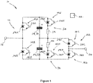
- a chain-link module according to a first embodiment of the invention is designated generally by reference numeral 10.
- the chain-link module 10 includes a first pair 12 of series-conducted switching elements, i.e. series-connected first and second switching elements 14A, 14B, that are separated by a first connection terminal 16, and which are also connected in parallel with first and second series-connected energy storage devices 18, 20.
- the chain-link module 10 also includes a second pair 22 of series-connected switching elements, i.e. series-connected third and fourth switching elements 14C, 14D, which are separated by a second connection terminal 24.
- the second pair 22 of switching elements 14C, 14D is connected in parallel with only one of the first and second energy storage devices 18, 20.
- this is the second energy storage device 20, although in other embodiments of the invention (not shown) the second pair of switching elements may instead be connected in parallel with only the first energy storage device.
- the first switching element 14A includes a first semiconductor device, in the form of a first IGBT 26A, which is connected in parallel with a first anti-parallel diode 28A.
- the second, third and fourth switching elements 14B, 14C, 14D similarly include corresponding second, third and fourth IGBTs 26B, 26C, 26D that are connected in parallel with a corresponding second, third or fourth anti-parallel diode 28B, 28C, 28D.
- each switching element 14A, 14B, 14C, 14D can be considered an active switching element because it can be turned on and off, at will, by a control signal.
- a passive current check element alone, which instead requires a biasing voltage to be applied across its conduction terminals in order to cause it to allow or block the flow of current therethrough. It is not always possible to provide such a biasing voltage, and so such passive elements cannot be turned on and off at will.
- each of the switching elements 14A, 14B, 14C, 14D shares the same configuration in that each includes an IGBT 26A, 26B, 26C, 26D arranged in parallel with a corresponding anti-parallel diode 28A, 28B, 28C, 28D, although this need not necessarily be the case in other embodiments of the invention.
- one or more other types of self-commutated semiconductor devices such as a gate turn-off thyristor (GTO), a field effect transistor (FET), a metal-oxide-semiconductor field-effect transistor (MOSFET), an injection-enhanced gate transistor (IEGT), an integrated gate commutated thyristor (IGCT), a bimode insulated gate transistor (BIGT) or any other self-commutated switching device instead of an IGBT.
- one or more of the semiconductor devices may instead include a wide-bandgap material such as, but not limited to, silicon carbide, boron nitride, gallium nitride and aluminium nitride.
- the number of semiconductor devices in each switching element 14A, 14B, 14C, 14D may vary depending on the required voltage and current ratings of that switching element 14A, 14B, 14C, 14D.
- Alternative passive current check elements i.e. alternatives to the anti-parallel diodes 28A, 28B, 28C, 28D may also be included in other embodiments of the invention, e.g. any alternative element that is capable of limiting current flow in only one direction.
- the number of passive current check elements in each switching element 14A, 14B, 14C, 14D may vary too depending on the required voltage and current ratings of that switching element 14A, 14B, 14C, 14D.
- each of the switching elements in the second pair 20 of switching elements i.e. each of the third and fourth switching elements 14C, 14D
- each of the first and second switching elements 14A, 14B may be rated at 6.5 kV, while the third and fourth switching elements 14C, 14D may be less expensive and less lossy 3.3 kV rated switching elements.
- first and second energy storage devices 18, 20 take the form of corresponding first and second capacitors 30, 32, although other types of energy storage device, i.e. other types of device capable of storing and releasing energy to selectively provide a voltage, e.g. a fuel cell or battery, may be used.
- each energy storage device 18, 20, i.e. each of the first and second capacitors 30, 32 has a corresponding first or second selectively operable rapid discharge circuit 34, 36 connected therewith, and more particularly connected in parallel therewith.
- the first rapid discharge circuit 34 is formed from a further, fifth switching element 14E comprising a fifth IGBT 26E connected in parallel with a fifth anti-parallel diode 28E, which in turn is connected in series with an energy dissipating element in the form of a first resistor 38.
- the second rapid discharge circuit 36 similarly is formed from a sixth switching element 14F, comprising a sixth IGBT 26F connected in parallel with a sixth anti-parallel diode 28F, arranged in series with a second resistor 40.
- the fifth and sixth switching elements 14E, 14F may have the same rating as the third and fourth switching elements 14C, 14D, e.g. 3.3 kV, although this need not necessarily be the case.
- the fifth and sixth switching elements and anti-parallel diodes 14E, 14F, 28E, 28F may also differ in the same manner as described hereinabove, and other forms of energy dissipating element may also be used in other embodiments of the invention (not shown).
- the first to fourth switching elements 14A, 14B, 14C, 14D are selectively switched, e.g. by a module controller 42 programmed to control such switching, in order to direct current I through the chain-link module 10 along different current flow paths in order to cause the chain-link module 10 to provide a positive, zero and negative voltage.
- switching on of the first and fourth switching elements 14A, 14D i.e. switching on of the corresponding first and fourth IGBTs 26A, 26D therein, directs current I in a first direction 44 through the chain-link module 10 from the second connection terminal 24 to the first connection terminal 16 and through both of the first and second energy storage devices 18, 20, i.e. through both of the first and second capacitors 30, 32, as shown schematically in Figure 2(a) .
- This causes the chain-link module 10 to provide a positive voltage with a first magnitude which is commensurate with the combined energy, i.e. equal to the sum of the voltages, stored by the first and second capacitors 30, 32.
- Such a positive voltage contributes towards the provision of a regular voltage by a chain-link converter within which the chain-link module 10 is, in use, included, and thereby facilitates normal power transfer by an associated voltage source converter within which the said chain-link converter is, in turn, incorporated.
- such a positive voltage can be used to oppose, and subsequently extinguish, a DC fault current I F flowing in a second direction 46, opposite the first direction 44, through the chain-link module 10 from the first connection terminal 16 to the second connection terminal 24.
- switching on of the second and third switching elements 14B, 14C directs current I in the second direction 46 through the chain-link module 10, i.e. from the first terminal 16 to the second terminal 24, and through only the second capacitor 32, as shown schematically in Figure 2(d) .
- This causes the chain-link module to provide a negative voltage with a second magnitude that is commensurate with the energy stored by only the second capacitor 32, i.e. equal to the voltage stored by only the second capacitor 32.
- Such a negative voltage can, nevertheless, still be used to oppose, and subsequently extinguish, a DC fault current I F flowing in the first direction 44 through the chain-link module 10 from the second terminal 24 to the first terminal 16.
- the first and second capacitors 30, 32 i.e. the first and second energy storage devices 18, 20 store the same amount of energy, i.e. are charged to the same voltage
- the first magnitude of the positive voltage is double the second magnitude of the negative voltage.
- the first magnitude of the positive voltage is not exactly double the second magnitude of the negative voltage.
- the first capacitor 30 may be controlled to store a voltage of 1.8 kV, while the second capacitor 32 is controlled to store a larger voltage of 2.2 kV.
- the first magnitude of the positive voltage will remain as the sum of the voltages stored by the first and second capacitors 30, 32, e.g. 4.0 kV, while the second magnitude of the negative voltage will be more than half of the positive voltage, i.e. will be equal to the voltage stored by the second capacitor 32, e.g. will be 2.2 kV.
- the third switching element 14C i.e. the third IGBT 26C therein, may be switched on to direct current I to flow in the second direction 46 from the first connection terminal 16, through the first anti-parallel diode 28, through only the first capacitor 30 and, through the said third IGBT 26C to the second connection terminal 24.
- the first switching element 14A i.e. the first IGBT 26A therein, may be switched on to directing current I to flow in the first direction 44 from the second connection terminal 24, through the third anti-parallel diode 28C, through only the first capacitor 30 and, through the said first IGBT 26A to the first connection terminal.
- Directing current I to flow through only the first capacitor 30 in either of the foregoing manners, may be used for a short duration to adjust the ratio of energies stored by the first and second capacitors 30, 32.
- one or other, or both, of the rapid discharge circuits 34, 36 may be triggered, i.e. by turning on the IGBT 26E, 26F in the corresponding fifth or sixth switching element 14E, 14F to remove energy, i.e. voltage, from the energy storage device 18, 20, i.e. capacitor 30, 32 with which it is connected.
- a voltage source converter (not shown) comprises at least one chain-link converter having a plurality of series-connected chain-link modules, at least one of the said chain-link modules being a chain-link module 10, as described hereinabove.
Landscapes
- Engineering & Computer Science (AREA)
- Power Engineering (AREA)
- Dc-Dc Converters (AREA)
- Charge And Discharge Circuits For Batteries Or The Like (AREA)
Priority Applications (4)
| Application Number | Priority Date | Filing Date | Title |
|---|---|---|---|
| EP20275020.4A EP3859965B1 (fr) | 2020-01-30 | 2020-01-30 | Perfectionnements apportés ou se rapportant à des modules en mailles de chaîne pour convertisseurs de source de tension |
| US17/795,683 US12027993B2 (en) | 2020-01-30 | 2021-01-25 | Chain-link modules for voltage source converters |
| CN202180011752.6A CN114982120B (zh) | 2020-01-30 | 2021-01-25 | 用于电压源转换器的链式链路模块中或与其相关的改进 |
| PCT/EP2021/051575 WO2021151819A1 (fr) | 2020-01-30 | 2021-01-25 | Améliorations apportées à des modules à maillons de chaîne pour convertisseurs de source de tension |
Applications Claiming Priority (1)
| Application Number | Priority Date | Filing Date | Title |
|---|---|---|---|
| EP20275020.4A EP3859965B1 (fr) | 2020-01-30 | 2020-01-30 | Perfectionnements apportés ou se rapportant à des modules en mailles de chaîne pour convertisseurs de source de tension |
Publications (2)
| Publication Number | Publication Date |
|---|---|
| EP3859965A1 true EP3859965A1 (fr) | 2021-08-04 |
| EP3859965B1 EP3859965B1 (fr) | 2023-09-06 |
Family
ID=69423242
Family Applications (1)
| Application Number | Title | Priority Date | Filing Date |
|---|---|---|---|
| EP20275020.4A Active EP3859965B1 (fr) | 2020-01-30 | 2020-01-30 | Perfectionnements apportés ou se rapportant à des modules en mailles de chaîne pour convertisseurs de source de tension |
Country Status (4)
| Country | Link |
|---|---|
| US (1) | US12027993B2 (fr) |
| EP (1) | EP3859965B1 (fr) |
| CN (1) | CN114982120B (fr) |
| WO (1) | WO2021151819A1 (fr) |
Families Citing this family (1)
| Publication number | Priority date | Publication date | Assignee | Title |
|---|---|---|---|---|
| CN118316298A (zh) * | 2024-06-05 | 2024-07-09 | 东北林业大学 | 一种具备直流故障穿越与能量耗散功能的mmc子模块 |
Citations (5)
| Publication number | Priority date | Publication date | Assignee | Title |
|---|---|---|---|---|
| CN101051751A (zh) * | 2007-05-14 | 2007-10-10 | 上海艾帕电力电子有限公司 | 含有功率单元的有源电力滤波器及其控制方法 |
| CN106998151A (zh) * | 2017-04-21 | 2017-08-01 | 上海交通大学 | 基于不对称双子模块和半桥子模块的多电平换流器 |
| EP3373438A1 (fr) * | 2015-11-03 | 2018-09-12 | Hyosung Corporation | Dispositif de décharge de condensateur à l'intérieur d'un sous-module de convertisseur modulaire multiniveaux (mmc) |
| CN109120174A (zh) * | 2018-09-03 | 2019-01-01 | 国网山东省电力公司潍坊供电公司 | 基于双子mmc模块的电容电压均衡方法 |
| CN106877718B (zh) * | 2017-04-21 | 2019-04-05 | 上海交通大学 | 模块化多电平换流器不对称双子模块中点电位均衡控制方法 |
Family Cites Families (9)
| Publication number | Priority date | Publication date | Assignee | Title |
|---|---|---|---|---|
| EP2650999A3 (fr) | 2010-04-08 | 2015-11-04 | Alstom Technology Ltd | Convertisseur de source de tension à multi module pour une liaison à haute tension continue |
| EP2782239A1 (fr) * | 2013-03-21 | 2014-09-24 | Alstom Technology Ltd | Convertisseur électronique de puissance |
| EP2852040A1 (fr) * | 2013-09-20 | 2015-03-25 | Alstom Technology Ltd | Module |
| EP2852019B8 (fr) | 2013-09-23 | 2020-10-21 | General Electric Technology GmbH | Améliorations apportées ou relatives aux modules de puissance destinés à être utilisés dans des réseaux de transmission de puissance |
| US10069430B2 (en) * | 2013-11-07 | 2018-09-04 | Regents Of The University Of Minnesota | Modular converter with multilevel submodules |
| EP3662572A1 (fr) * | 2017-09-28 | 2020-06-10 | Siemens Aktiengesellschaft | Sous-module conçu pour un convertisseur modulaire multiniveaux |
| CN208241593U (zh) * | 2018-01-11 | 2018-12-14 | Abb瑞士股份有限公司 | 电压源变流器 |
| EP3544163B1 (fr) * | 2018-03-21 | 2020-09-16 | General Electric Technology GmbH | Convertisseur |
| EP3547525A1 (fr) * | 2018-03-27 | 2019-10-02 | General Electric Technology GmbH | Appareil convertisseur de source de tension |
-
2020
- 2020-01-30 EP EP20275020.4A patent/EP3859965B1/fr active Active
-
2021
- 2021-01-25 WO PCT/EP2021/051575 patent/WO2021151819A1/fr not_active Ceased
- 2021-01-25 CN CN202180011752.6A patent/CN114982120B/zh active Active
- 2021-01-25 US US17/795,683 patent/US12027993B2/en active Active
Patent Citations (5)
| Publication number | Priority date | Publication date | Assignee | Title |
|---|---|---|---|---|
| CN101051751A (zh) * | 2007-05-14 | 2007-10-10 | 上海艾帕电力电子有限公司 | 含有功率单元的有源电力滤波器及其控制方法 |
| EP3373438A1 (fr) * | 2015-11-03 | 2018-09-12 | Hyosung Corporation | Dispositif de décharge de condensateur à l'intérieur d'un sous-module de convertisseur modulaire multiniveaux (mmc) |
| CN106998151A (zh) * | 2017-04-21 | 2017-08-01 | 上海交通大学 | 基于不对称双子模块和半桥子模块的多电平换流器 |
| CN106877718B (zh) * | 2017-04-21 | 2019-04-05 | 上海交通大学 | 模块化多电平换流器不对称双子模块中点电位均衡控制方法 |
| CN109120174A (zh) * | 2018-09-03 | 2019-01-01 | 国网山东省电力公司潍坊供电公司 | 基于双子mmc模块的电容电压均衡方法 |
Non-Patent Citations (3)
| Title |
|---|
| ADAM GRAIN PHILIP ET AL: "New Efficient Submodule for a Modular Multilevel Converter in Multiterminal HVDC Networks", IEEE TRANSACTIONS ON POWER ELECTRONICS, INSTITUTE OF ELECTRICAL AND ELECTRONICS ENGINEERS, USA, vol. 32, no. 6, 1 June 2017 (2017-06-01), pages 4258 - 4278, XP011640902, ISSN: 0885-8993, [retrieved on 20170210], DOI: 10.1109/TPEL.2016.2603180 * |
| LU MAOZENG ET AL: "Imbalance Mechanism and Balanced Control of Capacitor Voltage for a Hybrid Modular Multilevel Converter", IEEE TRANSACTIONS ON POWER ELECTRONICS, INSTITUTE OF ELECTRICAL AND ELECTRONICS ENGINEERS, USA, vol. 33, no. 7, 1 July 2018 (2018-07-01), pages 5686 - 5696, XP011679873, ISSN: 0885-8993, [retrieved on 20180319], DOI: 10.1109/TPEL.2017.2743780 * |
| NAMI ALIREZA ET AL: "Modular Multilevel Converters for HVDC Applications: Review on Converter Cells and Functionalities", IEEE TRANSACTIONS ON POWER ELECTRONICS, INSTITUTE OF ELECTRICAL AND ELECTRONICS ENGINEERS, USA, vol. 30, no. 1, 1 January 2015 (2015-01-01), pages 18 - 36, XP011557523, ISSN: 0885-8993, [retrieved on 20140826], DOI: 10.1109/TPEL.2014.2327641 * |
Also Published As
| Publication number | Publication date |
|---|---|
| EP3859965B1 (fr) | 2023-09-06 |
| WO2021151819A1 (fr) | 2021-08-05 |
| US12027993B2 (en) | 2024-07-02 |
| CN114982120B (zh) | 2026-02-03 |
| US20230119315A1 (en) | 2023-04-20 |
| CN114982120A (zh) | 2022-08-30 |
Similar Documents
| Publication | Publication Date | Title |
|---|---|---|
| US11777401B2 (en) | Fault tolerant AC-DC chain-link converter | |
| EP2586112A1 (fr) | Convertisseur multi-niveaux en cascade pour application hvdc | |
| US20170264187A1 (en) | A voltage source converter | |
| US20160164296A1 (en) | Module | |
| WO2018100051A1 (fr) | Perfectionnements apportés ou se rapportant à des convertisseurs de secteur ccht | |
| US20210359617A1 (en) | Electrical assembly | |
| WO2015036457A1 (fr) | Convertisseur de source de tension | |
| US12027993B2 (en) | Chain-link modules for voltage source converters | |
| EP2849330A1 (fr) | Convertisseur modulaire à plusieurs niveaux et module | |
| WO2015039942A1 (fr) | Module | |
| “Lisa” Qi et al. | ABB’s recent advances in solid-state circuit breakers | |
| US12341345B2 (en) | Converter stations | |
| US11721978B2 (en) | Switching valve | |
| US12003169B2 (en) | Chain-link modules for voltage source converters | |
| US20240055865A1 (en) | Controller for power electronic device | |
| WO2021198381A1 (fr) | Améliorations dans ou associées à des convertisseurs à cellules reliés en chaîne | |
| US12143028B2 (en) | Electrical assembly | |
| EP3930171A1 (fr) | Module | |
| US20230402935A1 (en) | Electrical assembly | |
| EP3972102A1 (fr) | Améliorations apportées ou se rapportant à des schémas de transmission de puissance |
Legal Events
| Date | Code | Title | Description |
|---|---|---|---|
| PUAI | Public reference made under article 153(3) epc to a published international application that has entered the european phase |
Free format text: ORIGINAL CODE: 0009012 |
|
| STAA | Information on the status of an ep patent application or granted ep patent |
Free format text: STATUS: THE APPLICATION HAS BEEN PUBLISHED |
|
| AK | Designated contracting states |
Kind code of ref document: A1 Designated state(s): AL AT BE BG CH CY CZ DE DK EE ES FI FR GB GR HR HU IE IS IT LI LT LU LV MC MK MT NL NO PL PT RO RS SE SI SK SM TR |
|
| RAP3 | Party data changed (applicant data changed or rights of an application transferred) |
Owner name: GENERAL ELECTRIC TECHNOLOGY GMBH |
|
| STAA | Information on the status of an ep patent application or granted ep patent |
Free format text: STATUS: REQUEST FOR EXAMINATION WAS MADE |
|
| 17P | Request for examination filed |
Effective date: 20220201 |
|
| RBV | Designated contracting states (corrected) |
Designated state(s): AL AT BE BG CH CY CZ DE DK EE ES FI FR GB GR HR HU IE IS IT LI LT LU LV MC MK MT NL NO PL PT RO RS SE SI SK SM TR |
|
| GRAP | Despatch of communication of intention to grant a patent |
Free format text: ORIGINAL CODE: EPIDOSNIGR1 |
|
| STAA | Information on the status of an ep patent application or granted ep patent |
Free format text: STATUS: GRANT OF PATENT IS INTENDED |
|
| INTG | Intention to grant announced |
Effective date: 20220610 |
|
| GRAJ | Information related to disapproval of communication of intention to grant by the applicant or resumption of examination proceedings by the epo deleted |
Free format text: ORIGINAL CODE: EPIDOSDIGR1 |
|
| STAA | Information on the status of an ep patent application or granted ep patent |
Free format text: STATUS: REQUEST FOR EXAMINATION WAS MADE |
|
| INTC | Intention to grant announced (deleted) | ||
| GRAP | Despatch of communication of intention to grant a patent |
Free format text: ORIGINAL CODE: EPIDOSNIGR1 |
|
| STAA | Information on the status of an ep patent application or granted ep patent |
Free format text: STATUS: GRANT OF PATENT IS INTENDED |
|
| INTG | Intention to grant announced |
Effective date: 20230404 |
|
| P01 | Opt-out of the competence of the unified patent court (upc) registered |
Effective date: 20230522 |
|
| GRAS | Grant fee paid |
Free format text: ORIGINAL CODE: EPIDOSNIGR3 |
|
| GRAA | (expected) grant |
Free format text: ORIGINAL CODE: 0009210 |
|
| STAA | Information on the status of an ep patent application or granted ep patent |
Free format text: STATUS: THE PATENT HAS BEEN GRANTED |
|
| AK | Designated contracting states |
Kind code of ref document: B1 Designated state(s): AL AT BE BG CH CY CZ DE DK EE ES FI FR GB GR HR HU IE IS IT LI LT LU LV MC MK MT NL NO PL PT RO RS SE SI SK SM TR |
|
| REG | Reference to a national code |
Ref country code: GB Ref legal event code: FG4D |
|
| REG | Reference to a national code |
Ref country code: CH Ref legal event code: EP |
|
| REG | Reference to a national code |
Ref country code: DE Ref legal event code: R096 Ref document number: 602020017171 Country of ref document: DE |
|
| REG | Reference to a national code |
Ref country code: IE Ref legal event code: FG4D |
|
| REG | Reference to a national code |
Ref country code: SE Ref legal event code: TRGR |
|
| REG | Reference to a national code |
Ref country code: LT Ref legal event code: MG9D |
|
| REG | Reference to a national code |
Ref country code: NL Ref legal event code: MP Effective date: 20230906 |
|
| PG25 | Lapsed in a contracting state [announced via postgrant information from national office to epo] |
Ref country code: GR Free format text: LAPSE BECAUSE OF FAILURE TO SUBMIT A TRANSLATION OF THE DESCRIPTION OR TO PAY THE FEE WITHIN THE PRESCRIBED TIME-LIMIT Effective date: 20231207 |
|
| PG25 | Lapsed in a contracting state [announced via postgrant information from national office to epo] |
Ref country code: RS Free format text: LAPSE BECAUSE OF FAILURE TO SUBMIT A TRANSLATION OF THE DESCRIPTION OR TO PAY THE FEE WITHIN THE PRESCRIBED TIME-LIMIT Effective date: 20230906 Ref country code: NO Free format text: LAPSE BECAUSE OF FAILURE TO SUBMIT A TRANSLATION OF THE DESCRIPTION OR TO PAY THE FEE WITHIN THE PRESCRIBED TIME-LIMIT Effective date: 20231206 Ref country code: LV Free format text: LAPSE BECAUSE OF FAILURE TO SUBMIT A TRANSLATION OF THE DESCRIPTION OR TO PAY THE FEE WITHIN THE PRESCRIBED TIME-LIMIT Effective date: 20230906 Ref country code: LT Free format text: LAPSE BECAUSE OF FAILURE TO SUBMIT A TRANSLATION OF THE DESCRIPTION OR TO PAY THE FEE WITHIN THE PRESCRIBED TIME-LIMIT Effective date: 20230906 Ref country code: HR Free format text: LAPSE BECAUSE OF FAILURE TO SUBMIT A TRANSLATION OF THE DESCRIPTION OR TO PAY THE FEE WITHIN THE PRESCRIBED TIME-LIMIT Effective date: 20230906 Ref country code: GR Free format text: LAPSE BECAUSE OF FAILURE TO SUBMIT A TRANSLATION OF THE DESCRIPTION OR TO PAY THE FEE WITHIN THE PRESCRIBED TIME-LIMIT Effective date: 20231207 Ref country code: FI Free format text: LAPSE BECAUSE OF FAILURE TO SUBMIT A TRANSLATION OF THE DESCRIPTION OR TO PAY THE FEE WITHIN THE PRESCRIBED TIME-LIMIT Effective date: 20230906 |
|
| REG | Reference to a national code |
Ref country code: AT Ref legal event code: MK05 Ref document number: 1609835 Country of ref document: AT Kind code of ref document: T Effective date: 20230906 |
|
| PG25 | Lapsed in a contracting state [announced via postgrant information from national office to epo] |
Ref country code: NL Free format text: LAPSE BECAUSE OF FAILURE TO SUBMIT A TRANSLATION OF THE DESCRIPTION OR TO PAY THE FEE WITHIN THE PRESCRIBED TIME-LIMIT Effective date: 20230906 |
|
| PG25 | Lapsed in a contracting state [announced via postgrant information from national office to epo] |
Ref country code: IS Free format text: LAPSE BECAUSE OF FAILURE TO SUBMIT A TRANSLATION OF THE DESCRIPTION OR TO PAY THE FEE WITHIN THE PRESCRIBED TIME-LIMIT Effective date: 20240106 |
|
| PG25 | Lapsed in a contracting state [announced via postgrant information from national office to epo] |
Ref country code: AT Free format text: LAPSE BECAUSE OF FAILURE TO SUBMIT A TRANSLATION OF THE DESCRIPTION OR TO PAY THE FEE WITHIN THE PRESCRIBED TIME-LIMIT Effective date: 20230906 |
|
| PG25 | Lapsed in a contracting state [announced via postgrant information from national office to epo] |
Ref country code: ES Free format text: LAPSE BECAUSE OF FAILURE TO SUBMIT A TRANSLATION OF THE DESCRIPTION OR TO PAY THE FEE WITHIN THE PRESCRIBED TIME-LIMIT Effective date: 20230906 |
|
| PG25 | Lapsed in a contracting state [announced via postgrant information from national office to epo] |
Ref country code: SM Free format text: LAPSE BECAUSE OF FAILURE TO SUBMIT A TRANSLATION OF THE DESCRIPTION OR TO PAY THE FEE WITHIN THE PRESCRIBED TIME-LIMIT Effective date: 20230906 Ref country code: RO Free format text: LAPSE BECAUSE OF FAILURE TO SUBMIT A TRANSLATION OF THE DESCRIPTION OR TO PAY THE FEE WITHIN THE PRESCRIBED TIME-LIMIT Effective date: 20230906 Ref country code: IS Free format text: LAPSE BECAUSE OF FAILURE TO SUBMIT A TRANSLATION OF THE DESCRIPTION OR TO PAY THE FEE WITHIN THE PRESCRIBED TIME-LIMIT Effective date: 20240106 Ref country code: ES Free format text: LAPSE BECAUSE OF FAILURE TO SUBMIT A TRANSLATION OF THE DESCRIPTION OR TO PAY THE FEE WITHIN THE PRESCRIBED TIME-LIMIT Effective date: 20230906 Ref country code: EE Free format text: LAPSE BECAUSE OF FAILURE TO SUBMIT A TRANSLATION OF THE DESCRIPTION OR TO PAY THE FEE WITHIN THE PRESCRIBED TIME-LIMIT Effective date: 20230906 Ref country code: CZ Free format text: LAPSE BECAUSE OF FAILURE TO SUBMIT A TRANSLATION OF THE DESCRIPTION OR TO PAY THE FEE WITHIN THE PRESCRIBED TIME-LIMIT Effective date: 20230906 Ref country code: AT Free format text: LAPSE BECAUSE OF FAILURE TO SUBMIT A TRANSLATION OF THE DESCRIPTION OR TO PAY THE FEE WITHIN THE PRESCRIBED TIME-LIMIT Effective date: 20230906 Ref country code: SK Free format text: LAPSE BECAUSE OF FAILURE TO SUBMIT A TRANSLATION OF THE DESCRIPTION OR TO PAY THE FEE WITHIN THE PRESCRIBED TIME-LIMIT Effective date: 20230906 Ref country code: PT Free format text: LAPSE BECAUSE OF FAILURE TO SUBMIT A TRANSLATION OF THE DESCRIPTION OR TO PAY THE FEE WITHIN THE PRESCRIBED TIME-LIMIT Effective date: 20240108 |
|
| PG25 | Lapsed in a contracting state [announced via postgrant information from national office to epo] |
Ref country code: PL Free format text: LAPSE BECAUSE OF FAILURE TO SUBMIT A TRANSLATION OF THE DESCRIPTION OR TO PAY THE FEE WITHIN THE PRESCRIBED TIME-LIMIT Effective date: 20230906 Ref country code: IT Free format text: LAPSE BECAUSE OF FAILURE TO SUBMIT A TRANSLATION OF THE DESCRIPTION OR TO PAY THE FEE WITHIN THE PRESCRIBED TIME-LIMIT Effective date: 20230906 |
|
| REG | Reference to a national code |
Ref country code: DE Ref legal event code: R097 Ref document number: 602020017171 Country of ref document: DE |
|
| PG25 | Lapsed in a contracting state [announced via postgrant information from national office to epo] |
Ref country code: DK Free format text: LAPSE BECAUSE OF FAILURE TO SUBMIT A TRANSLATION OF THE DESCRIPTION OR TO PAY THE FEE WITHIN THE PRESCRIBED TIME-LIMIT Effective date: 20230906 |
|
| PLBE | No opposition filed within time limit |
Free format text: ORIGINAL CODE: 0009261 |
|
| STAA | Information on the status of an ep patent application or granted ep patent |
Free format text: STATUS: NO OPPOSITION FILED WITHIN TIME LIMIT |
|
| PG25 | Lapsed in a contracting state [announced via postgrant information from national office to epo] |
Ref country code: DK Free format text: LAPSE BECAUSE OF FAILURE TO SUBMIT A TRANSLATION OF THE DESCRIPTION OR TO PAY THE FEE WITHIN THE PRESCRIBED TIME-LIMIT Effective date: 20230906 Ref country code: SI Free format text: LAPSE BECAUSE OF FAILURE TO SUBMIT A TRANSLATION OF THE DESCRIPTION OR TO PAY THE FEE WITHIN THE PRESCRIBED TIME-LIMIT Effective date: 20230906 |
|
| 26N | No opposition filed |
Effective date: 20240607 |
|
| PG25 | Lapsed in a contracting state [announced via postgrant information from national office to epo] |
Ref country code: MC Free format text: LAPSE BECAUSE OF FAILURE TO SUBMIT A TRANSLATION OF THE DESCRIPTION OR TO PAY THE FEE WITHIN THE PRESCRIBED TIME-LIMIT Effective date: 20230906 |
|
| PG25 | Lapsed in a contracting state [announced via postgrant information from national office to epo] |
Ref country code: MC Free format text: LAPSE BECAUSE OF FAILURE TO SUBMIT A TRANSLATION OF THE DESCRIPTION OR TO PAY THE FEE WITHIN THE PRESCRIBED TIME-LIMIT Effective date: 20230906 |
|
| REG | Reference to a national code |
Ref country code: CH Ref legal event code: PL |
|
| PG25 | Lapsed in a contracting state [announced via postgrant information from national office to epo] |
Ref country code: LU Free format text: LAPSE BECAUSE OF NON-PAYMENT OF DUE FEES Effective date: 20240130 |
|
| PG25 | Lapsed in a contracting state [announced via postgrant information from national office to epo] |
Ref country code: LU Free format text: LAPSE BECAUSE OF NON-PAYMENT OF DUE FEES Effective date: 20240130 |
|
| PG25 | Lapsed in a contracting state [announced via postgrant information from national office to epo] |
Ref country code: BE Free format text: LAPSE BECAUSE OF NON-PAYMENT OF DUE FEES Effective date: 20240131 |
|
| PG25 | Lapsed in a contracting state [announced via postgrant information from national office to epo] |
Ref country code: CH Free format text: LAPSE BECAUSE OF NON-PAYMENT OF DUE FEES Effective date: 20240131 |
|
| PG25 | Lapsed in a contracting state [announced via postgrant information from national office to epo] |
Ref country code: CH Free format text: LAPSE BECAUSE OF NON-PAYMENT OF DUE FEES Effective date: 20240131 Ref country code: BE Free format text: LAPSE BECAUSE OF NON-PAYMENT OF DUE FEES Effective date: 20240131 |
|
| REG | Reference to a national code |
Ref country code: BE Ref legal event code: MM Effective date: 20240131 |
|
| PG25 | Lapsed in a contracting state [announced via postgrant information from national office to epo] |
Ref country code: BG Free format text: LAPSE BECAUSE OF FAILURE TO SUBMIT A TRANSLATION OF THE DESCRIPTION OR TO PAY THE FEE WITHIN THE PRESCRIBED TIME-LIMIT Effective date: 20230906 |
|
| PG25 | Lapsed in a contracting state [announced via postgrant information from national office to epo] |
Ref country code: BG Free format text: LAPSE BECAUSE OF FAILURE TO SUBMIT A TRANSLATION OF THE DESCRIPTION OR TO PAY THE FEE WITHIN THE PRESCRIBED TIME-LIMIT Effective date: 20230906 |
|
| PG25 | Lapsed in a contracting state [announced via postgrant information from national office to epo] |
Ref country code: IE Free format text: LAPSE BECAUSE OF NON-PAYMENT OF DUE FEES Effective date: 20240130 |
|
| PG25 | Lapsed in a contracting state [announced via postgrant information from national office to epo] |
Ref country code: IE Free format text: LAPSE BECAUSE OF NON-PAYMENT OF DUE FEES Effective date: 20240130 |
|
| PG25 | Lapsed in a contracting state [announced via postgrant information from national office to epo] |
Ref country code: CY Free format text: LAPSE BECAUSE OF FAILURE TO SUBMIT A TRANSLATION OF THE DESCRIPTION OR TO PAY THE FEE WITHIN THE PRESCRIBED TIME-LIMIT; INVALID AB INITIO Effective date: 20200130 |
|
| PG25 | Lapsed in a contracting state [announced via postgrant information from national office to epo] |
Ref country code: HU Free format text: LAPSE BECAUSE OF FAILURE TO SUBMIT A TRANSLATION OF THE DESCRIPTION OR TO PAY THE FEE WITHIN THE PRESCRIBED TIME-LIMIT; INVALID AB INITIO Effective date: 20200130 |
|
| PG25 | Lapsed in a contracting state [announced via postgrant information from national office to epo] |
Ref country code: TR Free format text: LAPSE BECAUSE OF FAILURE TO SUBMIT A TRANSLATION OF THE DESCRIPTION OR TO PAY THE FEE WITHIN THE PRESCRIBED TIME-LIMIT Effective date: 20230906 |
|
| PGFP | Annual fee paid to national office [announced via postgrant information from national office to epo] |
Ref country code: GB Payment date: 20251220 Year of fee payment: 7 |
|
| PGFP | Annual fee paid to national office [announced via postgrant information from national office to epo] |
Ref country code: FR Payment date: 20251217 Year of fee payment: 7 |
|
| PGFP | Annual fee paid to national office [announced via postgrant information from national office to epo] |
Ref country code: SE Payment date: 20251217 Year of fee payment: 7 |
|
| PGFP | Annual fee paid to national office [announced via postgrant information from national office to epo] |
Ref country code: DE Payment date: 20251217 Year of fee payment: 7 |