EP3859999A1 - Optisches kommunikationsverfahren, system, sender und empfänger - Google Patents
Optisches kommunikationsverfahren, system, sender und empfänger Download PDFInfo
- Publication number
- EP3859999A1 EP3859999A1 EP20154568.8A EP20154568A EP3859999A1 EP 3859999 A1 EP3859999 A1 EP 3859999A1 EP 20154568 A EP20154568 A EP 20154568A EP 3859999 A1 EP3859999 A1 EP 3859999A1
- Authority
- EP
- European Patent Office
- Prior art keywords
- optic
- bundled
- signal
- output signal
- transmitter
- Prior art date
- Legal status (The legal status is an assumption and is not a legal conclusion. Google has not performed a legal analysis and makes no representation as to the accuracy of the status listed.)
- Withdrawn
Links
- 238000004891 communication Methods 0.000 title claims abstract description 38
- 238000000034 method Methods 0.000 title claims description 12
- 230000005540 biological transmission Effects 0.000 claims abstract description 20
- 230000003287 optical effect Effects 0.000 description 16
- 208000036758 Postinfectious cerebellitis Diseases 0.000 description 15
- 239000000835 fiber Substances 0.000 description 15
- VYPSYNLAJGMNEJ-UHFFFAOYSA-N Silicium dioxide Chemical compound O=[Si]=O VYPSYNLAJGMNEJ-UHFFFAOYSA-N 0.000 description 6
- 238000005516 engineering process Methods 0.000 description 6
- 230000004044 response Effects 0.000 description 6
- XUIMIQQOPSSXEZ-UHFFFAOYSA-N Silicon Chemical compound [Si] XUIMIQQOPSSXEZ-UHFFFAOYSA-N 0.000 description 5
- 238000013459 approach Methods 0.000 description 5
- 239000000463 material Substances 0.000 description 5
- 239000002070 nanowire Substances 0.000 description 5
- 230000010287 polarization Effects 0.000 description 5
- 229910052710 silicon Inorganic materials 0.000 description 5
- 239000010703 silicon Substances 0.000 description 5
- 230000003044 adaptive effect Effects 0.000 description 4
- GPXJNWSHGFTCBW-UHFFFAOYSA-N Indium phosphide Chemical compound [In]#P GPXJNWSHGFTCBW-UHFFFAOYSA-N 0.000 description 3
- 230000010354 integration Effects 0.000 description 3
- 239000013307 optical fiber Substances 0.000 description 3
- 239000000377 silicon dioxide Substances 0.000 description 3
- 229910001218 Gallium arsenide Inorganic materials 0.000 description 2
- 229910052581 Si3N4 Inorganic materials 0.000 description 2
- 238000012937 correction Methods 0.000 description 2
- 230000008878 coupling Effects 0.000 description 2
- 238000010168 coupling process Methods 0.000 description 2
- 238000005859 coupling reaction Methods 0.000 description 2
- 230000001419 dependent effect Effects 0.000 description 2
- 238000001514 detection method Methods 0.000 description 2
- 230000005670 electromagnetic radiation Effects 0.000 description 2
- 239000004973 liquid crystal related substance Substances 0.000 description 2
- HQVNEWCFYHHQES-UHFFFAOYSA-N silicon nitride Chemical compound N12[Si]34N5[Si]62N3[Si]51N64 HQVNEWCFYHHQES-UHFFFAOYSA-N 0.000 description 2
- 229910000530 Gallium indium arsenide Inorganic materials 0.000 description 1
- PEDCQBHIVMGVHV-UHFFFAOYSA-N Glycerine Chemical compound OCC(O)CO PEDCQBHIVMGVHV-UHFFFAOYSA-N 0.000 description 1
- 238000001069 Raman spectroscopy Methods 0.000 description 1
- 230000004075 alteration Effects 0.000 description 1
- 230000003466 anti-cipated effect Effects 0.000 description 1
- 238000012512 characterization method Methods 0.000 description 1
- 239000013078 crystal Substances 0.000 description 1
- 238000006073 displacement reaction Methods 0.000 description 1
- 238000001914 filtration Methods 0.000 description 1
- 238000003384 imaging method Methods 0.000 description 1
- 239000012212 insulator Substances 0.000 description 1
- GQYHUHYESMUTHG-UHFFFAOYSA-N lithium niobate Chemical compound [Li+].[O-][Nb](=O)=O GQYHUHYESMUTHG-UHFFFAOYSA-N 0.000 description 1
- 238000001459 lithography Methods 0.000 description 1
- 230000007246 mechanism Effects 0.000 description 1
- 230000006855 networking Effects 0.000 description 1
- 230000010363 phase shift Effects 0.000 description 1
- 229920000642 polymer Polymers 0.000 description 1
- 230000001902 propagating effect Effects 0.000 description 1
- 230000009467 reduction Effects 0.000 description 1
- 238000000926 separation method Methods 0.000 description 1
- 235000012239 silicon dioxide Nutrition 0.000 description 1
- 230000003595 spectral effect Effects 0.000 description 1
- 230000008542 thermal sensitivity Effects 0.000 description 1
- 239000010409 thin film Substances 0.000 description 1
- 230000007704 transition Effects 0.000 description 1
- 238000013519 translation Methods 0.000 description 1
Images



Classifications
-
- H—ELECTRICITY
- H04—ELECTRIC COMMUNICATION TECHNIQUE
- H04B—TRANSMISSION
- H04B10/00—Transmission systems employing electromagnetic waves other than radio-waves, e.g. infrared, visible or ultraviolet light, or employing corpuscular radiation, e.g. quantum communication
- H04B10/40—Transceivers
-
- H—ELECTRICITY
- H04—ELECTRIC COMMUNICATION TECHNIQUE
- H04B—TRANSMISSION
- H04B10/00—Transmission systems employing electromagnetic waves other than radio-waves, e.g. infrared, visible or ultraviolet light, or employing corpuscular radiation, e.g. quantum communication
- H04B10/11—Arrangements specific to free-space transmission, i.e. transmission through air or vacuum
-
- H—ELECTRICITY
- H04—ELECTRIC COMMUNICATION TECHNIQUE
- H04B—TRANSMISSION
- H04B10/00—Transmission systems employing electromagnetic waves other than radio-waves, e.g. infrared, visible or ultraviolet light, or employing corpuscular radiation, e.g. quantum communication
- H04B10/50—Transmitters
- H04B10/501—Structural aspects
- H04B10/506—Multiwavelength transmitters
-
- H—ELECTRICITY
- H04—ELECTRIC COMMUNICATION TECHNIQUE
- H04B—TRANSMISSION
- H04B10/00—Transmission systems employing electromagnetic waves other than radio-waves, e.g. infrared, visible or ultraviolet light, or employing corpuscular radiation, e.g. quantum communication
- H04B10/60—Receivers
- H04B10/61—Coherent receivers
- H04B10/615—Arrangements affecting the optical part of the receiver
Definitions
- the present application relates to an optic communication method.
- the present application further relates to an optic communication system.
- the present application further relates to an optic transmitter.
- the present application still further relates to an optic receiver.
- Free-space optical communication is an optical communication technology that uses light propagating in free space to wirelessly transmit data for telecommunications or computer networking.
- Free space means air, outer space, vacuum, or something similar.
- Free-space optical communication implies a transmission of an optic signal in free space between a first and a second optic communication station.
- the first and the second optic communication station may be provided on a respective carrier such as a satellite or a celestial body, such as the earth or the moon. Hence transmission can for example take place between two satellites, between a satellite and the earth, etc.
- the optical communication may be uni-directional or bi-directional. The technology is useful where the physical connections are impractical due to high costs or other considerations.
- US 2019/115979 discloses an optic communication system comprising an optic transmitter and an optic receiver.
- the transmitter comprises a polarization maintaining optical fiber having a slow axis and a fast axis, a fiber optic coupler, a first laser to emit light with a first polarization axis aligned to the slow axis and a second laser to emit light with a second polarization axis aligned to the fast axis.
- the fiber optic coupler is controlled to selectively output electromagnetic radiation emitted from the first laser representing a first binary state or electromagnetic radiation emitted from the second laser representing a second binary state and
- the optic receiver comprises a camera, comprising an array of imaging pixels; and a circuit connected to each of the pixels.
- Each of the pixels detects one or more photons received on the pixel when a first clock signal or a second clock signal are applied to the pixels.
- the clock signals have a rate that is a multiple of a transmission rate of a beacon signal transmitted from a source, and the first clock signal is phase shifted by 90 degrees with respect to the second clock signal.
- the first and second clock signals each comprise a first time slot and a second time slot immediately after the first time slot, the first and second time slots having equal time duration that is substantially similar to an average on time of the beacon signal.
- the circuit counts for each pixel a number of photons in each of these time slots and computes a statistic W from these counts.
- the pixel having the highest value for W is associated with one or more image pixels in an image generated by the camera to identifies a location of the source as being in the one or more image pixels.
- the photon count based detection enables a power efficient communication over large distances. It is a disadvantage however, that the channel capacity in terms of bits/second that can be communicated is limited.
- an improved optic communication method comprises the following steps.
- optic output signals may be multiplexed into a single bundled optic output signal. In this way the channel capacity can be substantially increased.
- the individual optic output signals have at least substantially the same direction and divergence. Nevertheless, the individual optic output signals in the bundle do not need to exactly overlap. Typically a translation between a pair of optic signals in the bundle is acceptable as long as it is substantially (e.g. 100 times) smaller than the bundle diameter of optic signal beams at the point of receipt thereof.
- the improved optic communication method may be realized with an improved optic communication system according to a second aspect that comprises a first module and a second module.
- the first module comprises a plurality of lasers, a wavelength division multiplexer, and a transmission unit.
- the plurality of lasers provide respective optic output signals in respective wavelength channels. Each wavelength channel corresponds to a respective wavelength range.
- the wavelength division multiplexer bundles the respective optic output signals into a bundled optic output signal.
- the bundled optic output signal, in which the respective optic output signals have at least substantially the same direction and divergence is transmitted by the transmission unit.
- the second module comprises a receiving unit, a wavelength division demultiplexer and a plurality of photon counters.
- the receiving unit is configured to receive a bundled optic input signal that results from the bundled optic output signal after its propagation to the receiving unit and the wavelength division demultiplexer demultiplexes this bundled optic input signal into respective optic signal components in said respective wavelength channels defined by a respective wavelength range.
- Respective sets of one or more photon counters provide respective photon count signals for these optic signal components. Providing a set with a plurality of photon counters may be useful in cases where the magnitude of the signal would exceed the counting capacity of a single photon counter.
- optic output signals are transmitted as a single bundled optic output signal, overhead resulting for example from mutually pointing the transmitter and the receiver is not increased.
- the first and the second module of the improved optic communication system may be provided separate from each other.
- the first module may be provided at a first location
- the second module may be provided at a second location at distance from the first module.
- an improved optic transmitter comprises a plurality of lasers, a wavelength division multiplexer, and a transmission unit.
- the plurality of lasers provide respective optic output signals in respective wavelength channels and the wavelength division multiplexer bundles the respective optic output signals into a bundled optic output signal, which is transmitted by the transmission unit.
- the elements are provided as bulk optics (or free-space optics).
- the optic output signals of the lasers propagate in free space to the wavelength division multiplexer, e.g. a grating, and likewise the bundled optic output signal of the wavelength division multiplexer propagates in free space to the transmission unit.
- the wavelength division multiplexer e.g. a grating
- the elements of the improved optic transmitter are optically coupled by fiber optics.
- the plurality of lasers is integrated in a single photonic integrated circuit.
- a generally used material platform for photonic integrated circuits is indium phosphide (InP). Comparable therewith is GaAs. This allows for the integration of various optically active and passive functions on the same chip.
- the lasers therein may for example be provided as 2 section distributed Bragg reflector (DBR) lasers, consisting of two independently controlled device sections - a gain section and a DBR mirror section.
- DBR distributed Bragg reflector
- Silicon can, even though it is an indirect bandgap material, still be used to generate laser light via the Raman nonlinearity.
- Such lasers are not electrically driven but optically driven and therefore still necessitate a further optical pump laser source.
- electro-optic crystals such as lithium niobate, silica on silicon, Silicon on insulator, and various polymers. These different material systems may be selected from to achieve specific advantages or to avoid specific limitations depending on the function to be integrated. For instance, silica (silicon dioxide) based PICs have very desirable properties for passive photonic circuits such as AWGs (see below) due to their comparatively low losses and low thermal sensitivity, GaAs or InP based PICs allow the direct integration of light sources and Silicon PICs enable co-integration of the photonics with transistor based electronics.
- the wavelength division multiplexer is integrated with the plurality of lasers in the single photonic integrated circuit.
- Arrayed waveguide gratings AMG may be used for this purpose.
- a fiber or bulk optics implementation may be alternatively contemplated.
- the optic transmitter in that embodiment, the variant thereof or another embodiment thereof may be a first module in the improved optic communication system.
- the plurality of lasers is configured to provide their optic output signals in a pulse wise manner. Therewith a further power reduction is possible.
- a pulse wise operation may for example be suitable in time intervals where only a low data rate is required.
- the optic output signals are provided as single photon pulses.
- an improved optic receiver comprises a receiving unit, a wavelength division demultiplexer and a plurality of photon counters.
- the receiving unit is configured to receive a bundled optic input signal that results from the bundled optic output signal after its propagation to the receiving unit and the wavelength division demultiplexer demultiplexes this bundled optic input signal into respective optic signal components in said respective wavelength channels.
- Respective sets of one or more photon counters provide respective photon count signals for these optic signal components.
- the elements of the improved optic receiver comprising the wavelength division demultiplexer and the respective detectors are integrated in a single photonic integrated circuit.
- the wavelength division demultiplexer renders possible the separation of bundled optical signals with a high number, e.g. more than 100 optical components.
- the optic receiver in that or another embodiment may be a second module in the optic communication system.
- Interfaces may be provided between various system parts, i.e. a bulk-fiber interface, a fiber-PIC interface, a bulk-PIC interface, a PIC-fiber interface, a fiber-bulk interface or a PIC-bulk interface.
- An optic communication arrangement may be provided that comprises a first and a second improved optic transmitter and a first and a second improved optic receiver as specified above. Therein the first optic transmitter and the first optic receiver are arranged at a first location and the second optic transmitter and the second optic receiver are arranged at a second location remote from the first location.
- the first optic transmitter in the arrangement is configured to transmit a first bundled optic output signal to the second optic receiver and the second optic transmitter is configured to transmit a second bundled optic output signal to the first optic receiver.
- the first optic transmitter and the first optic receiver are provided as a first photonic integrated circuit at the first location and the second optic transmitter and the second optic receiver are provided as a second photonic integrated circuit at the second location.
- separate photonic integrated circuits may be used for each of the first optic transmitter, the first optic receiver the second optic transmitter and the second optic receiver.
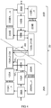
- FIG. 1A, 1B, 1C schematically shows an embodiment of the improved communication system 10.
- FIG. 1A shows an overview of the communication system
- FIG. 1B and 1C show a first module 100 being an optic transmitter and a second module 200 being an optic receiver, in more detail.
- the first module being the optic transmitter 100 comprises a plurality of lasers 110_1, 110_2,...,110_n , a wavelength division multiplexer 120, and a transmission unit 130.
- the plurality of lasers 110_1, 110_2, ..., 110_n provide respective optic output signals O1, O2, ..., On in respective wavelength channels. Modulation of the respective optic output signals may be achieved in various ways. According to a first approach (direct modulation) a laser is directly controlled. According to a second approach (external modulation), this is achieved by an external mechanism.
- the wavelength division multiplexer 120 multiplexes the optic output signals O1, O2, ..., On into a bundled optic output signal Oc, and the transmission unit 130 transmits the bundled optic output signal Oc as a transmitted optic output signal Otrans.
- the transmission unit 130 may comprise various additional functionalities, such as a pointing functionality to accurately direct the bundled optic output signal towards an optical receiver, and to correct therewith for vibrations. As another example a pre-correction functionality may be included to correct for anticipated effects of atmospheric perturbations.
- the second module 200 being the optic receiver comprises a receiving unit 210, a wavelength division demultiplexer 220 and a plurality of photon counters 230_1, 230_2,...,230_n.
- the receiving unit 210 receives the bundled optic input signal Orec that results from the bundled optic output signal Otrans after its propagation to the optic receiver and the wavelength division demultiplexer 220 demultiplexes this bundled optic input signal into respective optic signal components Oin_1, Oin_2,...,Oin_n in the respective wavelength channels.
- the photon counters 230_1, 230_2,...,230_n each provide respective photon count signals C1, C2,...,Cn for these optic signal components.
- the wavelength channels reserved for each optic output signals O1, O2, ..., On, to be detected as optic signal components Oin_1, Oin_2,...,Oin_n may have a bandwidth of a few pm to a few tens of nm depending on the technology used.
- the lasers 110_1, 110_2, ..., 110_n may for example have an output power in the range of a few mW or lower. In embodiments one, more or all of the lasers may be configured to provide their optic output signals in a pulse wise manner. In some embodiments the optic output signals may be provided as single photon pulses.
- An additional laser 115 may be included to provide a beacon signal BC.
- the beacon signal typically has a higher power then that of the optic output signals O1, O2, ..., On. It may be pulsed to keep power consumption low.
- the beacon signal is typically provided in parallel with the optic output signals O1, O2, ..., On in the bundled optic output signal Oc.
- the plurality of lasers 110_1, 110_2, ..., 110_n is integrated in a single photonic integrated circuit 112, as schematically indicated by a dotted box.
- the wavelength division multiplexer 120 may be integrated with the plurality of lasers 110_1, 110_2, ..., 110_n in a single photonic integrated circuit (indicated as dotted box 122).
- the optic transmitter 100 may be entirely provided as a single photonic integrated circuit.
- the elements of the transmitter may be provided as bulk components or may be optically coupled by optic fiber connections.
- the receiving unit 210 of the optic receiver 200 typically comprises pointing means, for example using an adaptive optic element, that is controlled on the basis of the beacon signal.
- the optic transmitter 100 typically has a pointing means to properly direct the bundled optic output signal Oc as a transmitted optic output signal Otrans towards the optic receiver 200, for example based on feedback signals from the optic receiver 200, or from a retroreflector being part of the receiver.
- the wavelength division demultiplexer 220 may use spectral filtering to demultiplex the bundled optic input signal into respective optic signal components Oin_1, Oin_2, ...,Oin_n.
- photon counters are a photomultiplier, Geiger counter, single-photon avalanche diode, high TRL photon avalanche diode, superconducting nanowire single-photon detector, transition edge sensor, or scintillation counter. Charge-coupled devices can also sometimes be used.
- the wavelength division demultiplexer 120 and the photon counters 230a, 230b, ...., 230n may be integrated in a single photonic integrated circuit.
- the optic receiver 200 may be entirely provided as a single photonic integrated circuit.
- the receiving unit 210 and the wavelength division multiplexer 220 may be integrated in single photonic integrated circuit, for example via photonic phased array interface using bulk optics for pointing the receiver towards the associated transmitter.
- FIG. 2 shows an embodiment of an optic communication arrangement 20 that comprises a first and a second optic transceiver 20A, 20B.
- the first optic transceiver 20A comprises a first optic transmitter 100A and a first optic receiver 200A.
- the second optic transceiver 20B comprises a second optic transmitter 100B and a second optic receiver 200B.
- the first optic transmitter 100A and the first optic receiver 200A are provided as a first photonic integrated circuit 22 at a first location and the second optic transmitter 100B and the second optic receiver 200B are provided as a second photonic integrated circuit 24 at a second location.
- FIG. 3 shows in more detail an embodiment of the optic communication arrangement 20 of FIG. 2 .
- the first optic transceiver 20A comprises in addition to the first optic transmitter 100A and the first optic receiver 200A also a first modem 300A.
- the second optic transceiver 20B comprises in addition to a second optic transmitter 100B and a second optic receiver 200B also a second modem 300B.
- the first optic transmitter 100A and the first optic receiver 200A share a common PAT-unit that has the functionality of a first transmission unit 130A and a receiving unit 210A.
- the common PAT-unit may provide common facilities for pointing and receiving.
- the PAT-unit has an active pointing functionality (such as moving mirrors or phased array) that directs the bundle in the desired direction.
- the incoming bundle comes from almost the same direction.
- the angle difference between the transmit and receive bundle is the point-ahead angle (PAA). This angle anticipates displacements of the terminals occurring during transmission of the signal between the transceivers 20A and 20B.
- the PAA is often small, so that the transmitted and received bundle can partly traverse a shared optical path.
- phased array for example based on PIC technology (such as photonic phased array) may be contemplated. This avoids use of expensive mirrors, so that from a cost perspective there is no need to have a shared optical path for receiving and transmitting functionalities. For example, but not necessarily a phased array per wavelength may be provided so that the beam is completely spatially multiplexed.
- units 120 and 220 may be integrated.
- the first modem 300A receives input signals, e.g. electric or optic input signals, from an external interface ExtA and issues a set of control signals CO1 A ,...,COn A .
- respective lasers 110A_1, ...,n provide respective optic output signals O1 A ,...,On A in respective wavelength channels with a respective wavelength range, each having a respective central wavelength ⁇ _1, ..., ⁇ _ n .
- the lasers 110A_1, ...,n and respective drivers are provided in a photonic integrated circuit.
- Such a product is for example available from Lionix using a hybrid assembly approach wherein low-loss silicon-nitride PIC is combined with active gain PICs.
- tunable gain section PIC in InP technology is hybridly attached to a tunable reflector PIC, therewith creating an external cavity laser.
- the gain section creates the first mirror and the necessary gain, whereas the silicon-nitride based TriPleXTM PIC acts as a tunable wavelength dependent mirror.
- wavelength channels with a very narrow bandwidth, e.g. a Lorentz linewidth of less than 10 kHz can be achieved.
- the wavelength channels may for example be provided within an overall range extending between 1530-1565 nm. But also other wavelength ranges are feasible.
- the wavelength division multiplexer 120A bundles these optic output signals into a bundled optic output signal Oc A and provides the bundled optic output signal Oc A to the PAT-unit 130A+210A.
- the wavelength division multiplexer 120A may also be provided in the same photonic integrated circuit as the lasers, but may alternatively be a separate unit, for example also a photonic integrated circuit or fiber based. Fiber optic couplers for this purpose are for example provided by Newport. An example thereof is a 1 x 16 fiber optic coupler of type F-CPL-F16150.
- the PAT-unit 130A+210A transmits the bundled optic output signal Oc A as a transmitted optic output signal OtransA through free space 400 to the second optic transceiver 20B.
- the PAT-unit 130A+210A is implemented as a photonic phased array in a photonic integrated circuit.
- Such an approach is described by McManamon et al. in "Optical phased array technology", Proceedings of the IEEE (Volume: 84 , Issue: 2 , Feb. 1996), page(s): 268 - 298 DOI: 10.1109/5.482231 .
- a phase profile is imposed on an optical beam as it is either transmitted through or reflected from the phase shifter array.
- the imposed phase profile steers, focuses, fans out, or corrects phase aberrations on the beam.
- the array of optical phase shifters is realized through lithographic patterning of an electrical addressing network on the superstrate of a liquid crystal waveplate. Refractive index changes sufficiently large to realize full-wave differential phase shifts can be effected using low ( ⁇ 10 V) voltages applied to the liquid crystal phase plate electrodes.
- the second optic transmitter 100B and the second optic receiver 200B likewise share a common PAT-unit that has the functionality of a second transmission unit 130B and a second receiving unit 210B.
- the common PAT-unit may provide common facilities for pointing and receiving.
- the common PAT-unit in its functionality as the second receiving unit 210B receives a bundled optic input signal Orec B resulting from the transmitted bundled optic output signal OtransA after its propagation through free space 400 to the second optic transceiver 20B.
- the wavelength division demultiplexer 220B of the second optic transceiver 20B demultiplexes the bundled optic input signal Orec B into respective optic signal components I1 B , I2 B , ...,In B .
- the wavelength division demultiplexer 220B may be implemented as a photonic integrated circuit, for example available from Lionix, but may alternatively be implemented as a fiber based unit.
- respective photon counters 230_1, 230_2, ...., 230_n provide respective photon count signals C1 B , C2 B , ..., Cn B for these optic signal components.
- the second modem 300B in response to these photon count signals C1 B , C2 B , ..., Cn B provides an output signal to the external interface ExtB.
- a photon counter for this purpose is a superconducting nanowire single photon detector (SNSPD) as provided by Single Quantum. This detector is constituted by a thin film of superconducting material shaped into a meandering nanowire.
- APD avalanche photodiode
- the optic communication arrangement 20 is provided in a symmetric manner. I.e. the first optic transceiver 20A and the second optic transceiver 20B are identical, or at least have the same functionality. According, in operation a signal provided at the external interface ExtB may be transmitted to the external interface as follows.
- the second modem 300B receives input signals, e.g. electric or optic input signals, from the external interface ExtB and issues a set of control signals CO1 B ,...,Con B .
- respective lasers 110B_1,...,n provide respective optic output signals O1 B ,...,On B in respective wavelength channels with a respective wavelength range.
- the wavelength division multiplexer 120B bundles these optic output signals into a bundled optic output signal Oc B and provides the bundled optic output signal Oc B to the PAT-unit 130B+210B which transmits the bundled optic output signal Oc B as a transmitted optic output signal Otrans B through free space 400 to the first optic transceiver 20A.
- these functionalities can be implemented by a common photonic phased array.
- the common PAT-unit in its functionality as the first receiving unit 210A receives a bundled optic input signal OrecA resulting from the transmitted bundled optic output signal Otrans B after its propagation through free space 400 to the first optic transceiver 20A.
- the wavelength division demultiplexer 220A of the first optic transceiver 20A demultiplexes the bundled optic input signal OrecA into respective optic signal components I1 A , I2 A , ...,In A .
- respective photon counters 230_1, 230_2, ...., 230_n provide respective photon count signals C1 A , C2 A , ..., Cn A for these optic signal components.
- the first modem 300A in response to these photon count signals C1 A , C2 A , ..., Cn A provides an output signal to the external interface ExtA.
- PAT-units 130A+210A and 130B+210B with pointing and receiving means.
- these are provided as bulk optics, e.g. using actuated mirrors.
- the pointing and receiving means may be implemented in a photonic integrated circuit, e.g. as a photonic phased array.
- FIG. 4 shows in more detail another embodiment of the optic communication arrangement 20 of FIG. 2 . Parts therein corresponding to those in FIG. 3 have the same reference number.
- the optic transceiver 20A comprises in addition to the elements presented in, and described with reference to FIG. 3 a beacon laser/amplifier unit 140A and optics multiplexing unit 150A.
- the beacon laser/amplifier unit 140A is a regular (space qualified) laser, optional provided with an optic amplifier to boost the power.
- a high power beacon can be used for very fast characterization of atmospheric disturbance.
- An optic beacon signal facilitates acquisition using adaptive optics (adaptive optics for correction of atmospheric disturbances in order to enable a coupling from free space to a fiber or PIC based optical component.
- a beacon is not needed if the optic signal is not transmitted in free space characterized by atmospheric disturbance but for example via a fiber or PIC coupling.
- the optic transceiver 20B comprises in addition to the elements presented in, and described with reference to FIG. 3 a beacon laser/amplifier unit 140B and optics multiplexing unit 150B.
- the beacon laser/amplifier unit 140A is controlled to issue a high power beacon signal OB A
- the optics multiplexing unit 150A bundles this optic signal with the bundled optic signal OCA into the bundled optic signal OD A . It may be contemplated to provide the beacon signal OB A as a further optic input signal to the wavelength division multiplexer 120A.
- the separate optics multiplexing unit 150A that multiplexes the high power beacon signal OB A , with the bundled optic signal OCA into the bundled optic signal OD A can for example be implemented with fiber optic means.
- This bundled optic signal OD A is provided to the pointing acquisition and tracking unit (PAT-unit) 130A+210A which transmits the bundled optic output signal OD A as a transmitted optic output signal to the second optic transceiver 20B.
- the high power beacon signal OB A may be time-multiplexed with the bundled optic signal OCA into the bundled optic signal OD A , so that the PAT-unit 130B+210B can periodically align itself during relatively short time intervals using the relatively high power beacon signal OB A , and information transmission can take place during the remaining time intervals via the bundled optic signal Oc A
- the optionally pulsed beacon signal OB A may be transmitted while information transmission takes place.
- the beacon laser/amplifier unit 140B is controlled to issue a high power beacon signal OB B , and the optics multiplexing unit 150B bundles this optic signal with the bundled optic signal OC B into the bundled optic signal OD B .
- This bundled optic signal OD B is provided to the PAT-unit 130B+210B which transmits the bundled optic output signal OD B as a transmitted optic output signal to the first optic transceiver 20A.
- FIG. 5A schematically shows an embodiment of an optic communication method as claimed herein comprising method steps S1 - S6.
- step S1 respective optic output signals are provided in respective wavelength channels having a respective wavelength range.
- step S2 the optic output signals provided in step S1 are bundled into a bundled optic output signal.
- step S3 the bundled optic output signal is transmitted.
- step S4 a bundled optic input signal resulting from the bundled optic output signal after its propagation is received.
- step S5 the bundled optic input signal is demultiplexed into respective optic signal components in the respective wavelength channels.
- step S6 respective photon count signals are provided for the respective optic signal components.
- FIG. 5B shows another embodiment of the claimed optic communication method.
- method steps S10, S20, S30, S40, S50 and S60 correspond to steps S1, S2, S3, S4, S5 and S6 respectively.
- An optic beacon signal with a relatively high power is generated in step S11.
- step S21 the optic beacon signal is aligned, so that it has at least substantially the same beam characteristics, i.e.
- step S30 the beacon signal is transmitted in the same manner as the bundled optic output signal would be transmitted in step S3 of FIG. 5A or in step S30 in FIG. 5B when operating in the first operational mode M1.
- step S40 an input beacon signal resulting from the beacon signal after its propagation is received in the same manner as the bundled optic input signal would be received in step S4 of FIG. 5A or in step S40 in FIG. 5B when operating in the first operational mode M1.
- step S51 the input beacon signal is guided to a detector facility to be detected in step S61 and in step S65 the detection signals are used for mutual alignment of the transmitting and receiving side.
Landscapes
- Physics & Mathematics (AREA)
- Electromagnetism (AREA)
- Engineering & Computer Science (AREA)
- Computer Networks & Wireless Communication (AREA)
- Signal Processing (AREA)
- Optical Communication System (AREA)
Priority Applications (2)
| Application Number | Priority Date | Filing Date | Title |
|---|---|---|---|
| EP20154568.8A EP3859999A1 (de) | 2020-01-30 | 2020-01-30 | Optisches kommunikationsverfahren, system, sender und empfänger |
| PCT/NL2021/050060 WO2021154082A1 (en) | 2020-01-30 | 2021-02-01 | Optic communication method, system, transmitter and receiver |
Applications Claiming Priority (1)
| Application Number | Priority Date | Filing Date | Title |
|---|---|---|---|
| EP20154568.8A EP3859999A1 (de) | 2020-01-30 | 2020-01-30 | Optisches kommunikationsverfahren, system, sender und empfänger |
Publications (1)
| Publication Number | Publication Date |
|---|---|
| EP3859999A1 true EP3859999A1 (de) | 2021-08-04 |
Family
ID=69411305
Family Applications (1)
| Application Number | Title | Priority Date | Filing Date |
|---|---|---|---|
| EP20154568.8A Withdrawn EP3859999A1 (de) | 2020-01-30 | 2020-01-30 | Optisches kommunikationsverfahren, system, sender und empfänger |
Country Status (2)
| Country | Link |
|---|---|
| EP (1) | EP3859999A1 (de) |
| WO (1) | WO2021154082A1 (de) |
Families Citing this family (4)
| Publication number | Priority date | Publication date | Assignee | Title |
|---|---|---|---|---|
| CN113595632B (zh) * | 2021-08-10 | 2023-12-12 | 长春理工大学 | 一种基于多单元拼接阵列的空间激光通信方法和系统 |
| US11770189B2 (en) | 2021-09-17 | 2023-09-26 | Honeywell Limited Honeywell Limitée | Optical communication system using a photonic lantern |
| US12362828B2 (en) | 2022-04-08 | 2025-07-15 | Honeywell Limited Honeywell Limitée | Optical communication system using a photonic lantern for fine point tracking |
| CN116506015B (zh) * | 2023-02-17 | 2026-04-17 | 香港中文大学(深圳) | 波分复用系统、设备、波分复用通信方法及介质 |
Citations (3)
| Publication number | Priority date | Publication date | Assignee | Title |
|---|---|---|---|---|
| WO2018125290A1 (en) * | 2016-12-29 | 2018-07-05 | Booz Allen Hamilton Inc. | M-ary frequency presence modulation communication system and method |
| WO2018227005A1 (en) * | 2017-06-07 | 2018-12-13 | Ii-Vi Delaware, Inc. | Integrated wdm optical transceiver |
| US20190115979A1 (en) | 2016-02-01 | 2019-04-18 | California Institute Of Technology | Optical communication systems |
Family Cites Families (2)
| Publication number | Priority date | Publication date | Assignee | Title |
|---|---|---|---|---|
| US8073342B2 (en) * | 2007-05-04 | 2011-12-06 | Massachusetts Institute Of Technology | Method and apparatus for transmitting optical signals |
| GB2534917B (en) * | 2015-02-05 | 2017-09-27 | Toshiba Res Europe Ltd | A quantum communication system and a quantum communication method |
-
2020
- 2020-01-30 EP EP20154568.8A patent/EP3859999A1/de not_active Withdrawn
-
2021
- 2021-02-01 WO PCT/NL2021/050060 patent/WO2021154082A1/en not_active Ceased
Patent Citations (3)
| Publication number | Priority date | Publication date | Assignee | Title |
|---|---|---|---|---|
| US20190115979A1 (en) | 2016-02-01 | 2019-04-18 | California Institute Of Technology | Optical communication systems |
| WO2018125290A1 (en) * | 2016-12-29 | 2018-07-05 | Booz Allen Hamilton Inc. | M-ary frequency presence modulation communication system and method |
| WO2018227005A1 (en) * | 2017-06-07 | 2018-12-13 | Ii-Vi Delaware, Inc. | Integrated wdm optical transceiver |
Non-Patent Citations (1)
| Title |
|---|
| YUZO YOSHIKUNI: "Recent Progress of Semiconductor Integrated Optics for WDM Photonic Networks", 2003 PROCEEDINGS- EUROPEAN CONFERENCE ON INTEGRATED OPTICS, 1 January 2003 (2003-01-01), pages 1 - 10, XP055555603, Retrieved from the Internet <URL:https://www.ecio-conference.org/wp-content/uploads/2016/05/2003/2003_ThP3.pdf> [retrieved on 20190212] * |
Also Published As
| Publication number | Publication date |
|---|---|
| WO2021154082A1 (en) | 2021-08-05 |
Similar Documents
| Publication | Publication Date | Title |
|---|---|---|
| CN113227864B (zh) | 面板式可插拔远程激光源和包含所述激光源的系统 | |
| EP3859999A1 (de) | Optisches kommunikationsverfahren, system, sender und empfänger | |
| US8965203B1 (en) | Flexible non-modular data center with reconfigurable extended-reach optical network fabric | |
| US7450858B2 (en) | Apparatus and method for transmitting and receiving wavelength division multiplexing signals | |
| Buscaino et al. | External vs. integrated light sources for intra-data center co-packaged optical interfaces | |
| US10439727B2 (en) | Method and system for selectable parallel optical fiber and wavelength division multiplexed operation | |
| US9225454B1 (en) | Aggregation and de-agreggation of bandwidth within data centers using passive optical elements | |
| US8355612B2 (en) | Active alignment method for multi-channel optical transmitter and receiver, which has an optical signal generator with an optical multiplexer, which has an optical signal generator with an optical multiplexer | |
| US20190165200A1 (en) | Method And System For A Focused Field Avalanche Photodiode | |
| US7386235B2 (en) | Protocol and line-rate transparent WDM passive optical network | |
| CN110892655A (zh) | 集成wdm光收发器 | |
| US7539418B1 (en) | Integrated ring modulator array WDM transceiver | |
| US20170201341A1 (en) | Optical spatial division multiplexing usable at short reach | |
| CN117178197A (zh) | 一种光功率分配系统 | |
| EP1356620B1 (de) | Optisches wdm-kommunikationssystem | |
| Liu | Integrated silicon photonics links for high bandwidth data transportation | |
| US7019907B2 (en) | Integrated lithium niobate based optical transmitter | |
| US11057113B1 (en) | High-speed silicon photonics optical transceivers | |
| US9185475B1 (en) | Signal quality in bi-directional optical links using optical circulators | |
| US10020888B1 (en) | Transmitter and receiver for direct communication of multiple optical wavelengths via an optical link | |
| KR20240157070A (ko) | 베이스밴드 유닛 및 액세스 네트워크 디바이스 | |
| Akulova et al. | Scalable heterogeneously integrated silicon photonics technology platform and its applications | |
| US7444079B2 (en) | Optical power control monitor for multiple wavelength fiber-optic networks | |
| Bassinan et al. | Toward future generation digital avionics fiber optic communication | |
| EP1612974B1 (de) | Protokoll- und Leitungsgeschwindingkeits-transparentes WDM passives optisches Netzwerk |
Legal Events
| Date | Code | Title | Description |
|---|---|---|---|
| PUAI | Public reference made under article 153(3) epc to a published international application that has entered the european phase |
Free format text: ORIGINAL CODE: 0009012 |
|
| STAA | Information on the status of an ep patent application or granted ep patent |
Free format text: STATUS: THE APPLICATION HAS BEEN PUBLISHED |
|
| AK | Designated contracting states |
Kind code of ref document: A1 Designated state(s): AL AT BE BG CH CY CZ DE DK EE ES FI FR GB GR HR HU IE IS IT LI LT LU LV MC MK MT NL NO PL PT RO RS SE SI SK SM TR |
|
| STAA | Information on the status of an ep patent application or granted ep patent |
Free format text: STATUS: THE APPLICATION IS DEEMED TO BE WITHDRAWN |
|
| 18D | Application deemed to be withdrawn |
Effective date: 20220205 |