EP3860115A1 - Élément d'imagerie à semi-conducteurs, procédé de commande d'élément d'imagerie à semi-conducteurs et appareil électronique - Google Patents
Élément d'imagerie à semi-conducteurs, procédé de commande d'élément d'imagerie à semi-conducteurs et appareil électronique Download PDFInfo
- Publication number
- EP3860115A1 EP3860115A1 EP19864558.2A EP19864558A EP3860115A1 EP 3860115 A1 EP3860115 A1 EP 3860115A1 EP 19864558 A EP19864558 A EP 19864558A EP 3860115 A1 EP3860115 A1 EP 3860115A1
- Authority
- EP
- European Patent Office
- Prior art keywords
- light receiving
- unit
- photocurrent
- pixel
- receiving element
- Prior art date
- Legal status (The legal status is an assumption and is not a legal conclusion. Google has not performed a legal analysis and makes no representation as to the accuracy of the status listed.)
- Granted
Links
Images








Classifications
-
- H—ELECTRICITY
- H04—ELECTRIC COMMUNICATION TECHNIQUE
- H04N—PICTORIAL COMMUNICATION, e.g. TELEVISION
- H04N25/00—Circuitry of solid-state image sensors [SSIS]; Control thereof
- H04N25/60—Noise processing, e.g. detecting, correcting, reducing or removing noise
- H04N25/63—Noise processing, e.g. detecting, correcting, reducing or removing noise applied to dark current
-
- H—ELECTRICITY
- H04—ELECTRIC COMMUNICATION TECHNIQUE
- H04N—PICTORIAL COMMUNICATION, e.g. TELEVISION
- H04N25/00—Circuitry of solid-state image sensors [SSIS]; Control thereof
- H04N25/40—Extracting pixel data from image sensors by controlling scanning circuits, e.g. by modifying the number of pixels sampled or to be sampled
-
- H—ELECTRICITY
- H04—ELECTRIC COMMUNICATION TECHNIQUE
- H04N—PICTORIAL COMMUNICATION, e.g. TELEVISION
- H04N25/00—Circuitry of solid-state image sensors [SSIS]; Control thereof
- H04N25/47—Image sensors with pixel address output; Event-driven image sensors; Selection of pixels to be read out based on image data
-
- H—ELECTRICITY
- H04—ELECTRIC COMMUNICATION TECHNIQUE
- H04N—PICTORIAL COMMUNICATION, e.g. TELEVISION
- H04N25/00—Circuitry of solid-state image sensors [SSIS]; Control thereof
- H04N25/70—SSIS architectures; Circuits associated therewith
- H04N25/703—SSIS architectures incorporating pixels for producing signals other than image signals
- H04N25/707—Pixels for event detection
-
- H—ELECTRICITY
- H04—ELECTRIC COMMUNICATION TECHNIQUE
- H04N—PICTORIAL COMMUNICATION, e.g. TELEVISION
- H04N25/00—Circuitry of solid-state image sensors [SSIS]; Control thereof
- H04N25/70—SSIS architectures; Circuits associated therewith
- H04N25/76—Addressed sensors, e.g. MOS or CMOS sensors
- H04N25/77—Pixel circuitry, e.g. memories, A/D converters, pixel amplifiers, shared circuits or shared components
- H04N25/771—Pixel circuitry, e.g. memories, A/D converters, pixel amplifiers, shared circuits or shared components comprising storage means other than floating diffusion
-
- H—ELECTRICITY
- H04—ELECTRIC COMMUNICATION TECHNIQUE
- H04N—PICTORIAL COMMUNICATION, e.g. TELEVISION
- H04N25/00—Circuitry of solid-state image sensors [SSIS]; Control thereof
- H04N25/70—SSIS architectures; Circuits associated therewith
- H04N25/76—Addressed sensors, e.g. MOS or CMOS sensors
- H04N25/77—Pixel circuitry, e.g. memories, A/D converters, pixel amplifiers, shared circuits or shared components
- H04N25/772—Pixel circuitry, e.g. memories, A/D converters, pixel amplifiers, shared circuits or shared components comprising A/D, V/T, V/F, I/T or I/F converters
-
- H—ELECTRICITY
- H04—ELECTRIC COMMUNICATION TECHNIQUE
- H04N—PICTORIAL COMMUNICATION, e.g. TELEVISION
- H04N25/00—Circuitry of solid-state image sensors [SSIS]; Control thereof
- H04N25/70—SSIS architectures; Circuits associated therewith
- H04N25/76—Addressed sensors, e.g. MOS or CMOS sensors
- H04N25/78—Readout circuits for addressed sensors, e.g. output amplifiers or A/D converters
-
- H—ELECTRICITY
- H10—SEMICONDUCTOR DEVICES; ELECTRIC SOLID-STATE DEVICES NOT OTHERWISE PROVIDED FOR
- H10F—INORGANIC SEMICONDUCTOR DEVICES SENSITIVE TO INFRARED RADIATION, LIGHT, ELECTROMAGNETIC RADIATION OF SHORTER WAVELENGTH OR CORPUSCULAR RADIATION
- H10F30/00—Individual radiation-sensitive semiconductor devices in which radiation controls the flow of current through the devices, e.g. photodetectors
- H10F30/20—Individual radiation-sensitive semiconductor devices in which radiation controls the flow of current through the devices, e.g. photodetectors the devices having potential barriers, e.g. phototransistors
-
- H—ELECTRICITY
- H10—SEMICONDUCTOR DEVICES; ELECTRIC SOLID-STATE DEVICES NOT OTHERWISE PROVIDED FOR
- H10F—INORGANIC SEMICONDUCTOR DEVICES SENSITIVE TO INFRARED RADIATION, LIGHT, ELECTROMAGNETIC RADIATION OF SHORTER WAVELENGTH OR CORPUSCULAR RADIATION
- H10F39/00—Integrated devices, or assemblies of multiple devices, comprising at least one element covered by group H10F30/00, e.g. radiation detectors comprising photodiode arrays
- H10F39/10—Integrated devices
- H10F39/12—Image sensors
-
- H—ELECTRICITY
- H10—SEMICONDUCTOR DEVICES; ELECTRIC SOLID-STATE DEVICES NOT OTHERWISE PROVIDED FOR
- H10F—INORGANIC SEMICONDUCTOR DEVICES SENSITIVE TO INFRARED RADIATION, LIGHT, ELECTROMAGNETIC RADIATION OF SHORTER WAVELENGTH OR CORPUSCULAR RADIATION
- H10F39/00—Integrated devices, or assemblies of multiple devices, comprising at least one element covered by group H10F30/00, e.g. radiation detectors comprising photodiode arrays
- H10F39/80—Constructional details of image sensors
- H10F39/802—Geometry or disposition of elements in pixels, e.g. address-lines or gate electrodes
- H10F39/8023—Disposition of the elements in pixels, e.g. smaller elements in the centre of the imager compared to larger elements at the periphery
-
- H—ELECTRICITY
- H10—SEMICONDUCTOR DEVICES; ELECTRIC SOLID-STATE DEVICES NOT OTHERWISE PROVIDED FOR
- H10F—INORGANIC SEMICONDUCTOR DEVICES SENSITIVE TO INFRARED RADIATION, LIGHT, ELECTROMAGNETIC RADIATION OF SHORTER WAVELENGTH OR CORPUSCULAR RADIATION
- H10F39/00—Integrated devices, or assemblies of multiple devices, comprising at least one element covered by group H10F30/00, e.g. radiation detectors comprising photodiode arrays
- H10F39/80—Constructional details of image sensors
- H10F39/803—Pixels having integrated switching, control, storage or amplification elements
- H10F39/8037—Pixels having integrated switching, control, storage or amplification elements the integrated elements comprising a transistor
-
- H—ELECTRICITY
- H10—SEMICONDUCTOR DEVICES; ELECTRIC SOLID-STATE DEVICES NOT OTHERWISE PROVIDED FOR
- H10F—INORGANIC SEMICONDUCTOR DEVICES SENSITIVE TO INFRARED RADIATION, LIGHT, ELECTROMAGNETIC RADIATION OF SHORTER WAVELENGTH OR CORPUSCULAR RADIATION
- H10F39/00—Integrated devices, or assemblies of multiple devices, comprising at least one element covered by group H10F30/00, e.g. radiation detectors comprising photodiode arrays
- H10F39/80—Constructional details of image sensors
- H10F39/805—Coatings
- H10F39/8057—Optical shielding
-
- H—ELECTRICITY
- H10—SEMICONDUCTOR DEVICES; ELECTRIC SOLID-STATE DEVICES NOT OTHERWISE PROVIDED FOR
- H10F—INORGANIC SEMICONDUCTOR DEVICES SENSITIVE TO INFRARED RADIATION, LIGHT, ELECTROMAGNETIC RADIATION OF SHORTER WAVELENGTH OR CORPUSCULAR RADIATION
- H10F39/00—Integrated devices, or assemblies of multiple devices, comprising at least one element covered by group H10F30/00, e.g. radiation detectors comprising photodiode arrays
- H10F39/80—Constructional details of image sensors
- H10F39/813—Electronic components shared by multiple pixels, e.g. one amplifier shared by two pixels
Definitions
- the present invention relates to a solid-state imaging device, a method of controlling a solid-state imaging device, and an electronic device.
- CMOS complementary metal oxide semiconductor
- a detection circuit that detects, as an address event, a signal indicating that the amount of light received by a light receiving element in each pixel exceeds a threshold value in real time is provided for each pixel
- DVS dynamic vision sensor
- Patent Literature 1 Japanese Laid-open Patent Publication No. 2017-535999
- the asynchronous solid-state imaging device such as this DVS is used, and thus, a faster response can be performed compared to a case where the existing synchronous solid-state imaging device that captures image data synchronized with a synchronization signal such as a vertical synchronizing signal is used.
- a synchronization signal such as a vertical synchronizing signal
- An object of the present disclosure is to enable utilization of a solid-state imaging device that detects an address event by more various methods.
- a solid-state imaging device has a plurality of pixels arrayed in a two-dimensional lattice; and a control unit, wherein the pixel includes a first light receiving element that outputs a first photocurrent corresponding to received light, a second light receiving element that outputs a second photocurrent corresponding to received light, a conversion unit that converts a current into a voltage, an output unit that detects an event based on a change in the voltage converted by the conversion unit, and outputs a detection signal indicating a detection result of the detection, and a switch unit that performs switching of switching the current to be converted into the voltage by the conversion unit between the first photocurrent and the second photocurrent, and the control unit controls the switching performed by the switch unit.
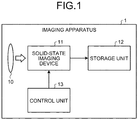
- the solid-state imaging device 11 includes pixels each including a plurality of light receiving elements that converts incident light rays into electric signals by photoelectric conversion and outputs the electric signals, and a drive circuit that drives the pixels.
- the solid-state imaging device 11 further includes a signal processing unit that performs predetermined signal processing on the signal output from the pixel and outputs the signal as output data.
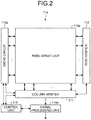
- FIG. 2 is a block diagram illustrating a configuration of an example of a solid-state imaging device 11a applicable to the first embodiment which corresponds to the above-mentioned solid-state imaging device 11.
- the solid-state imaging device 11a includes a pixel array unit 110a, a column arbiter 111, a row arbiter 112, a drive circuit 113a, a signal processing unit 114a, and a control unit 115.
- a plurality of pixels is arrayed in a two-dimensional lattice.
- an array in a horizontal direction in FIG. 2 is referred to as a "row”
- an array in a direction perpendicular to the row is referred to as a "column”.
- Each pixel included in the pixel array unit 110a includes a plurality of light receiving elements that outputs photocurrents corresponding to the received light rays, and an address event detection unit that detects an address event based on the amount of changes in the photocurrents output from the plurality of light receiving elements.
- Each pixel outputs a request to the column arbiter 111 and the row arbiter 112 according to the occurrence of the address event.
- the column arbiter 111 and the row arbiter 112 perform arbitration in cooperation with each other according to the request output from each pixel included in the pixel array unit 110a, and select an event detection signal output from a specific pixel.
- the selected event detection signal is output from the column arbiter 111.
- the column arbiter 111 and the row arbiter 112 output address information for specifying the pixel that outputs the selected event detection signal together with the event detection signal.
- the drive circuit 113a drives each of the pixels to cause each pixel to execute the address event detection.
- the drive circuit 113a drives the pixels included in the pixel array unit 110a in units of rows.
- the pixels included in the pixel array unit 110a are driven in a column direction and a row direction, and thus, an address event detection operation can be executed for each pixel.
- the event detection signal and the address information output from the column arbiter 111 are supplied to the signal processing unit 114a.
- the signal processing unit 114a executes signal processing such as image recognition processing based on the event detection signal and the address information.
- the signal processing unit 114a outputs, as output data, event detection data indicating the processing result, and supplies the output data to the storage unit 120.
- the solid-state imaging device 11a described with reference to FIG. 2 can be formed as, for example, a stacked contact image sensor (CIS) formed by stacking a plurality of semiconductor chips.
- the solid-state imaging device 11a can be formed by a two-layer structure in which semiconductor chips are stacked in two layers.
- FIG. 3 is a diagram illustrating an example in which the solid-state imaging device 11a according to the first embodiment is formed by the stacked CIS having the two-layer structure.
- a light receiving chip 201 including, for example, the light receiving element is formed on the first-layer semiconductor chip
- a detection chip 202 including the address event detection unit that detects the address event based on the photocurrent output from the light receiving element is formed on the second-layer semiconductor chip.
- the solid-state imaging device 11a is formed as one sensor by bonding the first-layer semiconductor chip and the second-layer semiconductor chip while electrically bringing into contact with each other.
- FIG. 4 is a block diagram illustrating a configuration of an example of the pixel array unit 110a applicable to the first embodiment.
- the pixel array unit 110a includes a plurality of pixels 20a arrayed in a two-dimensional lattice.
- each pixel 20a includes an address event detection unit 30 and a light receiving unit 40a.
- the light receiving unit 40a includes a plurality of light receiving elements. Each of the plurality of light receiving elements photoelectrically converts the incident light, and generates the photocurrent. The light receiving unit 40a supplies the photocurrent generated by the light receiving element selected from among the plurality of light receiving elements to the address event detection unit 30 under the control of the drive circuit 113a.
- the address event detection unit 30 determines whether or not the amount of change in the photocurrent supplied from the light receiving unit 40a exceeds a threshold value, and detects the presence or absence of the address event based on the determination result.
- the address event includes, for example, an up event indicating that the amount of change in the photocurrent exceeds an ON threshold value, and a down event indicating that the amount of change is less than an OFF threshold value.
- the event detection signal indicating the detection of the address event includes, for example, 1 bit indicating the detection result of the up event and 1 bit indicating the detection result of the down event.
- the address event detection unit 30 can also detect only the up event.
- the address event detection unit 30 When the occurrence of the address event is detected, the address event detection unit 30 requests the column arbiter 111 and the row arbiter 112 to transmit the event detection signal indicating the occurrence of the address event. When a response to this request is received from the column arbiter 111 and the row arbiter 112, the address event detection unit 30 supplies an address detection signal to the signal processing unit 114a via the column arbiter 111.
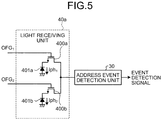
- FIG. 5 is a diagram illustrating a configuration of an example of the light receiving unit 40a according to the first embodiment.
- the light receiving unit 40a includes two light receiving elements 401a and 401b which are, for example, photodiodes (PD).
- PD photodiodes
- a cathode is connected to the ground, and an anode is connected to a source of a transistor 400a which is an N-type MOS transistor.
- a drain of the transistor 400a is connected to the address event detection unit 30.
- a signal OFG 1 is supplied to a gate of the transistor 400a.
- the transistor 400a is turned on when the signal OFG 1 is in a high state, and is turned off when the signal OFG 1 is in a low state.
- a photocurrent Iph 1 output from the light receiving element 401a is supplied to the address event detection unit 30.
- a cathode is connected to the ground, and an anode is connected to a source of a transistor 400b which is an N-type MOS transistor.
- a drain of the transistor 400b is connected to the address event detection unit 30 in common with the drain of the above-mentioned transistor 400a.
- a signal OFG 2 is supplied to a gate of the transistor 400b.
- the transistor 400b is turned on when the signal OFG 2 is in a high state, and is turned off when the signal OFG 2 is in a low state.
- a photocurrent Iph 2 output from the light receiving element 401b is supplied to the address event detection unit 30.
- the light receiving element 401a has sensitivity lower than the light receiving element 401b. That is, when light rays having the same amount of light are incident on the light receiving element 401a and the light receiving element 401b, a current value of the photocurrent Iph 1 output from the light receiving element 401a is smaller than a current value of the photocurrent Iph 2 output from the light receiving element 401b (Iph 1 ⁇ Iph 2 ).
- FIGS. 6A and 6B are diagrams illustrating examples of the pixel 20a including the light receiving elements 401a and 401b having different sensitivities.
- the light receiving elements 401a and 401b are also described as PD 1 and PD 2 , respectively.
- FIG. 6A is an example in which a sensitivity difference is generated by setting light receiving units of the light receiving elements 401a and 401b to have different areas.
- the area of the light receiving unit of the light receiving element 401a is smaller than the area of the light receiving unit of the light receiving element 401b.
- photoelectric conversion in the light receiving element 401a is performed less than in the light receiving element 401a. Accordingly, the light sensitivity of the light receiving element 401a is lower than that of the light receiving element 401b.
- FIG. 6B illustrates an example in which the light receiving elements 401a and 401b have the same configuration, and the areas of the light receiving units are the same, whereas a part of the light receiving unit of the light receiving element 401a (half in the example of FIG. 6B ) is shielded by a mask or the like.
- the light applied to the light receiving element 401a is incident on the light receiving unit in an opening region A, and is not incident on the light receiving unit in a light shielding region B.
- the light sensitivity of the light receiving element 401a is lower than that of the light receiving element 401b by setting the light receiving units of the light receiving elements 401a and 401b to have substantially different areas as in the example of FIG. 6A .
- FIG. 7 is a schematic diagram illustrating an example of wirings in the pixel array unit 110a according to the first embodiment.
- the drive circuit 113a generates the signals OFG 1 and OFG 2 under the control of the control unit 115, and supplies the generated signals OFG 1 and OFG 2 to each pixel 20a.
- the drive circuit 113a generates the signals OFG 1 and OFG 2 for each row for each of the pixels 20a arrayed in the two-dimensional lattice in the pixel array unit 110a.
- the pixels 20a are connected to the row arbiter 112 in units of rows in order to transmit and receive the requests and the responses. At this time, the pixels 20a are connected to the column arbiter 111 in units of columns in order to transmit and receive the requests and the responses and supply the event detection signal indicating the detection of the event and the address information.
- the column arbiter 111 supplies the event detection signal and the address information supplied from the pixel 20a to the control unit 115.
- the control unit 115 specifies the row in which the high and low states of the signals OFG 1 and OFG 2 need to be switched based on the event detection signal and the address information supplied from the column arbiter 111.
- the control unit 115 supplies an instruction to switch between the high and low states of the signals OFG 1 and OFG 2 in the specified row to the drive circuit 113a.
- the drive circuit 113a switches between the high and low states of the signals OFG 1 and OFG 2 in the row according to this instruction.
- the signals OFG 1 and OFG 2 are supplied in units of rows of the pixels 20a included in the pixel array unit 110a in the example of FIG. 7 , the present invention is not limited thereto.
- the signals OFG 1 and OFG 2 may be collectively supplied to all the pixels 20a included in the pixel array unit 110a, or the pixel array unit 110a may be divided into a plurality of blocks including a predetermined number of pixels 20a and the signals OFG 1 and OFG 2 may be supplied in units of blocks.
- FIG. 8 is a diagram illustrating a configuration of the address event detection unit 30 applicable to the first embodiment in more detail.
- the address event detection unit 30 includes a current-to-voltage conversion unit 300, a buffer amplifier 310, a subtraction unit 320, and a quantizer 330.
- the current-to-voltage conversion unit 300 includes transistors 301 and 303 which are N-type MOS transistors and a transistor 302 which is a P-type MOS transistor.
- the light receiving element 401a is a photodiode.
- FIG. 8 only the light receiving element 401a of the light receiving elements 401a and 401b included in the light receiving unit 40a is illustrated and the transistor 400a is not illustrated for the sake of convenience in description.
- a source of the N-type transistor 301 is connected to the light receiving element 401a, and a drain is connected to a power supply terminal.
- the P-type transistor 302 and the N-type transistor 303 are connected in series between the power supply terminal and a ground terminal.
- a connection point between a drain of the transistor 302 and a drain of the transistor 303 is connected to a gate of the transistor 301 and an input terminal of the buffer amplifier 310.
- a predetermined bias voltage V bs is applied to a gate of the transistor 302.
- the drains of the N-type transistors 301 and 303 are connected to a power supply side, and each form a source follower.
- the photocurrent output from the light receiving element 401a is converted into a logarithmic voltage signal by these two source followers connected in a loop.
- the transistor 302 supplies a constant current to the transistor 303.
- the voltage signal obtained by converting the photocurrent output from the light receiving element 401a into the voltage by the current-to-voltage conversion unit 300 is supplied to the subtraction unit 320 via the buffer amplifier.
- the subtraction unit 320 includes capacitors 321 and 322 having capacitances C 1 and C 2 , a switch unit 323, and an inverter 324.
- One terminal of the capacitor 321 is connected to an output terminal of the buffer amplifier, and the other terminal is connected to an input terminal of the inverter 324.
- the capacitor 322 is connected in parallel with the inverter 324.
- the switch unit 323 switches a path connecting both terminals of the capacitor 322 between an ON state and an OFF state according to a row drive signal.
- the inverter 324 inverts the voltage signal input via the capacitor 321.
- the inverter 324 supplies the inverted signal to the quantizer 330.
- a voltage signal V init which is an output signal of the buffer amplifier is input to a side of the capacitor 321 close to the buffer amplifier, and a side of the capacitor 321 close to the inverter 324 serves as a virtual ground terminal.
- a potential of this virtual ground terminal is set to zero for the sake of convenience in description.
- a charge Q init accumulated in the capacitor 321 is expressed by the following Equation (1) based on the capacitance C 1 of the capacitor 321. Meanwhile, since both terminals of the capacitor 322 are short-circuited by the switch unit 323, the accumulated charge becomes zero.
- Q init C 1 ⁇ V init
- Equation (5) represents a subtraction operation of the voltage signal, and a gain of the subtraction result is a ratio C 1 /C 2 of the capacitances of the capacitors 321 and 322.
- the capacitors are designed such that the capacitance C 1 of the capacitor 321 is large and the capacitance C 2 of the capacitor 322 is small.
- the capacitance C 2 of the capacitor 322 is too small, kTC noise may increase, and thus, there is a concern that noise characteristics deteriorate.
- the reduction of the capacitance C 2 of the capacitor 322 is limited to a range in which noise can be allowed.
- the capacitances C 1 and C 2 of the capacitors 321 and 322 have restrictions on the areas.
- the values of the capacitances C 1 and C 2 of the capacitors 321 and 322 are determined in consideration of these restrictions.
- the OFF threshold value and the ON threshold value are threshold values for the voltage V diff for detecting the down event and the up event, respectively.
- the voltage V diff exceeds the OFF threshold value in a positive direction, the up event is detected, and when the voltage V diff exceeds the ON threshold value in a negative direction, the down event is detected.
- the voltage V diff is less than the OFF threshold value and exceeds the ON threshold value, the event is not detected.
- the output voltage Vp output from the current-to-voltage conversion unit 300 is input to the subtraction unit 320 via the buffer amplifier.
- the amount of light received by the light receiving element 401a increases and the output voltage Vp output from the current-to-voltage conversion unit 300 increases will be described.
- the output voltage Vp increases from this point in time t 0 and the voltage V diff which is a difference of the output voltage Vp from the output voltage Vp at the point in time t 0 exceeds the ON threshold value in the negative direction at a point in time t 1 .
- the event detection signal indicating the up event detection is output from the quantizer 330.
- the switch unit 323 is switched to the ON state by the row drive circuit 110 according to this event detection signal, and the output of the subtraction unit 320 is set to the reset level.
- the row drive circuit 110 switches the switch unit 323 to the OFF state immediately after the output of the subtraction unit 320 is set to the reset level.
- the output voltage Vp is changed from an increase to a decrease at a point in time t 2 , and at a point in time t 3 , a difference between the output voltage Vp at the point in time t 3 and the output voltage Vp when it is determined to exceed the threshold value (in this case, the ON threshold value) immediately before the point in time t 3 exceeds the OFF threshold value in the positive direction. Accordingly, the event detection signal indicating the down event detection is output from the quantizer 330.
- the switch unit 323 is switched to the ON state by the row drive circuit 110 according to this event detection signal, and the output of the subtraction unit 320 is set to the reset level.
- the row drive circuit 110 switches the switch unit 323 to the OFF state immediately after the output of the subtraction unit 320 is set to the reset level.
- the address event detection unit 30 can output the event detection signal corresponding to a change in the amount of light received by the light receiving element 401a by comparing the difference of the output voltage Vp of the current-to-voltage conversion unit 300 with the ON threshold value and the OFF threshold value as described above.
- a voltage Vp' is obtained by rewriting the change in the output voltage Vp of the current-to-voltage conversion unit 300 on the upper side of FIG. 9 according to the lower side of FIG. 9 , that is, the output of the quantizer 330.
- the quantizer 330 detects rising and falling of the change in the voltage Vp' for each of the ON threshold value and the OFF threshold value from the determination result using the ON threshold value and the OFF threshold value based on a change in the voltage Vp' and the voltage V diff .
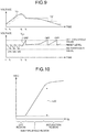
- FIG. 10 is a diagram illustrating an example of Vg-Id characteristics of the transistor 301 which the N-type MOS transistor used in the current-to-voltage conversion unit 300 (see FIG. 8 ) according to the first embodiment.
- a horizontal axis represents a gate voltage Vg
- a vertical axis represents a drain current Id(ln) in logarithmic notation.
- the current-to-voltage conversion unit 300 converts the photocurrent Iph output from the light receiving element 401a into a voltage by logarithmic conversion by using the characteristics of the subthreshold region, and obtains the output voltage Vp. Accordingly, a range 420 corresponding to a range of the gate voltage Vg in the subthreshold region is a detection range of the photocurrent Iph output from the light receiving element 401a. As described above, a light detection range (dynamic range) in the address event detection unit 30 is limited to a current range of the subthreshold region of the transistor that performs current-to-voltage conversion.
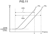
- FIG. 11 is a diagram illustrating an example of input and output characteristics of the current-to-voltage conversion unit 300 applicable to the first embodiment.
- a horizontal axis represents the photocurrent Iph output from the light receiving element 401a or 401b in logarithmic notation, and a vertical axis represents the output voltage Vp of the current-to-voltage conversion unit 300.
- FIG. 11 corresponds to a diagram in which the vertical axis and the horizontal axis of the graph of FIG. 10 are replaced.
- characteristic lines PD 1 and PD 2 illustrate a characteristic example of the low-sensitivity light receiving element 401a and a characteristic example of the normal-sensitivity light receiving element 401b described with reference to FIG. 5 , respectively.
- a dark current level is a voltage level obtained by converting dark currents generated in the light receiving elements 401a and 401b into voltages.
- the dark current level becomes a lower limit value of the output voltage Vp of the current-to-voltage conversion unit 300.
- the current value of the photocurrent Iph 1 output when the light having the same amount of light as that of the normal-sensitivity light receiving element 401b is incident on the low-sensitivity light receiving element 401a is smaller than the current value of the photocurrent Iph 2 output from the light receiving element 401b. That is, the photocurrent Iph 1 to be output is small even though a large amount of light is incident on the low-sensitivity light receiving element 401a.
- the characteristic line PD 1 of the light receiving element 401a shifts with respect to the characteristic line PD 2 of the light receiving element 401b in a direction in which the photocurrent Iph is large (rightward in FIG. 11 ).
- light detection for the address event detection is executed by using the low-sensitivity light receiving element 401a and the normal-sensitivity light receiving element 401b in combination. Accordingly, as illustrated in FIG. 11 , it is possible to extend a light detection range 420b using only the normal-sensitivity light receiving element 401b to a light detection range 420a including a light detection range using the low-sensitivity light receiving element 401a.
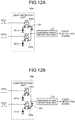
- FIGS. 12A and 12B are diagrams for describing control for detecting the address event by using the low-sensitivity light receiving element 401a and the normal-sensitivity light receiving element 401b according to the first embodiment.
- FIG. 12A illustrates an example in which the address event detection unit 30 detects the address event based on the photocurrent Iph 1 output from the light receiving element 401a.
- the signal OFG 1 supplied to the gate of the transistor 400a is set to the high state
- the signal OFG 2 supplied to the gate of the transistor 400b is set to the low state. Accordingly, the transistor 400a is turned on, the transistor 400b is turned off, and the photocurrent Iph 1 of the photocurrent Iph 1 output from the light receiving element 401a and the photocurrent Iph 2 output from the light receiving element 401b is supplied to the address event detection unit 30 through the transistor 400a.
- FIG. 12B illustrates an example in which the address event detection unit 30 detects the address event based on the photocurrent Iph 2 output from the light receiving element 401b.
- the signal OFG 1 supplied to the gate of the transistor 400a is set to the low state
- the signal OFG 2 supplied to the gate of the transistor 400b is set to the high state. Accordingly, the transistor 400a is turned off, the transistor 400b is turned on, and the photocurrent Iph 2 of the photocurrent Iph 1 output from the light receiving element 401a and the photocurrent Iph 2 output from the light receiving element 401b is supplied to the address event detection unit 30 through the transistor 400b.
- the address event detection unit 30 outputs the event detection signal based on a photocurrent Iph det of the photocurrents Iph 1 and Iph 2 selected according to the signals OFG 1 and OFG 2 .
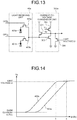
- FIG. 13 is a diagram illustrating an example of a configuration of a current-to-voltage conversion unit 300a to which the limiter is applied according to the first embodiment.
- the buffer amplifier 310, the subtraction unit 320, and the quantizer 330 in the address event detection unit 30 illustrated in FIG. 8 are omitted.
- the current-to-voltage conversion unit 300a has a configuration in which a transistor 304 which is a P-type MOS transistor is added as the limiter to the current-to-voltage conversion unit 300 of FIG. 8 . More specifically, a source of the transistor 304 is connected to an output path of an event detection signal of the current-to-voltage conversion unit 300a, that is, connection points between the drains of the transistors 302 and 303 and the gate of the transistor 301, and a drain of the transistor 304 is connected to the ground.
- an event detection signal of the current-to-voltage conversion unit 300a that is, connection points between the drains of the transistors 302 and 303 and the gate of the transistor 301, and a drain of the transistor 304 is connected to the ground.
- a predetermined limit voltage Lt is supplied to the gate of the transistor 304, and thus, an upper limit of the voltage value of the event detection signal output from the current-to-voltage conversion unit 300a can be limited to a voltage corresponding to the limit voltage Lt.
- the upper limit of the voltage value of the event detection signal output from the current-to-voltage conversion unit 300a is limited to the limit voltage Lt.
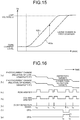
- FIG. 14 is a diagram illustrating an example of input and output characteristics of the current-to-voltage conversion unit 300a according to the first embodiment. Similar to FIG. 11 , a horizontal axis represents the photocurrent Iph output from the light receiving element 401a or 401b in logarithmic notation, and a vertical axis represents the output voltage Vp of the current-to-voltage conversion unit 300. As illustrated in FIG. 14 , the input and output characteristics of the current-to-voltage conversion unit 300a are characteristics obtained by limiting the output voltage Vp in the input and output characteristics of the current-to-voltage conversion unit 300 of FIG. 11 by the limit voltage Lt.
- the output voltage Vp based on the photocurrent Iph 1 of the low-sensitivity light receiving element 401a is limited to the limit voltage Lt at the current value a of the photocurrent Iph 1 using the light receiving element 401a corresponding to the voltage at the saturation point that shifts from the subthreshold region to the saturation region in the Id-Vg characteristics of the transistor 301.
- the output voltage Vp based on the photocurrent Iph 2 of the light receiving element 401b with normal sensitivity is also limited to the limit voltage Lt at the current value b of the photocurrent Iph 2 by the light receiving element 401b corresponding to the voltage at the saturation point.
- the photocurrent Iph det used for the address event detection is switched between the photocurrent Iph 1 output from the low-sensitivity light receiving element 401a and the photocurrent Iph 2 output from the normal-sensitivity light receiving element 401b by using a mechanism of the address event detection processing.
- the switching processing according to the first embodiment will be described with reference to FIGS. 15 to 18 .
- the signal OFG 1 is in the high state as an initial state and the photocurrent Iph 1 output from the low-sensitivity light receiving element 401a is supplied to the address event detection unit 30a.
- FIG. 15 is a diagram illustrating an example of the change in the photocurrent Iph 1 output from the low-sensitivity light receiving element 401a.
- both ends of the change in the photocurrent Iph 1 do not reach both ends of the detection range defined by the dark current level and the limit voltage Lt.
- These charts (a 1 ) and (b 1 ) relatively illustrate the changes in the photocurrents Iph 1 and Iph 2 .
- Relative changes in the amount of light received by the low-sensitivity PD and the amount of light received by the normal-sensitivity PD correspond to each other, and the change in the photocurrent Iph 1 of the low-sensitivity PD and the change in the photocurrent Iph 2 of the normal-sensitivity PD are relatively equal as illustrated in the charts (a 1 ) and (b 1 ).
- absolute values of the photocurrent Iph 1 and the photocurrent Iph 2 at the same timing are different, and, for example, the absolute value of the photocurrent Iph 2 is larger than the absolute value of the photocurrent Iph 1 .
- a chart (e 1 ) illustrates an example of the event detection signal output from the address event detection unit 30a.
- the event detection signal corresponding to the change in the photocurrent Iph 1 of the low-sensitivity PD illustrated in the chart (a 1 ) is output at points in time t 10 , t 11 , and t 12 .
- Charts (c 1 ) and (d 1 ) illustrate examples of arbitration for the event detection signal output from the pixel 20a including the low-sensitivity PD and the normal-sensitivity PD in the row arbiter 112 and the column arbiter 111, respectively.
- the event detection signal illustrated in the chart (e 1 ) is selected in the high state.
- charts (f 1 ) and (g 1 ) illustrate states of the signals OFG 1 and OFG 2 , respectively. Initially, the signal OFG 1 is in the high state, the signal OFG 2 is in the low state, and the photocurrent Iph 1 output from the low-sensitivity PD illustrated in the chart (a 1 ) is supplied to the address event detection unit 30.
- the control unit 115 acquires the event detection signal from the column arbiter 111, and predicts the photocurrent Iph 1 in the low-sensitivity PD and the amount of change in the photocurrent Iph 1 based on the acquired event detection signal.
- the control unit 115 switches the signal OFG 1 to the low state and the signal OFG 2 to the high state (point in time t 13 ). Accordingly, the photocurrent Iph 2 of the normal-sensitivity PD is supplied to the address event detection unit 30.
- the address event detection unit 30 obtains, as the amount of change in the photocurrent Iph, a result obtained by comparing the photocurrent Iph 1 of the low-sensitivity PD immediately before the signals OFG 1 and OFG 2 are switched at the point in time t 13 with the photocurrent Iph 2 of the normal-sensitivity PD in a state in which the signals OFG 1 and OFG 2 are switched at the point in time t 13 .
- the address event detection unit 30 detects the down event when the amount of change exceeds the OFF threshold value in the positive direction, and detects the up event when the amount of change exceeds the ON threshold value in the negative direction (see FIG. 9 ).
- the address event detection unit 30 detects the up event when the amount of change exceeds the OFF threshold value in the positive direction, and outputs the event detection signal (point in time t 14 ).
- the column arbiter 111 and the row arbiter 112 select the event detection signal at this point in time t 14 .
- the control unit 115 returns the signal OFG 1 to the high state (point in time t 15 ), and returns the signal OFG 2 to the low state (point in time t 16 ). Thereafter, the address event detection unit 30 detects the address event by continuously using the low-sensitivity PD selected in the initial state (for example, point in time t 17 ).
- FIG. 17 is a diagram corresponding to FIG. 15 and illustrates an example of the change in the photocurrent Iph 1 output from the low-sensitivity light receiving element 401a.
- a lower end of the change in the photocurrent Iph 1 reaches the dark current level.
- the amount of change in the amount of light that causes the change in the photocurrent Iph 1 may be larger than the amount of change in the amount of light indicated by the amount of change in the photocurrent Iph 1 .
- FIG. 18 is a timing chart illustrating an example of processing in the solid-state imaging device 11a corresponding to the change in the photocurrent Iph 1 of FIG. 17 . Since the meanings of the charts (a 2 ) to (g 2 ) in FIG. 18 are the same as those of the charts (a 1 ) to (g 1 ) in FIG. 16 , the description thereof is omitted here. As in the case of FIG. 16 , in the example of FIG. 18 , the event detection signal corresponding to the change in the photocurrent Iph 1 of the low-sensitivity PD is output at points in time t 20 , t 21 , and t 22 as illustrated in the chart (e 2 ).
- the signal OFG 1 is initially in the high state, the signal OFG 2 is in the low state, and the photocurrent Iph 1 output from the low-sensitivity PD illustrated in the chart (a 2 ) is supplied to the address event detection unit 30 as illustrated in charts (f 2 ) and (g 2 ).
- the control unit 115 predicts the photocurrent Iph 1 in the low-sensitivity PD and the amount of change in the photocurrent Iph 1 based on the event detection signal acquired from the column arbiter 111 as in the description of FIG. 16 .
- the control unit 115 switches the signal OFG 1 to the low state and the signal OFG 2 to the high state (point in time t 23 ). Accordingly, the photocurrent Iph 2 of the normal-sensitivity PD is supplied to the address event detection unit 30.
- the column arbiter 111 and the row arbiter 112 select the event detection signal at this point in time t 24 .
- the control unit 115 maintains the low state of the signal OFG 1 and the high state of the signal OFG 2 even though this event detection signal is acquired from the column arbiter 111, and performs the address event detection by using the normal-sensitivity PD switched from the low-sensitivity PD at the point in time t 23 .
- the first embodiment it is possible to execute control for switching the photocurrent Iph det used for the address event detection between the photocurrent Iph 1 output from the low-sensitivity PD (light receiving element 401a) and the photocurrent Iph 2 output from the normal-sensitivity PD (light receiving element 401b) by using the configuration for detecting the address event.
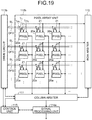
- a drive circuit 113b generates the signal OFG in units of rows under the control of the control unit 115, and supplies the generated signal OFG to each pixel 20a via a common terminal Tc of the switch 21 connected to each pixel 20a.
- the switch 21 selects any one of the terminals Tm 1 and Tm 2 according to a selection signal SL supplied from the drive circuit 113b.
- the drive circuit 113b generates each selection signal SL corresponding to each pixel 20a under the control of the control unit 115, and supplies the selection signal to the switch 21 connected to each pixel 20a for each row.
- FIG. 19 illustrates that a plurality of selection signals SL is supplied as the selection signals SL.
- the selected states of the terminals Tm 1 and Tm 2 in each switch 21 corresponding to a certain selection signal SL are maintained until the next selection signal SL is supplied. Accordingly, in each pixel 20a, the selected state of the photocurrent Iph 1 using the low-sensitivity light receiving element 401a and the photocurrent Iph 2 using the normal-sensitivity light receiving element 401b can be maintained.
- the switch 21 is provided outside the pixel 20a
- the present invention is not limited to this example, and the switch 21 may be provided inside the pixel 20a.
- the selection signal SL is supplied to each pixel 20a
- the present invention is not limited to this example.
- a logic circuit that switches between the terminals Tm 1 and Tm 2 of the switch 21 according to a specific bit string may be provided so as to correspond to each pixel 20a. By doing so, it is possible to reduce the number of signal lines for supplying the selection signals SL.
- one switch 21 is connected to one pixel 20a
- the present invention is not limited to this example, and one switch 21 can be shared by a plurality of pixels 20a.
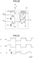
- FIG. 20 is a diagram illustrating a configuration of an example of a pixel 20b according to the second embodiment.
- the pixel 20b includes a light receiving unit 40b and the current-to-voltage conversion unit 300.
- the current-to-voltage conversion unit 300 has the same configuration as the current-to-voltage conversion unit 300 described with reference to FIG. 8 , and thus, the description thereof is omitted here.
- the limiter (transistor 304) described with reference to FIG. 13 may be added to the current-to-voltage conversion unit 300 of FIG. 20 .
- the light receiving unit 40b includes light receiving elements 401c and 401d having substantially the same sensitivity. Similar to the configuration of FIG. 5 , in the light receiving element 401c, a cathode is connected to the ground, and an anode is connected to the source of the transistor 400a which is the N-type MOS transistor. The drain of the transistor 400a is connected to the connection point at which the source of the transistor 301 and the gate of the transistor 303 of the current-to-voltage conversion unit 300 are connected. The signal OFG 1 is supplied to the gate of the transistor 400a.
- FIG. 21 is a time chart illustrating an example of a method of driving the light receiving unit 40b according to the second embodiment.
- charts (h) and (i) illustrate states of the signals OFG 1 and OFG2, respectively, and a chart (j) illustrates an output voltage Vp output from the current-to-voltage conversion unit 300.
- the control unit 115 acquires the output voltage Vp output from the current-to-voltage conversion unit 300 in synchronization with this switching timing, compares an output voltage Vp 1 when the signal OFG 1 is in the high state with an output voltage Vp 2 when the signal OFG 2 is in the high state, and obtains a difference 406 between the output voltages Vp 1 and Vp 2 .
- This processing corresponds to the processing of obtaining the difference between the photocurrent Iph 1 output from the light receiving element 401c and the photocurrent Iph 2 output from the light receiving element 401d.
- the control unit 115 handles this difference 406 as the event detection signal, and analyzes this difference in the control unit 115 or outside.
- FIGS. 22A, 22B, and 22C are diagrams illustrating an example of the configuration of the light receiving elements 401c and 401d applicable to the second embodiment.
- FIG. 22A illustrates an example of a pixel 20b(a) in which the light receiving elements 401c and 401d are arranged in parallel.
- information regarding an edge of the image can be acquired based on the difference 406.
- FIG. 22B illustrates an example of a pixel 20b(b) in which the light receiving elements 401c and 401d are arranged in parallel and adjacent to each other, and adjacent portions of the light receiving elements 401c and 401d are shielded by using a light shielding pattern 407.
- the light shielding pattern 407 is, for example, a metal light shielding pattern.
- the light incident on the pixel 20b(b) is received by the light receiving elements 401c and 401d through openings which are not shielded by the light shielding pattern 407.
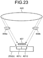
- FIG. 23 is a schematic diagram illustrating a scene in which the light is incident on the light receiving elements 401c and 401d in the pixel 20b(b) of FIG. 22B .
- the light shielding pattern 407 is provided on the light receiving elements 401c and 401d arranged adjacent to each other, and a lens 440 is provided so as to correspond to the pixel 20b(b).
- the lens 440 is, for example, an On Chip Lense (OCL).
- the pixel 20b(b) is irradiated with the light incident on the lens 440. However, this light is shielded by the light shielding pattern 407, and is not incident on a right side of the light receiving element 401c and a left side of the light receiving element 401d in FIG. 23 .
- Light 409a on the left side of the lens 440 in FIG. 23 is incident on the unshielded left side of the light receiving element 401c.
- Light 409b on the right side is incident on the unshielded right side of the light receiving element 401d.
- the pixel 20b(b) can be utilized as an image plane phase difference pixel.
- the image plane phase difference pixel includes, for example, a set of two pixels of a pixel in which an opening filter having an opening on a left half region of the light receiving surface of the light receiving element is stacked and a pixel in which an opening filter having an opening on a right half region of the light receiving surface of another light receiving element is stacked. A distance is measured based on a phase difference between light rays received by the two pixels. Due to the use of the configuration of FIG. 22B , it is possible to form the image plane phase difference pixel by one pixel 20b(b).
- FIG. 22C illustrates an example of the pixel 20b(c) in which polarization filters 408 are provided for the light receiving elements 401c and 401d in different polarization directions.
- the polarization filter 408 can be formed by the metal light shielding pattern in which a large number of slits for transmitting light are provided in parallel. As stated above, it is possible to detect polarization by one pixel 20b(c) by setting the polarization directions of the light receiving elements 401c and 401d included in the pixel 20b(c) to be different.
- the control unit 115 acquires the output voltage Vp 1 obtained by converting the photocurrent Iph output from the light receiving element 401c when the signal OFG 1 shifts from the high state to the low state.
- the signal OFG 1 shifts the low state
- the signal OFG 2 shifts the high state.
- the control unit 115 acquires the output voltage Vp 2 obtained by converting the photocurrent Iph output from the light receiving element 401d. It is assumed that the control unit 115 obtains the difference 406 between the output voltages Vp 1 and Vp 2 and detects the address event when the difference 406 exceeds the ON threshold value or the OFF threshold value in a predetermined direction.
- the pixel 20b including the light receiving elements 401c and 401d having the same sensitivity can be utilized for various purposes.
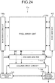
- each pixel includes the plurality of light receiving elements that outputs the photocurrents Iph corresponding to the received light rays, the address event detection unit that detects the address event based on the amount of changes in the photocurrents Iph output from the plurality of light receiving elements, and a pixel signal generation unit that generates pixel signals that are analog signals of voltages corresponding to the absolute value of the photocurrents Iph.
- the row drive circuit 113c has a function of driving each pixel and outputting the pixel signal to the column drive circuit 116 in addition to the function of the drive circuit 113a of FIG. 2 .
- the column drive circuit 116 includes an analog to digital (AD) converter for each column, and a drive circuit that scans the AD converter for each column in the row direction.
- the AD converter for each column is called a column AD converter (ADC).
- the column drive circuit 116 outputs the pixel signals converted into digital signals by the AD converters in units of rows by scanning the column ADC in the row direction.
- the pixel signal output from the column drive circuit 116 is supplied to the signal processing unit 114c.
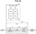
- FIG. 25 is a block diagram illustrating a configuration of an example of the pixel array unit 110c according to the third embodiment.
- the pixel array unit 110c includes a plurality of pixels 20c arrayed in a two-dimensional lattice.
- each pixel 20c includes the address event detection unit 30, a light receiving unit 40c, and a pixel signal generation unit 41.
- the light receiving unit 40c includes a plurality of light receiving elements, photoelectrically converts incident light, and generates the photocurrent Iph.
- the light receiving unit 40c supplies the generated photocurrent Iph to any of the pixel signal generation unit 41 and the address event detection unit 30 under the control of the row drive circuit 113c.
- the address event detection unit 30 includes the current-to-voltage conversion unit 300a described with reference to FIG. 13 that limits the upper limit of the output voltage Vp to the limit voltage Lt by the limiter.
- the pixel signal generation unit 41 generates, as the pixel signal, a signal having a voltage corresponding to the photocurrent Iph supplied from the light receiving unit 40c.
- the pixel signal generation unit 41 supplies the generated pixel signal to the column drive circuit 116 via a vertical signal line.
- FIG. 26 is a diagram illustrating a configuration of an example of the pixel 20c according to the third embodiment.
- the light receiving unit 40c includes two light receiving elements 401a and 401b which are, for example, photodiodes, and transistors 400a, 400b, 402a and 402b which are N-type MOS transistors.
- the pixel signal generation unit 41 includes a floating diffusion layer 413, and a reset transistor 410, an amplification transistor 411, and a selection transistor 412 which are N-type MOS transistors, respectively.
- a signal OFG 1 is supplied to a gate of the transistor 400a.
- the transistor 400a is turned on when the signal OFG 1 is in the high state, and is turned off when the signal OFG 1 is in the low state.
- a signal OFG 2 is supplied to a gate of the transistor 400b.
- the transistor 400b is turned on when the signal OFG 2 is in the high state, and is turned off when the signal OFG 2 is in the low state.
- a photocurrent Iph 1 output from the light receiving element 401a is supplied to the address event detection unit 30.
- a photocurrent Iph 2 output from the light receiving element 401b is supplied to the address event detection unit 30.
- a signal TRG 1 is supplied to a gate of the transistor 402a.
- the transistor 402a is turned on when the signal TRG 1 is in the high state, and is turned off when the signal OFG 1 is in the low state.
- a signal TRG 2 is supplied to a gate of the transistor 402b.
- the transistor 402b is turned on when the signal TRG 2 is in the high state, and is turned off when the signal TRG 2 is in the low state.
- the photocurrent Iph 1 output from the light receiving element 401a is supplied to the pixel signal generation unit 41.
- the photocurrent Iph 2 output from the light receiving element 401b is supplied to the pixel signal generation unit 41.
- the floating diffusion layer 413 accumulates charges, and generates a voltage according to the amount of accumulated charges.
- the reset transistor 410 initializes the amount of charges of the floating diffusion layer 413 according to a reset signal RST supplied from the row drive circuit 113c.
- the amplification transistor 411 amplifies the voltage of the floating diffusion layer 413.
- the selection transistor 412 outputs, as a pixel signal SIG, a signal of a voltage amplified by the amplification transistor 411 to the column drive circuit 116 via a vertical signal line VSL according to a selection signal SEL from the row drive circuit 113c.
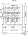
- FIG. 27 is a schematic diagram illustrating an example of wirings in the pixel array unit 110c according to the third embodiment. Similar to the drive circuit 113a of the pixel array unit 110a according to the first embodiment described with reference to FIG. 7 , the row drive circuit 113c generates the signals OFG 1 and OFG 2 under the control of the control unit 115, and the generated signals OFG 1 and OFG 2 are supplied to each pixel 20c. In the example of FIG. 27 , the row drive circuit 113c generates the signals OFG 1 and OFG 2 for each row for each pixel 20c arrayed in a two-dimensional lattice in the pixel array unit 110c.
- the row drive circuit 113c further generates the signals TRG 1 and TRG 2 under the control of the control unit 115, and supplies the generated signals TRG 1 and TRG 2 to each pixel 20c.
- the row drive circuit 113c generates the signals TRG 1 and TRG 2 for each row for each pixel 20c arrayed in a two-dimensional lattice in the pixel array unit 110c.
- the vertical signal line VSL of each pixel 20c is connected to the column drive circuit 116 for each column of each pixel 20c arrayed in the pixel array unit 110c.
- the row drive circuit 113c further generates the reset signal RST and the selection signal SEL for each of the pixels 20c arrayed in the two-dimensional lattice in the pixel array unit 110c under the control of the control unit 115 for each row.
- the row drive circuit 113c supplies the generated reset signal RST and selection signal SEL to each pixel 20c.
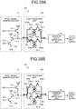
- FIGS. 28A and 28B are diagrams for describing the control of the light receiving unit 40c according to the third embodiment.
- FIG. 28A illustrates an example in which the address event is detected by the address event detection unit 30 based on the photocurrent Iph 1 output from the light receiving element 401a which is the low-sensitivity PD.
- the signal OFG 1 supplied to the gate of the transistor 400a is set to the high state
- the signal OFG 2 supplied to the gate of the transistor 400b is set to the low state
- the signal TRG 1 supplied to the gate of the transistor 402a is set to the low state
- the signal TRG 2 supplied to the gate of the transistor 402b is set to the high state.
- the transistor 400a is turned on, the transistor 400b is turned off, the transistor 402a is turned off, and the transistor 402b is turned on.
- the photocurrent Iph 1 of the photocurrent Iph 1 output from the light receiving element 401a which is the low-sensitivity PD and the photocurrent Iph 2 output from the light receiving element 401b which is the normal-sensitivity PD is supplied to the address event detection unit 30 via the transistor 400a, and the photocurrent Iph 2 is supplied to the pixel signal generation unit 41 via the transistor 402b.
- FIG. 28B illustrates an example in which the address event detection unit 30 detects the address event based on the photocurrent Iph 2 output from the light receiving element 401b which is the normal-sensitivity PD.
- the signal OFG 1 supplied to the gate of the transistor 400a is set to the low state
- the signal OFG 2 supplied to the gate of the transistor 400b is set to the high state
- the signal TRG 1 supplied to the gate of the transistor 402a is set to the high state
- the signal TRG 2 supplied to the gate of the transistor 402b is set to the low state.
- the transistor 400a is turned off, the transistor 400b is turned on, the transistor 402a is turned on, and the transistor 402b is turned off.
- the photocurrent Iph 1 of the photocurrent Iph 1 output from the light receiving element 401a which is the low-sensitivity PD and the photocurrent Iph 2 output from the light receiving element 401b which is the normal-sensitivity PD is supplied to the address event detection unit 30 via the transistor 400b, and the photocurrent Iph 2 is supplied to the pixel signal generation unit 41 via the transistor 402a.
- FIG. 29 is a timing chart illustrating an example of processing in the solid-state imaging device 11c according to the third embodiment.
- charts (k) and (n) illustrate examples of the reset signal RST and the selection signal SEL generated in the row drive circuit 113c.
- a chart (o) illustrates an example of the voltage of the pixel signal in the vertical signal line VSL.
- charts (1) and (m) illustrate examples of the signals TRG 1 and TRG 2 generated in the row drive circuit 113c
- charts (s) and (t) illustrate examples of the signals OFG 1 and OFG 2 generated in the row drive circuit 113c.
- a chart (r) illustrates an example of the event detection signal output from the address event detection unit 30.
- Charts (p) and (q) illustrate examples of arbitration for the event detection signal illustrated in the chart (r) in the row arbiter 112 and the column arbiter 111, respectively.
- the event detection signal illustrated in the chart (r) is selected in the high state.
- the signal OFG 1 is in the high state and the signal OFG 2 is in the low state as an initial state, and the photocurrent Iph 1 output from the low-sensitivity PD is supplied to the address event detection unit 30.
- the amount of change in the photocurrent Iph 1 in the low-sensitivity PD exceeds a predetermined amount, and the event detection signal is output from the address event detection unit 30 at a point in time t 30 .
- the control unit 115 acquires this event detection signal from the column arbiter 111, and instructs the row drive circuit 113c to set the signal OFG 1 to the low state according to the acquired event detection signal.
- the row drive circuit 113c sets the signal OFG 1 to the low state according to this instruction (point in time t 31 ).
- the row drive circuit 113c sets the reset signal RST and the signal TRG 1 to the high state, and resets the low-sensitivity PD (light receiving element 401a) and the floating diffusion layer 413.
- the row drive circuit 113c sets the reset signal RST and the signal TRG 2 to the high state, and resets the normal-sensitivity PD (light receiving element 401b) and the floating diffusion layer 413.
- a period 510 including the points in point in time t 40 and t 41 is an exposure start sequence in a voltage read operation of the pixel signal SIG.
- the selection signal SEL since the selection signal SEL is maintained in the low state, the pixel signal SIG is not output to the vertical signal line VSL.
- the row drive circuit 113c sets the selection signal SEL to the high state, and starts outputting the pixel signal SIG to the vertical signal line VSL.
- the row drive circuit 113c maintains the high state of the selection signal SEL until a point in time t 49 at which CDS reading using the normal-sensitivity PD (light receiving element 401b) is ended.
- the row drive circuit 113c sets the reset signal RST to the high state at a point in time t 44 immediately after the point in time t 42 , and sets the signal TRG 1 to the high state at a point in time t 45 .
- a pixel signal SIG 1 based on the photocurrent Iph 1 output from the low-sensitivity PD (light receiving element 401a) is supplied to the column drive circuit 116 via the vertical signal line VSL, and the CDS reading of the low-sensitivity PD is performed (period 511a).
- the row drive circuit 113c sets the reset signal RST to the high state at a point in time t 47 immediately after a point in time t 46 at which the CDS reading of the low-sensitivity PD is ended, and sets the signal TRG 2 to the high state at a point in time t 48 .
- Ae pixel signal SIG 2 based on the photocurrent Iph 2 output from the normal-sensitivity PD (light receiving element 401b) is supplied to the column drive circuit 116 via the vertical signal line VSL, and the CDS reading of the normal-sensitivity PD is performed (period 511b).
- a period 511 including the periods 511a and 511b is a reading sequence in the voltage read operation of the pixel signal SIG.
- a time 520a from the point in time t 40 at which the signal TRG 1 is in the high state in the period 510 to the point in time t 44 at which the signal TRG 1 is in the high state in the period 511 and a time 520b from the point in time t 41 at which the signal TRG 2 is in the high state in the period 510 to the point in time t 48 at which the signal TRG 2 is in the high state in the period 511 is set to be equal, and an exposure time of the low-sensitivity PD (light receiving element 401a) and an exposure time of the normal-sensitivity PD (light receiving element 401b) are aligned.
- the row drive circuit 113c sets the selection signal SEL to the low state, and stops outputting the pixel signal SIG from the pixel signal generation unit 41.
- the control unit 115 acquires the pixel signal SIG 1 read in the period 511a and the pixel signal SIG 2 read in the period 511b from the column drive circuit 116.
- the control unit 115 selects the photocurrent Iph det used for the address event detection in the address event detection unit 30 of the photocurrent Iph 1 of the low-sensitivity PD (light receiving element 401a) and the photocurrent Iph 2 of the normal-sensitivity PD (light receiving element 401b) based on the acquired pixel signals SIG 1 and SIG 2 .
- control unit 115 selects, as the photocurrent Iph det used for the address event detection in the address event detection unit 30, the photocurrent Iph 2 of the normal-sensitivity PD.
- the row drive circuit 113c sets the signal OFG 1 to the low state and the signal OFG 2 to the high state, and supplies the photocurrent Iph 2 output from the normal-sensitivity PD (light receiving element 401b) to the address event detection unit 30.
- control unit 115 sets a timing at which the address event detection unit 30 executes the address event detection (indicated by a dotted frame in FIG. 29 ) to be fixed, and performs control such that the address event detection using the address event detection unit 30 is executed at constant cycles. That is, one cycle of the execution of the address event detection includes a pixel signal read operation in the periods 510 and 511, and an address event detection based on the read operation.
- FIGS. 30 and 31 are diagrams for describing a method of switching between the low-sensitivity PD and the normal-sensitivity PD based on a voltage difference according to the third embodiment.
- FIGS. 30 and 31 are diagrams corresponding to FIG. 14 .
- the meanings of the horizontal axis and the vertical axis and the characteristic lines 403a and 403b are common to FIG. 14 , and thus, the description thereof is omitted here.
- FIG. 30 illustrates an example of an operation of switching the photocurrent Iph det used by the address event detection unit 30 to the photocurrent Iph 1 output from the low-sensitivity PD (light receiving element 401a) from the photocurrent Iph 2 output from the normal-sensitivity PD (light receiving element 401b) when the amount of light is increased.
- the control unit 115 determines whether or not the output voltage Vp of the current-to-voltage conversion unit 300a included in the address event detection unit 30 falls in a limit region of the limit voltage Lt. For example, when it is determined that the output voltage Vp falls in the limit region in step S11, the control unit 115 switches the photocurrent Iph det used for address event detection by the address event detection unit 30 to the photocurrent Iph 1 of the low-sensitivity PD in synchronization with the detection of the up event using the address event detection unit 30, and acquires the output voltage Vp.
- the control unit 115 compares the acquired output voltage Vp (referred to as a voltage Vp low ) of the photocurrent Iph 1 of the low-sensitivity PD with the output voltage Vp (referred to as a voltage Vp nml ) used for the determination in step S11. As the comparison result, when a difference between the voltage Vp low and the voltage Vp nml is equal to or less than a predetermined value, the control unit 115 sets the signal OFG 1 to the high state and the signal OFG 2 to the low state, and switches the photocurrent Iph det used for the address event detection by the address event detection unit 30 from the photocurrent Iph 2 to the photocurrent Iph 1 (step S12).
- FIG. 31 illustrates an example of an operation of switching the photocurrent Iph det used by the address event detection unit 30 from the photocurrent Iph 1 output by the low-sensitivity PD (light receiving element 401a) to the photocurrent Iph 2 output by the normal-sensitivity PD (light receiving element 401b) when the amount of light is decreased.
- step S20 a decrease in the amount of light received by the pixel 20c is detected based on, for example, the pixel signal SIG read in the period 511 in FIG. 29 .
- the control unit 115 determines whether or not the output voltage Vp of the current-to-voltage conversion unit 300a included in the address event detection unit 30 falls in a dark current region of the dark current level. For example, when it is determined that the output voltage Vp falls in the dark current region in step S21, the control unit 115 switches the photocurrent Iph det used for the address event detection by the address event detection unit 30 in synchronization with the detection of the down event using the address event detection unit 30 to the photocurrent Iph 2 of the normal-sensitivity PD, and acquires the output voltage Vp.
- the control unit 115 compares the acquired output voltage Vp (voltage Vp nml ) of the photocurrent Iph 2 of the normal-sensitivity PD with the output voltage Vp (voltage Vp low ) used for the determination in step S21. As the comparison result, when a difference between the voltage Vp nml and the voltage Vp low is equal to or less than a predetermined value, the control unit 115 sets the signal OFG 1 to the low state and the signal OFG 2 to the high state, and switches the photocurrent Iph det used for the address event detection by the address event detection unit 30 from the photocurrent Iph 1 to the photocurrent Iph 2 (step S22).
- FIG. 32 is a flowchart of an example of an operation of switching the photocurrent Iph when the amount of light received by the pixel 20c is increased according to the third embodiment described with reference to FIG. 30 .
- the signal OFG 1 is in the low state
- the signal OFG 2 is in the high state
- the photocurrent Iph 2 of the normal-sensitivity PD is selected as the photocurrent Iph det used for the address event detection by the address event detection unit 30.
- step S101 the control unit 115 determines whether or not the output voltage Vp (voltage Vp nml ) of the current-to-voltage conversion unit 300a falls in the limit region.
- step S101 the processing returns to step S100, for example.
- step S101 the processing proceeds to step S102.
- step S102 the control unit 115 acquires the voltage Vp nml based on the photocurrent Iph 2 of the normal-sensitivity PD.
- step S103 the control unit 115 sets the signal OFG 1 to the high state and the signal OFG 2 to the low state, and switches the photocurrent Iph supplied to the address event detection unit 30 to the photocurrent Iph 1 of the low-sensitivity PD.
- step S104 the control unit 115 acquires the voltage Vp low based on the photocurrent Iph 1 of the low-sensitivity PD.
- control unit 115 detects the difference between the voltage Vp nml obtained in step S102 and the voltage Vp low acquired in step S104 in synchronization with the up event detected based on the photocurrent Iph 2 of the normal-sensitivity PD during the period of step S100 and step S101.
- control unit 115 determines whether or not the difference detected in step S105 is equal to or less than a predetermined value.
- the control unit 115 determines that the difference is equal to or less than the predetermined value (step S106, "Yes"), the processing proceeds to step S107.
- the control unit 115 sets the signal OFG 1 to the high state and the signal OFG 2 to the low state, and selects, as the photocurrent Iph det used for the address event detection by the address event detection unit 30, the photocurrent Iph 1 of the low-sensitivity PD.
- step S106 determines in step S106 that the difference exceeds the predetermined value (step S106, "No")
- the processing proceeds to step S108.
- step S108 the control unit 115 maintains the states of the signals OFG 1 and OFG 2 , and selects, as the photocurrent Iph det used for the address event detection by the address event detection unit 30, the photocurrent Iph 2 of the normal-sensitivity PD.
- step S107 or step S108 When the processing of step S107 or step S108 is ended, the series of processing according to the flowchart of FIG. 32 is ended.
- FIG. 33 is a flowchart of an example of an operation of switching the photocurrent Iph when the amount of light received by the pixel 20c is decreased according to the third embodiment described with reference to FIG. 31 .
- the signal OFG 1 is in the high state
- the signal OFG 2 is in the low state
- the photocurrent Iph 1 of the low-sensitivity PD is selected as the photocurrent Iph det used for the address event detection by the address event detection unit 30.
- step S200 the control unit 115 determines whether or not the amount of light received by the pixel 20c is decreased based on the pixel signal SIG.
- step S200 determines that the amount of light is not decreased (step S200, "No")
- step S200 determines that the amount of light is not decreased (step S200, "No")
- step S200 determines that the amount of light received by the pixel 20c is decreased (step S200, "Yes")
- the processing proceeds to step S201.
- step S201 the control unit 115 determines whether or not the output voltage Vp (voltage Vp low ) of the current-to-voltage conversion unit 300a falls in the dark current region.
- step S201 the processing returns to step S200, for example.
- step S201 the processing proceeds to step S202.
- step S202 the control unit 115 acquires the voltage Vp low8 based on the photocurrent Iph 1 of the low-sensitivity PD.
- step S203 the control unit 115 sets the signal OFG 1 to the low state and the signal OFG 2 to the high state, and switches the photocurrent Iph supplied to the address event detection unit 30 to the photocurrent Iph 2 of the normal-sensitivity PD.
- step S204 the control unit 115 acquires the voltage Vp nml based on the photocurrent Iph 2 of the normal-sensitivity PD.
- step S206 the control unit 115 determines whether or not the difference detected in step S205 is equal to or less than a predetermined value.
- step S206 the control unit 115 determines that the difference is equal to or less than the predetermined value (step S206, "Yes")
- step S207 the control unit 115 sets the signal OFG 1 to the low state and the signal OFG 2 to the high state, and selects, as the photocurrent Iph det used for the address event detection by the address event detection unit 30, the photocurrent Iph 2 of the normal-sensitivity PD.
- step S207 or step S208 When the processing of step S207 or step S208 is ended, the series of processing according to the flowchart of FIG. 33 is ended.
- the amount of light received by the pixel 20c is determined based on the pixel signal SIG, and the photocurrent Iph det used for the address event detection by the address event detection unit 30 is selected from the photocurrents Iph 1 and Iph 2 based on the determination result.
- the processing of selecting the photocurrent Iph det from the photocurrents Iph 1 and Iph 2 can be executed with higher accuracy.
Landscapes
- Engineering & Computer Science (AREA)
- Multimedia (AREA)
- Signal Processing (AREA)
- Transforming Light Signals Into Electric Signals (AREA)
- Solid State Image Pick-Up Elements (AREA)
- Light Receiving Elements (AREA)
Applications Claiming Priority (2)
| Application Number | Priority Date | Filing Date | Title |
|---|---|---|---|
| JP2018186127A JP2022002355A (ja) | 2018-09-28 | 2018-09-28 | 固体撮像素子、固体撮像素子の制御方法および電子機器 |
| PCT/JP2019/033616 WO2020066433A1 (fr) | 2018-09-28 | 2019-08-28 | Élément d'imagerie à semi-conducteurs, procédé de commande d'élément d'imagerie à semi-conducteurs et appareil électronique |
Publications (3)
| Publication Number | Publication Date |
|---|---|
| EP3860115A1 true EP3860115A1 (fr) | 2021-08-04 |
| EP3860115A4 EP3860115A4 (fr) | 2021-11-24 |
| EP3860115B1 EP3860115B1 (fr) | 2025-04-02 |
Family
ID=69951846
Family Applications (1)
| Application Number | Title | Priority Date | Filing Date |
|---|---|---|---|
| EP19864558.2A Active EP3860115B1 (fr) | 2018-09-28 | 2019-08-28 | Élément d'imagerie à semi-conducteurs, procédé de commande d'élément d'imagerie à semi-conducteurs et appareil électronique |
Country Status (6)
| Country | Link |
|---|---|
| US (1) | US11553151B2 (fr) |
| EP (1) | EP3860115B1 (fr) |
| JP (1) | JP2022002355A (fr) |
| KR (1) | KR20210069627A (fr) |
| CN (1) | CN112740661B (fr) |
| WO (1) | WO2020066433A1 (fr) |
Families Citing this family (11)
| Publication number | Priority date | Publication date | Assignee | Title |
|---|---|---|---|---|
| JP2021048554A (ja) * | 2019-09-20 | 2021-03-25 | ソニーセミコンダクタソリューションズ株式会社 | 撮像装置、撮像制御方法、プログラム |
| JP7660571B2 (ja) * | 2020-06-26 | 2025-04-11 | ソニーセミコンダクタソリューションズ株式会社 | 固体撮像装置 |
| US20230316693A1 (en) * | 2020-09-16 | 2023-10-05 | Sony Group Corporation | Solid-state imaging device and recognition system |
| JPWO2022215371A1 (fr) * | 2021-04-09 | 2022-10-13 | ||
| WO2023281724A1 (fr) | 2021-07-08 | 2023-01-12 | キヤノン株式会社 | Élément d'imagerie, dispositif d'imagerie, dispositif de surveillance et procédé de commande d'élément d'imagerie |
| TWI792651B (zh) * | 2021-11-01 | 2023-02-11 | 友達光電股份有限公司 | 感光裝置 |
| JP2023081054A (ja) * | 2021-11-30 | 2023-06-09 | ソニーセミコンダクタソリューションズ株式会社 | 半導体装置および信号処理方法、並びにプログラム |
| CN114500868B (zh) * | 2022-04-18 | 2022-07-12 | 深圳锐视智芯科技有限公司 | 一种evs像素工作方法及相关装置 |
| US20260052319A1 (en) * | 2022-09-21 | 2026-02-19 | Sony Semiconductor Solutions Corporation | Solid-state imaging device |
| CN121866777A (zh) * | 2023-10-30 | 2026-04-14 | 索尼半导体解决方案公司 | 信息处理装置、成像装置和程序 |
| WO2025205977A1 (fr) * | 2024-03-26 | 2025-10-02 | ソニーセミコンダクタソリューションズ株式会社 | Dispositif de détection de lumière |
Family Cites Families (12)
| Publication number | Priority date | Publication date | Assignee | Title |
|---|---|---|---|---|
| US7551059B2 (en) * | 2005-01-06 | 2009-06-23 | Goodrich Corporation | Hybrid infrared detector array and CMOS readout integrated circuit with improved dynamic range |
| JP6480862B2 (ja) | 2013-07-22 | 2019-03-13 | ソニーセミコンダクタソリューションズ株式会社 | 固体撮像素子および電子機器 |
| KR102054774B1 (ko) | 2013-09-10 | 2019-12-11 | 삼성전자주식회사 | 동적 비전 센서, 조도 센서, 및 근접 센서 기능을 구비한 이미지 장치 |
| JP6577700B2 (ja) * | 2014-06-30 | 2019-09-18 | キヤノン株式会社 | 放射線検出装置、その制御方法、放射線撮影装置、およびプログラム |
| US9986179B2 (en) | 2014-09-30 | 2018-05-29 | Qualcomm Incorporated | Sensor architecture using frame-based and event-based hybrid scheme |
| JP2016092661A (ja) * | 2014-11-07 | 2016-05-23 | ソニー株式会社 | 撮像素子および駆動方法、並びに電子機器 |
| JP6754157B2 (ja) | 2015-10-26 | 2020-09-09 | ソニーセミコンダクタソリューションズ株式会社 | 撮像装置 |
| US11280918B2 (en) * | 2015-12-16 | 2022-03-22 | Sony Corporation | Imaging element, driving method, and electronic device |
| KR102612194B1 (ko) * | 2016-12-14 | 2023-12-11 | 삼성전자주식회사 | 이벤트 기반 센서 및 이벤트 기반 센싱 방법 |
| US10516841B2 (en) * | 2017-03-08 | 2019-12-24 | Samsung Electronics Co., Ltd. | Pixel, pixel driving circuit, and vision sensor including the same |
| JP6696695B2 (ja) * | 2017-03-16 | 2020-05-20 | 株式会社東芝 | 光検出装置およびこれを用いた被写体検知システム |
| US11140349B2 (en) * | 2018-09-07 | 2021-10-05 | Samsung Electronics Co., Ltd. | Image sensor incuding CMOS image sensor pixel and dynamic vision sensor pixel |
-
2018
- 2018-09-28 JP JP2018186127A patent/JP2022002355A/ja active Pending
-
2019
- 2019-08-28 EP EP19864558.2A patent/EP3860115B1/fr active Active
- 2019-08-28 KR KR1020217006265A patent/KR20210069627A/ko active Pending
- 2019-08-28 US US17/277,286 patent/US11553151B2/en active Active
- 2019-08-28 CN CN201980061529.5A patent/CN112740661B/zh active Active
- 2019-08-28 WO PCT/JP2019/033616 patent/WO2020066433A1/fr not_active Ceased
Also Published As
| Publication number | Publication date |
|---|---|
| US11553151B2 (en) | 2023-01-10 |
| CN112740661A (zh) | 2021-04-30 |
| US20220030190A1 (en) | 2022-01-27 |
| KR20210069627A (ko) | 2021-06-11 |
| CN112740661B (zh) | 2024-09-13 |
| JP2022002355A (ja) | 2022-01-06 |
| EP3860115A4 (fr) | 2021-11-24 |
| WO2020066433A1 (fr) | 2020-04-02 |
| EP3860115B1 (fr) | 2025-04-02 |
Similar Documents
| Publication | Publication Date | Title |
|---|---|---|
| EP3860115B1 (fr) | Élément d'imagerie à semi-conducteurs, procédé de commande d'élément d'imagerie à semi-conducteurs et appareil électronique | |
| US11575847B2 (en) | Solid-state imaging device, method of driving the same, and electronic apparatus | |
| US10658405B2 (en) | Solid-state image sensor, electronic apparatus, and imaging method | |
| US11627272B2 (en) | Solid-state imaging device, method for driving solid-state imaging device, and electronic apparatus | |
| US9088726B2 (en) | Solid-state image capturing device, method of driving solid-state image capturing device, and image capturing apparatus | |
| JP5959829B2 (ja) | 固体撮像装置 | |
| US10469774B2 (en) | Imaging apparatus and camera system including the imaging apparatus | |
| US7812299B2 (en) | Image sensor having two-dimensionally arrayed pixels, focus detecting device using the sensor, and imaging system including the sensor | |
| US7910965B2 (en) | Image sensor circuits including shared floating diffusion regions | |
| US20060158543A1 (en) | Solid state image pickup device, camera, and driving method of solid state image pickup device | |
| CN113382183A (zh) | 图像传感器及操作图像传感器的方法 | |
| US20130215300A1 (en) | Image pickup device | |
| KR20230132615A (ko) | 고체 촬상 소자 및 전자 기기 | |
| US12211878B2 (en) | Image sensor and electronic camera | |
| CN117956306A (zh) | 一种图像传感器 | |
| JP7247975B2 (ja) | 撮像素子及び撮像装置 | |
| CN109863603A (zh) | 具有电子收集电极和空穴收集电极的图像传感器 | |
| US20230292017A1 (en) | Imaging device | |
| CN113014835A (zh) | 用于在环境光条件下生成图像数据的成像系统和方法 |
Legal Events
| Date | Code | Title | Description |
|---|---|---|---|
| STAA | Information on the status of an ep patent application or granted ep patent |
Free format text: STATUS: THE INTERNATIONAL PUBLICATION HAS BEEN MADE |
|
| PUAI | Public reference made under article 153(3) epc to a published international application that has entered the european phase |
Free format text: ORIGINAL CODE: 0009012 |
|
| STAA | Information on the status of an ep patent application or granted ep patent |
Free format text: STATUS: REQUEST FOR EXAMINATION WAS MADE |
|
| 17P | Request for examination filed |
Effective date: 20210210 |
|
| AK | Designated contracting states |
Kind code of ref document: A1 Designated state(s): AL AT BE BG CH CY CZ DE DK EE ES FI FR GB GR HR HU IE IS IT LI LT LU LV MC MK MT NL NO PL PT RO RS SE SI SK SM TR |
|
| A4 | Supplementary search report drawn up and despatched |
Effective date: 20211027 |
|
| RIC1 | Information provided on ipc code assigned before grant |
Ipc: H04N 5/378 20110101ALI20211021BHEP Ipc: H04N 5/355 20110101ALI20211021BHEP Ipc: H01L 31/10 20060101ALI20211021BHEP Ipc: H01L 27/146 20060101ALI20211021BHEP Ipc: H04N 5/3745 20110101AFI20211021BHEP |
|
| DAV | Request for validation of the european patent (deleted) | ||
| DAX | Request for extension of the european patent (deleted) | ||
| STAA | Information on the status of an ep patent application or granted ep patent |
Free format text: STATUS: EXAMINATION IS IN PROGRESS |
|
| 17Q | First examination report despatched |
Effective date: 20230817 |
|
| REG | Reference to a national code |
Ref country code: DE Ref legal event code: R079 Free format text: PREVIOUS MAIN CLASS: H04N0005374500 Ipc: H01L0027146000 Ref document number: 602019068218 Country of ref document: DE |
|
| GRAP | Despatch of communication of intention to grant a patent |
Free format text: ORIGINAL CODE: EPIDOSNIGR1 |
|
| STAA | Information on the status of an ep patent application or granted ep patent |
Free format text: STATUS: GRANT OF PATENT IS INTENDED |
|
| RIC1 | Information provided on ipc code assigned before grant |
Ipc: H04N 25/47 20230101ALI20241025BHEP Ipc: H04N 25/63 20230101ALI20241025BHEP Ipc: H04N 25/78 20230101ALI20241025BHEP Ipc: H04N 25/707 20230101ALI20241025BHEP Ipc: H01L 31/10 20060101ALI20241025BHEP Ipc: H01L 27/146 20060101AFI20241025BHEP |
|
| INTG | Intention to grant announced |
Effective date: 20241111 |
|
| GRAS | Grant fee paid |
Free format text: ORIGINAL CODE: EPIDOSNIGR3 |
|
| GRAA | (expected) grant |
Free format text: ORIGINAL CODE: 0009210 |
|
| STAA | Information on the status of an ep patent application or granted ep patent |
Free format text: STATUS: THE PATENT HAS BEEN GRANTED |
|
| P01 | Opt-out of the competence of the unified patent court (upc) registered |
Free format text: CASE NUMBER: APP_6752/2025 Effective date: 20250210 |
|
| AK | Designated contracting states |
Kind code of ref document: B1 Designated state(s): AL AT BE BG CH CY CZ DE DK EE ES FI FR GB GR HR HU IE IS IT LI LT LU LV MC MK MT NL NO PL PT RO RS SE SI SK SM TR |
|
| REG | Reference to a national code |
Ref country code: GB Ref legal event code: FG4D |
|
| REG | Reference to a national code |
Ref country code: IE Ref legal event code: FG4D |
|
| REG | Reference to a national code |
Ref country code: DE Ref legal event code: R096 Ref document number: 602019068218 Country of ref document: DE |
|
| REG | Reference to a national code |
Ref country code: NL Ref legal event code: MP Effective date: 20250402 |
|
| PG25 | Lapsed in a contracting state [announced via postgrant information from national office to epo] |
Ref country code: NL Free format text: LAPSE BECAUSE OF FAILURE TO SUBMIT A TRANSLATION OF THE DESCRIPTION OR TO PAY THE FEE WITHIN THE PRESCRIBED TIME-LIMIT Effective date: 20250402 |
|
| REG | Reference to a national code |
Ref country code: AT Ref legal event code: MK05 Ref document number: 1782190 Country of ref document: AT Kind code of ref document: T Effective date: 20250402 |
|
| PG25 | Lapsed in a contracting state [announced via postgrant information from national office to epo] |
Ref country code: PT Free format text: LAPSE BECAUSE OF FAILURE TO SUBMIT A TRANSLATION OF THE DESCRIPTION OR TO PAY THE FEE WITHIN THE PRESCRIBED TIME-LIMIT Effective date: 20250804 Ref country code: FI Free format text: LAPSE BECAUSE OF FAILURE TO SUBMIT A TRANSLATION OF THE DESCRIPTION OR TO PAY THE FEE WITHIN THE PRESCRIBED TIME-LIMIT Effective date: 20250402 Ref country code: ES Free format text: LAPSE BECAUSE OF FAILURE TO SUBMIT A TRANSLATION OF THE DESCRIPTION OR TO PAY THE FEE WITHIN THE PRESCRIBED TIME-LIMIT Effective date: 20250402 |
|
| PGFP | Annual fee paid to national office [announced via postgrant information from national office to epo] |
Ref country code: DE Payment date: 20250724 Year of fee payment: 7 |
|
| REG | Reference to a national code |
Ref country code: LT Ref legal event code: MG9D |
|
| PG25 | Lapsed in a contracting state [announced via postgrant information from national office to epo] |
Ref country code: NO Free format text: LAPSE BECAUSE OF FAILURE TO SUBMIT A TRANSLATION OF THE DESCRIPTION OR TO PAY THE FEE WITHIN THE PRESCRIBED TIME-LIMIT Effective date: 20250702 Ref country code: GR Free format text: LAPSE BECAUSE OF FAILURE TO SUBMIT A TRANSLATION OF THE DESCRIPTION OR TO PAY THE FEE WITHIN THE PRESCRIBED TIME-LIMIT Effective date: 20250703 |
|
| PG25 | Lapsed in a contracting state [announced via postgrant information from national office to epo] |
Ref country code: PL Free format text: LAPSE BECAUSE OF FAILURE TO SUBMIT A TRANSLATION OF THE DESCRIPTION OR TO PAY THE FEE WITHIN THE PRESCRIBED TIME-LIMIT Effective date: 20250402 |
|
| PG25 | Lapsed in a contracting state [announced via postgrant information from national office to epo] |
Ref country code: BG Free format text: LAPSE BECAUSE OF FAILURE TO SUBMIT A TRANSLATION OF THE DESCRIPTION OR TO PAY THE FEE WITHIN THE PRESCRIBED TIME-LIMIT Effective date: 20250402 |
|
| PG25 | Lapsed in a contracting state [announced via postgrant information from national office to epo] |
Ref country code: HR Free format text: LAPSE BECAUSE OF FAILURE TO SUBMIT A TRANSLATION OF THE DESCRIPTION OR TO PAY THE FEE WITHIN THE PRESCRIBED TIME-LIMIT Effective date: 20250402 |
|
| PG25 | Lapsed in a contracting state [announced via postgrant information from national office to epo] |
Ref country code: AT Free format text: LAPSE BECAUSE OF FAILURE TO SUBMIT A TRANSLATION OF THE DESCRIPTION OR TO PAY THE FEE WITHIN THE PRESCRIBED TIME-LIMIT Effective date: 20250402 |
|
| PG25 | Lapsed in a contracting state [announced via postgrant information from national office to epo] |
Ref country code: RS Free format text: LAPSE BECAUSE OF FAILURE TO SUBMIT A TRANSLATION OF THE DESCRIPTION OR TO PAY THE FEE WITHIN THE PRESCRIBED TIME-LIMIT Effective date: 20250702 |
|
| PG25 | Lapsed in a contracting state [announced via postgrant information from national office to epo] |
Ref country code: IS Free format text: LAPSE BECAUSE OF FAILURE TO SUBMIT A TRANSLATION OF THE DESCRIPTION OR TO PAY THE FEE WITHIN THE PRESCRIBED TIME-LIMIT Effective date: 20250802 |
|
| PG25 | Lapsed in a contracting state [announced via postgrant information from national office to epo] |
Ref country code: LV Free format text: LAPSE BECAUSE OF FAILURE TO SUBMIT A TRANSLATION OF THE DESCRIPTION OR TO PAY THE FEE WITHIN THE PRESCRIBED TIME-LIMIT Effective date: 20250402 |
|
| REG | Reference to a national code |
Ref country code: DE Ref legal event code: R097 Ref document number: 602019068218 Country of ref document: DE |
|
| PG25 | Lapsed in a contracting state [announced via postgrant information from national office to epo] |
Ref country code: DK Free format text: LAPSE BECAUSE OF FAILURE TO SUBMIT A TRANSLATION OF THE DESCRIPTION OR TO PAY THE FEE WITHIN THE PRESCRIBED TIME-LIMIT Effective date: 20250402 Ref country code: SM Free format text: LAPSE BECAUSE OF FAILURE TO SUBMIT A TRANSLATION OF THE DESCRIPTION OR TO PAY THE FEE WITHIN THE PRESCRIBED TIME-LIMIT Effective date: 20250402 |
|
| PG25 | Lapsed in a contracting state [announced via postgrant information from national office to epo] |
Ref country code: CZ Free format text: LAPSE BECAUSE OF FAILURE TO SUBMIT A TRANSLATION OF THE DESCRIPTION OR TO PAY THE FEE WITHIN THE PRESCRIBED TIME-LIMIT Effective date: 20250402 |
|
| PG25 | Lapsed in a contracting state [announced via postgrant information from national office to epo] |
Ref country code: EE Free format text: LAPSE BECAUSE OF FAILURE TO SUBMIT A TRANSLATION OF THE DESCRIPTION OR TO PAY THE FEE WITHIN THE PRESCRIBED TIME-LIMIT Effective date: 20250402 |
|
| PG25 | Lapsed in a contracting state [announced via postgrant information from national office to epo] |
Ref country code: RO Free format text: LAPSE BECAUSE OF FAILURE TO SUBMIT A TRANSLATION OF THE DESCRIPTION OR TO PAY THE FEE WITHIN THE PRESCRIBED TIME-LIMIT Effective date: 20250402 Ref country code: SK Free format text: LAPSE BECAUSE OF FAILURE TO SUBMIT A TRANSLATION OF THE DESCRIPTION OR TO PAY THE FEE WITHIN THE PRESCRIBED TIME-LIMIT Effective date: 20250402 |
|
| PG25 | Lapsed in a contracting state [announced via postgrant information from national office to epo] |
Ref country code: IT Free format text: LAPSE BECAUSE OF FAILURE TO SUBMIT A TRANSLATION OF THE DESCRIPTION OR TO PAY THE FEE WITHIN THE PRESCRIBED TIME-LIMIT Effective date: 20250402 |
|
| PLBE | No opposition filed within time limit |
Free format text: ORIGINAL CODE: 0009261 |
|
| STAA | Information on the status of an ep patent application or granted ep patent |
Free format text: STATUS: NO OPPOSITION FILED WITHIN TIME LIMIT |
|
| REG | Reference to a national code |
Ref country code: CH Ref legal event code: L10 Free format text: ST27 STATUS EVENT CODE: U-0-0-L10-L00 (AS PROVIDED BY THE NATIONAL OFFICE) Effective date: 20260211 |
|
| 26N | No opposition filed |
Effective date: 20260105 |
|
| REG | Reference to a national code |
Ref country code: CH Ref legal event code: H13 Free format text: ST27 STATUS EVENT CODE: U-0-0-H10-H13 (AS PROVIDED BY THE NATIONAL OFFICE) Effective date: 20260324 |
|
| PG25 | Lapsed in a contracting state [announced via postgrant information from national office to epo] |
Ref country code: MC Free format text: LAPSE BECAUSE OF FAILURE TO SUBMIT A TRANSLATION OF THE DESCRIPTION OR TO PAY THE FEE WITHIN THE PRESCRIBED TIME-LIMIT Effective date: 20250402 |
|
| PG25 | Lapsed in a contracting state [announced via postgrant information from national office to epo] |
Ref country code: LU Free format text: LAPSE BECAUSE OF NON-PAYMENT OF DUE FEES Effective date: 20250828 |
|
| PG25 | Lapsed in a contracting state [announced via postgrant information from national office to epo] |
Ref country code: CH Free format text: LAPSE BECAUSE OF NON-PAYMENT OF DUE FEES Effective date: 20250831 |