EP3863178B1 - Agencement et procédé de commande - Google Patents
Agencement et procédé de commande Download PDFInfo
- Publication number
- EP3863178B1 EP3863178B1 EP20156207.1A EP20156207A EP3863178B1 EP 3863178 B1 EP3863178 B1 EP 3863178B1 EP 20156207 A EP20156207 A EP 20156207A EP 3863178 B1 EP3863178 B1 EP 3863178B1
- Authority
- EP
- European Patent Office
- Prior art keywords
- reference clock
- phase
- arrangement
- frequency
- clock signal
- Prior art date
- Legal status (The legal status is an assumption and is not a legal conclusion. Google has not performed a legal analysis and makes no representation as to the accuracy of the status listed.)
- Active
Links
Images


Classifications
-
- H—ELECTRICITY
- H03—ELECTRONIC CIRCUITRY
- H03L—AUTOMATIC CONTROL, STARTING, SYNCHRONISATION OR STABILISATION OF GENERATORS OF ELECTRONIC OSCILLATIONS OR PULSES
- H03L7/00—Automatic control of frequency or phase; Synchronisation
- H03L7/06—Automatic control of frequency or phase; Synchronisation using a reference signal applied to a frequency- or phase-locked loop
- H03L7/08—Details of the phase-locked loop
- H03L7/099—Details of the phase-locked loop concerning mainly the controlled oscillator of the loop
-
- G—PHYSICS
- G06—COMPUTING OR CALCULATING; COUNTING
- G06F—ELECTRIC DIGITAL DATA PROCESSING
- G06F1/00—Details not covered by groups G06F3/00 - G06F13/00 and G06F21/00
- G06F1/04—Generating or distributing clock signals or signals derived directly therefrom
- G06F1/06—Clock generators producing several clock signals
-
- G—PHYSICS
- G06—COMPUTING OR CALCULATING; COUNTING
- G06F—ELECTRIC DIGITAL DATA PROCESSING
- G06F1/00—Details not covered by groups G06F3/00 - G06F13/00 and G06F21/00
- G06F1/04—Generating or distributing clock signals or signals derived directly therefrom
- G06F1/08—Clock generators with changeable or programmable clock frequency
-
- G—PHYSICS
- G06—COMPUTING OR CALCULATING; COUNTING
- G06F—ELECTRIC DIGITAL DATA PROCESSING
- G06F1/00—Details not covered by groups G06F3/00 - G06F13/00 and G06F21/00
- G06F1/04—Generating or distributing clock signals or signals derived directly therefrom
- G06F1/10—Distribution of clock signals, e.g. skew
-
- G—PHYSICS
- G06—COMPUTING OR CALCULATING; COUNTING
- G06N—COMPUTING ARRANGEMENTS BASED ON SPECIFIC COMPUTATIONAL MODELS
- G06N10/00—Quantum computing, i.e. information processing based on quantum-mechanical phenomena
- G06N10/40—Physical realisations or architectures of quantum processors or components for manipulating qubits, e.g. qubit coupling or qubit control
-
- H—ELECTRICITY
- H03—ELECTRONIC CIRCUITRY
- H03K—PULSE TECHNIQUE
- H03K5/00—Manipulating of pulses not covered by one of the other main groups of this subclass
- H03K5/01—Shaping pulses
-
- H—ELECTRICITY
- H03—ELECTRONIC CIRCUITRY
- H03K—PULSE TECHNIQUE
- H03K5/00—Manipulating of pulses not covered by one of the other main groups of this subclass
- H03K5/13—Arrangements having a single output and transforming input signals into pulses delivered at desired time intervals
- H03K5/135—Arrangements having a single output and transforming input signals into pulses delivered at desired time intervals by the use of time reference signals, e.g. clock signals
-
- H—ELECTRICITY
- H03—ELECTRONIC CIRCUITRY
- H03L—AUTOMATIC CONTROL, STARTING, SYNCHRONISATION OR STABILISATION OF GENERATORS OF ELECTRONIC OSCILLATIONS OR PULSES
- H03L7/00—Automatic control of frequency or phase; Synchronisation
-
- H—ELECTRICITY
- H03—ELECTRONIC CIRCUITRY
- H03L—AUTOMATIC CONTROL, STARTING, SYNCHRONISATION OR STABILISATION OF GENERATORS OF ELECTRONIC OSCILLATIONS OR PULSES
- H03L7/00—Automatic control of frequency or phase; Synchronisation
- H03L7/06—Automatic control of frequency or phase; Synchronisation using a reference signal applied to a frequency- or phase-locked loop
- H03L7/08—Details of the phase-locked loop
- H03L7/081—Details of the phase-locked loop provided with an additional controlled phase shifter
- H03L7/0812—Details of the phase-locked loop provided with an additional controlled phase shifter and where no voltage or current controlled oscillator is used
-
- H—ELECTRICITY
- H03—ELECTRONIC CIRCUITRY
- H03L—AUTOMATIC CONTROL, STARTING, SYNCHRONISATION OR STABILISATION OF GENERATORS OF ELECTRONIC OSCILLATIONS OR PULSES
- H03L7/00—Automatic control of frequency or phase; Synchronisation
- H03L7/06—Automatic control of frequency or phase; Synchronisation using a reference signal applied to a frequency- or phase-locked loop
- H03L7/16—Indirect frequency synthesis, i.e. generating a desired one of a number of predetermined frequencies using a frequency- or phase-locked loop
Definitions
- the disclosure relates to providing phase-coherent oscillating signals.
- the phase-coherent oscillating signals are used as inputs to a quantum computing system.
- Phase-coherence has become increasingly important for many modern technologies.
- technologies like quantum nanoelectronics and quantum computing involve the use of special circuitry that operates at extremely low temperatures that can only be achieved with advanced cryogenic cooling techniques.
- Oscillating signals on microwave frequencies for example in the order of some GHz, can be used as inputs to these circuits. There is thus the need to be able to generate such signals at desired frequency, amplitude, and phase.
- a characterizing feature for modern systems is that for their inputs the phase information has to be extremely predictable.
- the coherence that needs to be preserved in the phase degree of freedom of a quantum superposition is not only internal to the qubits, but also includes that of the qubits relative to each other.
- the system needs to be scalable in a manner that is effective both in cost and space, while keeping the system relatively simple to set up and be used by the operator.
- the reference clock input arrangement comprises a reference clock signal input for providing an initial reference clock signal and an initial phase-locked loop, which is coupled to the reference clock signal input and configured to upconvert the initial reference clock signal for providing the high-frequency reference clock signal.
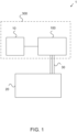
- the first arrangement 1 may also comprise a reference clock generator 10.
- the reference clock generator 10 and the control arrangement 100 may be coupled together releasably or non-releasably, for example on the same support.
- the first arrangement 1 may be a generator arrangement 300 comprising, at least, a reference clock generator 10 and control arrangement 100.
- the first arrangement 1 may comprise a coupling arrangement 30 for coupling the control arrangement 100 to the receiving system 20 for providing a plurality of phase-coherent oscillating signals for the receiving system 20.
- the coupling arrangement 30 may comprise a plurality of transmission lines for coupling the control arrangement 100 to the receiving system 20, for example by releasable coupling.
- the coupling arrangement 30 may further comprise one or more mixers (not illustrated), such as frequency mixers, for modulating the plurality of phase-coherent oscillating signals.
- the one or more mixers are located within a cryostat.
- the plurality of phase-coherent oscillating signals may comprise one or more carrier signals, which can thereby be mixed with a modulating signal, such as a control signal for a qubit for the receiving system 20.
- FIG. 2 illustrates a control arrangement 100 according to an example of the invention.
- the control arrangement 100 comprises a reference clock input arrangement 102 for providing a high-frequency reference clock signal.
- the high-frequency reference clock signal may be provided directly or indirectly from the reference clock generator 10. This signal can be provided from the reference clock generator 10 as disclosed above.
- the frequency of the high-frequency reference clock signal may be, for example 50-1000 MHz. In some embodiments, the frequency may be at least 100 MHz and/or at most 250 MHz, both of the upper and the lower limit having been found to provide improved functionality for the control arrangement 100, alone or in combination. Any frequency here may correspond to the nominal frequency of the reference clock generator 10.
- the reference clock input arrangement 102 may comprise a reference clock signal input 110 for inputting an initial reference clock signal. This allows indirectly providing the high-frequency reference clock signal from the reference clock generator 10.
- the reference clock generator 10 may be utilized for providing the initial reference clock signal.
- the reference clock input arrangement 102 may then comprise an initial phase-locked loop 120, which is coupled to the reference clock signal input 110 for providing a high-frequency reference clock signal, for example having a frequency of 100-250 MHz.
- the initial phase-locked loop may comprise an oscillator of the corresponding frequency.
- the frequency of the initial reference clock signal may be, for example 5-250 MHz. In some embodiments, the frequency may be 5-50 MHz. In particular, the frequency of 10 MHz has been found to provide additional benefits for scalable upconversion. The accuracy for the frequency can be 20 ppm (+/-) or better. Any frequency here may correspond to the nominal frequency of the reference clock generator 10.
- the initial reference clock signal may be a square-wave signal when inputted to the initial phase-locked loop 120.
- the reference clock input arrangement 102 may comprise a signal processing arrangement for adjusting the properties, such as shape, of the initial reference clock signal, for example situated between the reference clock signal input 110 and the initial phase-locked loop 120.
- the control arrangement 100 comprises a plurality of modules 130, where each module comprises a plurality of channels 160 for providing the plurality of phase-coherent oscillating signals.
- each module comprises a plurality of channels 160 for providing the plurality of phase-coherent oscillating signals.
- the number of modules 130 may be relatively small, for example 4-10, or larger, for example 10-100 or more.
- the number of channels 160 in each of the plurality of modules 130 may be relatively small, for example 4-10, but also larger, for example 10-100 or more.
- the reference clock input arrangement 102 may comprise a motherboard arrangement 104 for support and connectivity, for example for the initial phase-locked loop 120 and/or the first distribution arrangement 140.
- the motherboard arrangement 104 may comprise or be formed by one or more circuit boards arranged as a motherboard.
- the initial phase-locked loop 120 can be arranged on the motherboard arrangement 104.
- the reference clock signal input 110 may be arranged on the motherboard arrangement 104, for example providing a pluggable coupling for a transmission connection for the initial reference clock signal, such as a transmission line from the reference clock generator 10.
- each of the plurality of modules 130 may comprise at least one second circuit board 132 for providing support and connectivity for the respective module.
- each of the modules 130 may thereby be arranged at one or more module-specific circuit boards, which may be joined as one support. This allows efficient separation of the modules 130 from each other and from the motherboard arrangement 104. Any circuit boards mentioned herein may be printed circuit boards (PCB).
- PCB printed circuit boards
- the control arrangement 100 comprises a first distribution arrangement 140 for distributing the high-frequency reference clock signal in a phase-coherent manner to the plurality of modules.
- the first distribution arrangement 140 may comprise wiring for providing signal paths for the high-frequency reference clock signal to each of the modules 130, for example from the initial phase-locked loop 120. Two or more of the signal paths may be of equal length for maintaining the same phase for the respective modules 130. However, the signal paths may also be of different length since for phase-coherence it is not necessarily required that the phase is conserved as long as the phase-relation is deterministic.
- the first distribution arrangement 140 may comprise pluggable coupling for the plurality of modules 130.
- the first distribution arrangement 140 may comprise a plurality of plug/socket connections 142 for the plurality of modules 130, wherein each plug/socket connection comprises a first end and a second end, which are compatible with each other for insertion.
- a first end 134 of a plug/socket connection for example a plug, may be arranged at each of the plurality of modules 130.
- a second end of a plug/socket connection for example a socket, may be arranged at the reference clock input arrangement 102, for example on the motherboard arrangement 104 thereof.
- the plug/socket connection may comprise an edge connector, for example a PCI Express connector.
- the high-frequency reference clock signal may be a square-wave signal when provided for the modules 130.
- the control arrangement 100 may comprise a signal processing arrangement for adjusting the properties, such as shape, of the high-frequency clock signal. It may be arranged at the reference clock input arrangement 102, for example on the motherboard arrangement 104. It may also be situated at or before the first distribution arrangement 140.
- the plurality of shields 190 may comprise a plurality of separate screening boxes for rf shielding of respective channels 160.
- each of the plurality of channels 160 is separately covered for rf shielding by a shield 190 comprising sheet metal.
Landscapes
- Engineering & Computer Science (AREA)
- Theoretical Computer Science (AREA)
- Physics & Mathematics (AREA)
- General Physics & Mathematics (AREA)
- General Engineering & Computer Science (AREA)
- Nonlinear Science (AREA)
- Evolutionary Computation (AREA)
- Mathematical Physics (AREA)
- Condensed Matter Physics & Semiconductors (AREA)
- Data Mining & Analysis (AREA)
- Artificial Intelligence (AREA)
- Mathematical Analysis (AREA)
- Mathematical Optimization (AREA)
- Pure & Applied Mathematics (AREA)
- Computing Systems (AREA)
- Computational Mathematics (AREA)
- Software Systems (AREA)
- Stabilization Of Oscillater, Synchronisation, Frequency Synthesizers (AREA)
- Combinations Of Printed Boards (AREA)
- Variable-Direction Aerials And Aerial Arrays (AREA)
- Vehicle Body Suspensions (AREA)
- Container Filling Or Packaging Operations (AREA)
- Paper (AREA)
Claims (16)
- Agencement de commande (100) pour fournir une pluralité de signaux oscillants cohérents en phase à un agencement d'informatique quantique, l'agencement de commande (100) comprenant un agencement d'entrée d'horloge de référence pour fournir un signal d'horloge de référence haute fréquence, caractérisé par :- une pluralité de modules (130) comprenant chacun une pluralité de canaux (160) pour fournir la pluralité de signaux oscillants cohérents en phase,- un premier agencement de distribution (140) pour distribuer le signal d'horloge de référence haute fréquence de manière cohérente en phase à la pluralité de modules (130),- au sein de chacun de la pluralité de modules (130), un second agencement de distribution (150) pour distribuer en outre le signal d'horloge de référence haute fréquence distribué à ce module par ledit premier agencement de distribution (140) de manière cohérente en phase à la pluralité de canaux (160) du module (130) respectif, et- au sein de chacun de la pluralité de canaux (160), une première boucle verrouillée en phase (162) configurée pour la conversion-élévation du signal d'horloge de référence haute fréquence distribué à ce canal par le second agencement de distribution (150) du module respectif pour fournir l'un de la pluralité de signaux oscillants cohérents en phase.
- Agencement de commande (100) selon la revendication 1, dans lequel l'agencement d'entrée d'horloge de référence comprend :- une entrée (110) de signal d'horloge de référence pour fournir un signal d'horloge de référence initial ; et- une boucle verrouillée en phase initiale (120) couplée à l'entrée (110) de signal d'horloge de référence et configurée pour la conversion-élévation du signal d'horloge de référence initial pour fournir le signal d'horloge de référence haute fréquence.
- Agencement de commande (100) selon la revendication 1 ou la revendication 2, dans lequel l'agencement d'entrée d'horloge de référence comprend un agencement de carte mère (104) et dans lequel chacun de la pluralité de modules (130) comprend une carte (132) de circuit imprimé respective.
- Agencement de commande (100) selon l'une quelconque des revendications précédentes, dans lequel l'agencement d'entrée d'horloge de référence comprend un agencement de carte mère (104) et dans lequel chacun de la pluralité de modules (150) est agencé pour un couplage enfichable à l'agencement de carte mère (104).
- Agencement de commande (100) selon l'une quelconque des revendications précédentes, dans lequel chacun de la pluralité de modules (130) comprend une pluralité de blindages (190) pour le blindage contre les radiofréquences (rf) de chacun de la pluralité de canaux (160) du module (130) respectif.
- Agencement de commande (100) selon l'une quelconque des revendications précédentes, lorsqu'elles dépendent de la revendication 2, dans lequel le signal d'horloge de référence initial présente une fréquence de 5 à 50 MHz.
- Agencement de commande (100) selon l'une quelconque des revendications précédentes, dans lequel le signal d'horloge de référence haute fréquence présente une fréquence de 100 à 250 MHz et/ou chacun de la pluralité de signaux oscillants cohérents en phase présente une fréquence de 1 à 15 GHz.
- Agencement de commande (100) selon l'une quelconque des revendications précédentes, dans lequel l'amplitude et/ou la fréquence d'au moins un parmi la pluralité de signaux oscillants cohérents en phase sont réglables par un signal de commande numérique pour le canal respectif.
- Agencement de commande (100) selon l'une quelconque des revendications précédentes, comprenant une connexion de commande pour le réglage à distance de la fréquence et/ou de l'amplitude de la pluralité de signaux oscillants cohérents en phase.
- Agencement de générateur (300) pour fournir une pluralité de signaux oscillants cohérents en phase, l'agencement de générateur (300) comprenant l'agencement de commande (100) selon l'une quelconque des revendications 1 à 9 précédentes et un générateur d'horloge de référence (10) agencé pour fournir un signal d'horloge de référence pour fournir le signal d'horloge de référence haute fréquence.
- Agencement d'informatique quantique comprenant un agencement de commande (100) selon l'une quelconque des revendications 1 à 9 et un système (20) d'informatique quantique, dans lequel l'agencement de commande (100) est couplé au système (20) d'informatique quantique pour fournir ladite pluralité de signaux oscillants cohérents en phase au système (20) d'informatique quantique.
- Procédé (200) de fourniture d'une pluralité de signaux oscillants cohérents en phase à un agencement d'informatique quantique, le procédé comprenant la réception (230) d'un signal d'horloge de référence haute fréquence, caractérisé en ce que le procédé comprend :- la distribution (230) du signal d'horloge de référence haute fréquence de manière cohérente en phase à une pluralité de modules par un premier agencement de distribution,- au sein de chacun de la pluralité de modules, la distribution en outre (240), par un second agencement de distribution et de manière cohérente en phase, du signal d'horloge de référence haute fréquence distribué à ce module vers une pluralité de canaux du module respectif, et- au sein de chacun de la pluralité de canaux, la conversion-élévation (250), par une première boucle verrouillée en phase, du signal d'horloge de référence haute fréquence distribué à ce canal au sein du module respectif pour fournir l'un de la pluralité de signaux oscillants cohérents en phase.
- Procédé selon la revendication 12, comprenant :- la réception (210) d'un signal d'horloge de référence initial, et- la conversion-élévation (220) du signal d'horloge de référence initial pour fournir le signal d'horloge de référence haute fréquence.
- Procédé selon la revendication 13, dans lequel le signal d'horloge de référence initial présente une fréquence de 5 à 50 MHz.
- Procédé selon l'une quelconque des revendications 12 à 14, dans lequel le signal d'horloge de référence haute fréquence présente une fréquence de 100 à 250 MHz et/ou chacun de la pluralité de signaux oscillants cohérents en phase présente une fréquence de 1 à 15 GHz.
- Procédé selon l'une quelconque des revendications 13 à 15, comprenant le réglage de l'amplitude et/ou de la fréquence d'au moins un parmi la pluralité de signaux oscillants cohérents en phase par un signal de commande numérique pour le canal respectif.
Priority Applications (13)
| Application Number | Priority Date | Filing Date | Title |
|---|---|---|---|
| EP20156207.1A EP3863178B1 (fr) | 2020-02-07 | 2020-02-07 | Agencement et procédé de commande |
| EP25186663.8A EP4618420A3 (fr) | 2020-02-07 | 2020-02-07 | Agencement et procédé de commande |
| PL20156207.1T PL3863178T3 (pl) | 2020-02-07 | 2020-02-07 | Układ i sposób sterowania |
| TW110104002A TW202203585A (zh) | 2020-02-07 | 2021-02-03 | 控制設置及方法 |
| AU2021215359A AU2021215359B2 (en) | 2020-02-07 | 2021-02-04 | Control arrangement and method |
| US17/797,539 US12088309B2 (en) | 2020-02-07 | 2021-02-04 | Control arrangement and method |
| IL295314A IL295314B2 (en) | 2020-02-07 | 2021-02-04 | Control arrangement and method |
| PCT/FI2021/050077 WO2021156545A1 (fr) | 2020-02-07 | 2021-02-04 | Dispositif et procédé de commande |
| JP2022547286A JP7659567B2 (ja) | 2020-02-07 | 2021-02-04 | 制御装置及び方法 |
| KR1020227031139A KR102898984B1 (ko) | 2020-02-07 | 2021-02-04 | 제어 장치 및 방법 |
| CA3170001A CA3170001A1 (fr) | 2020-02-07 | 2021-02-04 | Dispositif et procede de commande |
| CN202180013424.XA CN115176419A (zh) | 2020-02-07 | 2021-02-04 | 控制装置和方法 |
| US18/797,011 US20240396560A1 (en) | 2020-02-07 | 2024-08-07 | Control arrangement and method |
Applications Claiming Priority (1)
| Application Number | Priority Date | Filing Date | Title |
|---|---|---|---|
| EP20156207.1A EP3863178B1 (fr) | 2020-02-07 | 2020-02-07 | Agencement et procédé de commande |
Related Child Applications (1)
| Application Number | Title | Priority Date | Filing Date |
|---|---|---|---|
| EP25186663.8A Division EP4618420A3 (fr) | 2020-02-07 | 2020-02-07 | Agencement et procédé de commande |
Publications (3)
| Publication Number | Publication Date |
|---|---|
| EP3863178A1 EP3863178A1 (fr) | 2021-08-11 |
| EP3863178C0 EP3863178C0 (fr) | 2025-07-02 |
| EP3863178B1 true EP3863178B1 (fr) | 2025-07-02 |
Family
ID=69528625
Family Applications (2)
| Application Number | Title | Priority Date | Filing Date |
|---|---|---|---|
| EP20156207.1A Active EP3863178B1 (fr) | 2020-02-07 | 2020-02-07 | Agencement et procédé de commande |
| EP25186663.8A Pending EP4618420A3 (fr) | 2020-02-07 | 2020-02-07 | Agencement et procédé de commande |
Family Applications After (1)
| Application Number | Title | Priority Date | Filing Date |
|---|---|---|---|
| EP25186663.8A Pending EP4618420A3 (fr) | 2020-02-07 | 2020-02-07 | Agencement et procédé de commande |
Country Status (11)
| Country | Link |
|---|---|
| US (2) | US12088309B2 (fr) |
| EP (2) | EP3863178B1 (fr) |
| JP (1) | JP7659567B2 (fr) |
| KR (1) | KR102898984B1 (fr) |
| CN (1) | CN115176419A (fr) |
| AU (1) | AU2021215359B2 (fr) |
| CA (1) | CA3170001A1 (fr) |
| IL (1) | IL295314B2 (fr) |
| PL (1) | PL3863178T3 (fr) |
| TW (1) | TW202203585A (fr) |
| WO (1) | WO2021156545A1 (fr) |
Families Citing this family (1)
| Publication number | Priority date | Publication date | Assignee | Title |
|---|---|---|---|---|
| EP3886321A1 (fr) | 2020-03-24 | 2021-09-29 | IQM Finland Oy | Circuit intégré cryogénique, module intégré et agencement de production et de détection d'excitation et de lecture de signaux de bits quantiques |
Family Cites Families (13)
| Publication number | Priority date | Publication date | Assignee | Title |
|---|---|---|---|---|
| JP4056145B2 (ja) * | 1998-09-17 | 2008-03-05 | 株式会社ルネサステクノロジ | Pll回路およびそれを用いた無線通信端末機器 |
| JP2003308133A (ja) * | 2002-02-18 | 2003-10-31 | Matsushita Electric Ind Co Ltd | 多相クロック伝送回路及び多相クロック伝送方法 |
| US20080205550A1 (en) * | 2007-02-28 | 2008-08-28 | Ahmadreza Rofougaran | Method and System for Using a Phase Locked Loop for Upconversion in a Wideband Polar Transmitter |
| WO2014109964A1 (fr) * | 2013-01-08 | 2014-07-17 | Rambus Inc. | Circuit intégré comprenant un ensemble de circuits permettant de déterminer des paramètres pour un oscillateur verrouillé par injection |
| US10374788B2 (en) * | 2016-08-17 | 2019-08-06 | Qorvo Us, Inc. | Phase locked loop (PLL)-less millimeter wave power head |
| US10476509B2 (en) * | 2016-12-07 | 2019-11-12 | Integrated Device Technology, Inc. | Time slotted bus system for multiple coupled digital phase-locked loops |
| US10419005B2 (en) * | 2016-12-14 | 2019-09-17 | Taiwan Semiconductor Manufacturing Co., Ltd. | Phase-locked-loop architecture |
| CN118117305A (zh) * | 2016-12-21 | 2024-05-31 | 英特尔公司 | 无线通信技术、装置和方法 |
| US10705199B2 (en) * | 2017-11-30 | 2020-07-07 | Urban Canyon Flight | Aviation transponder |
| US10680623B2 (en) * | 2018-04-17 | 2020-06-09 | Huawei Technologies Co., Ltd. | System for coherent distribution of oscillator signal |
| CN112514245B (zh) * | 2018-06-11 | 2024-06-25 | 苏州斯威特科技有限公司 | 宽频带毫米波前端集成电路 |
| US11410068B2 (en) * | 2018-07-30 | 2022-08-09 | International Business Machines Corporation | Quantum processing system including a modulated RF generator with synchronized components |
| US10938465B1 (en) * | 2019-05-14 | 2021-03-02 | Space Exploration Technologies Corp. | Channel aggregation digital beamforming |
-
2020
- 2020-02-07 EP EP20156207.1A patent/EP3863178B1/fr active Active
- 2020-02-07 PL PL20156207.1T patent/PL3863178T3/pl unknown
- 2020-02-07 EP EP25186663.8A patent/EP4618420A3/fr active Pending
-
2021
- 2021-02-03 TW TW110104002A patent/TW202203585A/zh unknown
- 2021-02-04 AU AU2021215359A patent/AU2021215359B2/en active Active
- 2021-02-04 IL IL295314A patent/IL295314B2/en unknown
- 2021-02-04 US US17/797,539 patent/US12088309B2/en active Active
- 2021-02-04 KR KR1020227031139A patent/KR102898984B1/ko active Active
- 2021-02-04 WO PCT/FI2021/050077 patent/WO2021156545A1/fr not_active Ceased
- 2021-02-04 JP JP2022547286A patent/JP7659567B2/ja active Active
- 2021-02-04 CN CN202180013424.XA patent/CN115176419A/zh active Pending
- 2021-02-04 CA CA3170001A patent/CA3170001A1/fr active Pending
-
2024
- 2024-08-07 US US18/797,011 patent/US20240396560A1/en active Pending
Also Published As
| Publication number | Publication date |
|---|---|
| CN115176419A (zh) | 2022-10-11 |
| EP3863178C0 (fr) | 2025-07-02 |
| IL295314B2 (en) | 2025-12-01 |
| AU2021215359A1 (en) | 2022-09-29 |
| KR20220137972A (ko) | 2022-10-12 |
| EP4618420A3 (fr) | 2025-11-26 |
| EP4618420A2 (fr) | 2025-09-17 |
| IL295314A (en) | 2022-10-01 |
| KR102898984B1 (ko) | 2025-12-12 |
| US20240396560A1 (en) | 2024-11-28 |
| EP3863178A1 (fr) | 2021-08-11 |
| CA3170001A1 (fr) | 2021-08-12 |
| AU2021215359B2 (en) | 2026-03-12 |
| IL295314B1 (en) | 2025-08-01 |
| US12088309B2 (en) | 2024-09-10 |
| US20230049369A1 (en) | 2023-02-16 |
| JP2023513143A (ja) | 2023-03-30 |
| JP7659567B2 (ja) | 2025-04-09 |
| PL3863178T3 (pl) | 2026-03-02 |
| WO2021156545A1 (fr) | 2021-08-12 |
| TW202203585A (zh) | 2022-01-16 |
Similar Documents
| Publication | Publication Date | Title |
|---|---|---|
| US20150087248A1 (en) | Fully integrated millimeter-wave radio frequency system | |
| US20240396560A1 (en) | Control arrangement and method | |
| CN105187060A (zh) | 一种低相位噪声的锁相环电路及其实现方法 | |
| JP7303506B2 (ja) | 量子コンピュータの制御装置 | |
| US8902007B2 (en) | Clock distributor and electronic device | |
| HK40055260A (en) | Control arrangement and method | |
| US8692595B1 (en) | Transceiver circuitry with multiple phase-locked loops | |
| US8981854B2 (en) | Clock distributor and electronic apparatus | |
| US20160072436A1 (en) | Method and Apparatus of Synchronizing Oscillators | |
| CN215867554U (zh) | 一种任意波形发生器底板 | |
| US7114092B2 (en) | Method of supplying a required clock frequency by a clock generator module through interface communication with a mainboard | |
| CN108259038A (zh) | 一种宽带低杂散捷变频频率合成装置 | |
| Keitch et al. | Programmable and scalable radio-frequency pulse sequence generator for multi-qubit quantum information experiments | |
| Hulsart et al. | A versatile BPM signal processing system based on the XILINX ZYNQ SOC | |
| CN206865415U (zh) | 正弦波发生电路及测距装置 | |
| US7750748B2 (en) | Method and apparatus for distributing clock signal using standing waves | |
| CN222167497U (zh) | 一种灵活可配置的系统时钟处理系统 | |
| CN223488208U (zh) | 一种流式细胞仪中一个时钟扩展成多路同步时钟的电路 | |
| JP2014158114A (ja) | クロック発生デバイス | |
| CN113721056A (zh) | 一种可扩展的任意波形发生器底板 | |
| CN110808758A (zh) | 一种小型化pxi总线扩频装置及扩频方法 | |
| Dayaratna et al. | On orbit programmable frequency generation system for JCSAT 9 spacecraft |
Legal Events
| Date | Code | Title | Description |
|---|---|---|---|
| PUAI | Public reference made under article 153(3) epc to a published international application that has entered the european phase |
Free format text: ORIGINAL CODE: 0009012 |
|
| STAA | Information on the status of an ep patent application or granted ep patent |
Free format text: STATUS: THE APPLICATION HAS BEEN PUBLISHED |
|
| AK | Designated contracting states |
Kind code of ref document: A1 Designated state(s): AL AT BE BG CH CY CZ DE DK EE ES FI FR GB GR HR HU IE IS IT LI LT LU LV MC MK MT NL NO PL PT RO RS SE SI SK SM TR |
|
| STAA | Information on the status of an ep patent application or granted ep patent |
Free format text: STATUS: REQUEST FOR EXAMINATION WAS MADE |
|
| 17P | Request for examination filed |
Effective date: 20220131 |
|
| RBV | Designated contracting states (corrected) |
Designated state(s): AL AT BE BG CH CY CZ DE DK EE ES FI FR GB GR HR HU IE IS IT LI LT LU LV MC MK MT NL NO PL PT RO RS SE SI SK SM TR |
|
| REG | Reference to a national code |
Ref country code: HK Ref legal event code: DE Ref document number: 40055260 Country of ref document: HK |
|
| STAA | Information on the status of an ep patent application or granted ep patent |
Free format text: STATUS: EXAMINATION IS IN PROGRESS |
|
| 17Q | First examination report despatched |
Effective date: 20230814 |
|
| GRAP | Despatch of communication of intention to grant a patent |
Free format text: ORIGINAL CODE: EPIDOSNIGR1 |
|
| STAA | Information on the status of an ep patent application or granted ep patent |
Free format text: STATUS: GRANT OF PATENT IS INTENDED |
|
| INTG | Intention to grant announced |
Effective date: 20240917 |
|
| GRAJ | Information related to disapproval of communication of intention to grant by the applicant or resumption of examination proceedings by the epo deleted |
Free format text: ORIGINAL CODE: EPIDOSDIGR1 |
|
| STAA | Information on the status of an ep patent application or granted ep patent |
Free format text: STATUS: EXAMINATION IS IN PROGRESS |
|
| INTC | Intention to grant announced (deleted) | ||
| GRAP | Despatch of communication of intention to grant a patent |
Free format text: ORIGINAL CODE: EPIDOSNIGR1 |
|
| STAA | Information on the status of an ep patent application or granted ep patent |
Free format text: STATUS: GRANT OF PATENT IS INTENDED |
|
| INTG | Intention to grant announced |
Effective date: 20250130 |
|
| GRAS | Grant fee paid |
Free format text: ORIGINAL CODE: EPIDOSNIGR3 |
|
| GRAA | (expected) grant |
Free format text: ORIGINAL CODE: 0009210 |
|
| STAA | Information on the status of an ep patent application or granted ep patent |
Free format text: STATUS: THE PATENT HAS BEEN GRANTED |
|
| AK | Designated contracting states |
Kind code of ref document: B1 Designated state(s): AL AT BE BG CH CY CZ DE DK EE ES FI FR GB GR HR HU IE IS IT LI LT LU LV MC MK MT NL NO PL PT RO RS SE SI SK SM TR |
|
| REG | Reference to a national code |
Ref country code: GB Ref legal event code: FG4D |
|
| REG | Reference to a national code |
Ref country code: CH Ref legal event code: EP |
|
| REG | Reference to a national code |
Ref country code: DE Ref legal event code: R096 Ref document number: 602020053625 Country of ref document: DE |
|
| REG | Reference to a national code |
Ref country code: IE Ref legal event code: FG4D |
|
| U01 | Request for unitary effect filed |
Effective date: 20250731 |
|
| U07 | Unitary effect registered |
Designated state(s): AT BE BG DE DK EE FI FR IT LT LU LV MT NL PT RO SE SI Effective date: 20250811 |
|
| PG25 | Lapsed in a contracting state [announced via postgrant information from national office to epo] |
Ref country code: IS Free format text: LAPSE BECAUSE OF FAILURE TO SUBMIT A TRANSLATION OF THE DESCRIPTION OR TO PAY THE FEE WITHIN THE PRESCRIBED TIME-LIMIT Effective date: 20251102 |
|
| PG25 | Lapsed in a contracting state [announced via postgrant information from national office to epo] |
Ref country code: NO Free format text: LAPSE BECAUSE OF FAILURE TO SUBMIT A TRANSLATION OF THE DESCRIPTION OR TO PAY THE FEE WITHIN THE PRESCRIBED TIME-LIMIT Effective date: 20251002 |
|
| PG25 | Lapsed in a contracting state [announced via postgrant information from national office to epo] |
Ref country code: HR Free format text: LAPSE BECAUSE OF FAILURE TO SUBMIT A TRANSLATION OF THE DESCRIPTION OR TO PAY THE FEE WITHIN THE PRESCRIBED TIME-LIMIT Effective date: 20250702 |
|
| PG25 | Lapsed in a contracting state [announced via postgrant information from national office to epo] |
Ref country code: GR Free format text: LAPSE BECAUSE OF FAILURE TO SUBMIT A TRANSLATION OF THE DESCRIPTION OR TO PAY THE FEE WITHIN THE PRESCRIBED TIME-LIMIT Effective date: 20251003 |
|
| PG25 | Lapsed in a contracting state [announced via postgrant information from national office to epo] |
Ref country code: CZ Free format text: LAPSE BECAUSE OF FAILURE TO SUBMIT A TRANSLATION OF THE DESCRIPTION OR TO PAY THE FEE WITHIN THE PRESCRIBED TIME-LIMIT Effective date: 20250702 |
|
| PG25 | Lapsed in a contracting state [announced via postgrant information from national office to epo] |
Ref country code: RS Free format text: LAPSE BECAUSE OF FAILURE TO SUBMIT A TRANSLATION OF THE DESCRIPTION OR TO PAY THE FEE WITHIN THE PRESCRIBED TIME-LIMIT Effective date: 20251002 |
|
| PG25 | Lapsed in a contracting state [announced via postgrant information from national office to epo] |
Ref country code: ES Free format text: LAPSE BECAUSE OF FAILURE TO SUBMIT A TRANSLATION OF THE DESCRIPTION OR TO PAY THE FEE WITHIN THE PRESCRIBED TIME-LIMIT Effective date: 20250702 |
|
| U20 | Renewal fee for the european patent with unitary effect paid |
Year of fee payment: 7 Effective date: 20260225 |
|
| PG25 | Lapsed in a contracting state [announced via postgrant information from national office to epo] |
Ref country code: SM Free format text: LAPSE BECAUSE OF FAILURE TO SUBMIT A TRANSLATION OF THE DESCRIPTION OR TO PAY THE FEE WITHIN THE PRESCRIBED TIME-LIMIT Effective date: 20250702 |
|
| PGFP | Annual fee paid to national office [announced via postgrant information from national office to epo] |
Ref country code: GB Payment date: 20260220 Year of fee payment: 7 |
|
| PGFP | Annual fee paid to national office [announced via postgrant information from national office to epo] |
Ref country code: PL Payment date: 20260203 Year of fee payment: 7 |
|
| PG25 | Lapsed in a contracting state [announced via postgrant information from national office to epo] |
Ref country code: SK Free format text: LAPSE BECAUSE OF FAILURE TO SUBMIT A TRANSLATION OF THE DESCRIPTION OR TO PAY THE FEE WITHIN THE PRESCRIBED TIME-LIMIT Effective date: 20250702 |