EP3864498B1 - Alimentation par boutons - Google Patents
Alimentation par boutons Download PDFInfo
- Publication number
- EP3864498B1 EP3864498B1 EP19787056.1A EP19787056A EP3864498B1 EP 3864498 B1 EP3864498 B1 EP 3864498B1 EP 19787056 A EP19787056 A EP 19787056A EP 3864498 B1 EP3864498 B1 EP 3864498B1
- Authority
- EP
- European Patent Office
- Prior art keywords
- wire
- touch panel
- hole
- user input
- button
- Prior art date
- Legal status (The legal status is an assumption and is not a legal conclusion. Google has not performed a legal analysis and makes no representation as to the accuracy of the status listed.)
- Active
Links
Images


Classifications
-
- G—PHYSICS
- G06—COMPUTING OR CALCULATING; COUNTING
- G06F—ELECTRIC DIGITAL DATA PROCESSING
- G06F3/00—Input arrangements for transferring data to be processed into a form capable of being handled by the computer; Output arrangements for transferring data from processing unit to output unit, e.g. interface arrangements
- G06F3/01—Input arrangements or combined input and output arrangements for interaction between user and computer
- G06F3/02—Input arrangements using manually operated switches, e.g. using keyboards or dials
- G06F3/0202—Constructional details or processes of manufacture of the input device
-
- A—HUMAN NECESSITIES
- A63—SPORTS; GAMES; AMUSEMENTS
- A63F—CARD, BOARD, OR ROULETTE GAMES; INDOOR GAMES USING SMALL MOVING PLAYING BODIES; VIDEO GAMES; GAMES NOT OTHERWISE PROVIDED FOR
- A63F13/00—Video games, i.e. games using an electronically generated display having two or more dimensions
- A63F13/20—Input arrangements for video game devices
- A63F13/21—Input arrangements for video game devices characterised by their sensors, purposes or types
- A63F13/214—Input arrangements for video game devices characterised by their sensors, purposes or types for locating contacts on a surface, e.g. floor mats or touch pads
-
- G—PHYSICS
- G06—COMPUTING OR CALCULATING; COUNTING
- G06F—ELECTRIC DIGITAL DATA PROCESSING
- G06F3/00—Input arrangements for transferring data to be processed into a form capable of being handled by the computer; Output arrangements for transferring data from processing unit to output unit, e.g. interface arrangements
- G06F3/01—Input arrangements or combined input and output arrangements for interaction between user and computer
- G06F3/03—Arrangements for converting the position or the displacement of a member into a coded form
- G06F3/033—Pointing devices displaced or positioned by the user, e.g. mice, trackballs, pens or joysticks; Accessories therefor
- G06F3/0338—Pointing devices displaced or positioned by the user, e.g. mice, trackballs, pens or joysticks; Accessories therefor with detection of limited linear or angular displacement of an operating part of the device from a neutral position, e.g. isotonic or isometric joysticks
-
- G—PHYSICS
- G06—COMPUTING OR CALCULATING; COUNTING
- G06F—ELECTRIC DIGITAL DATA PROCESSING
- G06F3/00—Input arrangements for transferring data to be processed into a form capable of being handled by the computer; Output arrangements for transferring data from processing unit to output unit, e.g. interface arrangements
- G06F3/01—Input arrangements or combined input and output arrangements for interaction between user and computer
- G06F3/03—Arrangements for converting the position or the displacement of a member into a coded form
- G06F3/033—Pointing devices displaced or positioned by the user, e.g. mice, trackballs, pens or joysticks; Accessories therefor
- G06F3/0362—Pointing devices displaced or positioned by the user, e.g. mice, trackballs, pens or joysticks; Accessories therefor with detection of one-dimensional [1D] translations or rotations of an operating part of the device, e.g. scroll wheels, sliders, knobs, rollers or belts
-
- G—PHYSICS
- G06—COMPUTING OR CALCULATING; COUNTING
- G06F—ELECTRIC DIGITAL DATA PROCESSING
- G06F3/00—Input arrangements for transferring data to be processed into a form capable of being handled by the computer; Output arrangements for transferring data from processing unit to output unit, e.g. interface arrangements
- G06F3/01—Input arrangements or combined input and output arrangements for interaction between user and computer
- G06F3/03—Arrangements for converting the position or the displacement of a member into a coded form
- G06F3/041—Digitisers, e.g. for touch screens or touch pads, characterised by the transducing means
- G06F3/0416—Control or interface arrangements specially adapted for digitisers
- G06F3/04164—Connections between sensors and controllers, e.g. routing lines between electrodes and connection pads
-
- G—PHYSICS
- G06—COMPUTING OR CALCULATING; COUNTING
- G06F—ELECTRIC DIGITAL DATA PROCESSING
- G06F3/00—Input arrangements for transferring data to be processed into a form capable of being handled by the computer; Output arrangements for transferring data from processing unit to output unit, e.g. interface arrangements
- G06F3/01—Input arrangements or combined input and output arrangements for interaction between user and computer
- G06F3/03—Arrangements for converting the position or the displacement of a member into a coded form
- G06F3/041—Digitisers, e.g. for touch screens or touch pads, characterised by the transducing means
- G06F3/044—Digitisers, e.g. for touch screens or touch pads, characterised by the transducing means by capacitive means
- G06F3/0446—Digitisers, e.g. for touch screens or touch pads, characterised by the transducing means by capacitive means using a grid-like structure of electrodes in at least two directions, e.g. using row and column electrodes
-
- G—PHYSICS
- G06—COMPUTING OR CALCULATING; COUNTING
- G06F—ELECTRIC DIGITAL DATA PROCESSING
- G06F2203/00—Indexing scheme relating to G06F3/00 - G06F3/048
- G06F2203/041—Indexing scheme relating to G06F3/041 - G06F3/045
- G06F2203/04103—Manufacturing, i.e. details related to manufacturing processes specially suited for touch sensitive devices
-
- G—PHYSICS
- G06—COMPUTING OR CALCULATING; COUNTING
- G06F—ELECTRIC DIGITAL DATA PROCESSING
- G06F2203/00—Indexing scheme relating to G06F3/00 - G06F3/048
- G06F2203/041—Indexing scheme relating to G06F3/041 - G06F3/045
- G06F2203/04112—Electrode mesh in capacitive digitiser: electrode for touch sensing is formed of a mesh of very fine, normally metallic, interconnected lines that are almost invisible to see. This provides a quite large but transparent electrode surface, without need for ITO or similar transparent conductive material
-
- H—ELECTRICITY
- H01—ELECTRIC ELEMENTS
- H01H—ELECTRIC SWITCHES; RELAYS; SELECTORS; EMERGENCY PROTECTIVE DEVICES
- H01H13/00—Switches having rectilinearly-movable operating part or parts adapted for pushing or pulling in one direction only, e.g. push-button switch
- H01H13/02—Details
- H01H13/12—Movable parts; Contacts mounted thereon
- H01H13/14—Operating parts, e.g. push-button
-
- H—ELECTRICITY
- H01—ELECTRIC ELEMENTS
- H01H—ELECTRIC SWITCHES; RELAYS; SELECTORS; EMERGENCY PROTECTIVE DEVICES
- H01H2231/00—Applications
- H01H2231/008—Video game
-
- H—ELECTRICITY
- H01—ELECTRIC ELEMENTS
- H01H—ELECTRIC SWITCHES; RELAYS; SELECTORS; EMERGENCY PROTECTIVE DEVICES
- H01H2239/00—Miscellaneous
- H01H2239/006—Containing a capacitive switch or usable as such
-
- H—ELECTRICITY
- H01—ELECTRIC ELEMENTS
- H01H—ELECTRIC SWITCHES; RELAYS; SELECTORS; EMERGENCY PROTECTIVE DEVICES
- H01H2300/00—Orthogonal indexing scheme relating to electric switches, relays, selectors or emergency protective devices covered by H01H
- H01H2300/024—Avoid unwanted operation
Definitions
- input devices which human operators can interact with to thereby provide an input indicating a selection.
- conventional input devices include mechanical input devices like mechanical buttons or keys or joystick or track balls or sliders.
- Other types of input devices like touchscreens or NFC readers are also known.
- Touchscreens in particular are increasingly popular and these allow a user to make selections and indicate choice by touching a surface of a touch panel in one or multiple locations with those locations being associated with regions displayed on an underlying display screen. By correlating detected touch positions in the plane of the touch panel with corresponding display positions in the plane of the underlying display a user can select one or more choices. Such selection can be used to indicate an instruction or for many other purposes.
- a touch panel is a clear panel with a touch sensitive surface.
- the touch panel is positioned in front of a display so that the touch sensitive surface covers the viewable area of the display screen.
- the touch panel and associated screen together can be referred to as a touchscreen or display arrangement.
- the track widths on such FPC using a printed ink is around the 60 ⁇ m to 80 ⁇ m feature size which is in fact very visible when placed directly in front of an LCD. Such feature sizes are certainly visible to the human eye and can cause Moiré fringing effects when placed in front of a powered LCD.
- Another issue with printed conductive tracks on a transparent PET film is that the depth of conductive track feature size is very thin ⁇ 1 ⁇ m, and this coupled with the fact that most conductive inks have a high resistance compare to traditional copper tracks/wire, makes the printed tracks not desirable in terms of having high resistance which means that the tracks cannot be very long, are not power efficient and difficult to drive with electronics.
- a method of manufacturing a touch panel for a touchscreen comprising the steps of:
- the method further comprises securing a flexible connector strip that comprises a plurality of first conductive pads to the electrical connectors whereby each pad is in respective electrical connection with at least one electrical connector.
- the method further comprises securing a plurality of further conduction pads of the connector strip, each connected to a respective one of the first conduction pads, to respective electrical contacts of the user input device.
- the method further comprises plotting the wire in a pattern whereby at each intersection, wire that provides touch electrodes crosses wire that provides an electrical connector substantially orthogonally.
- the method further comprises providing the transparent substrate by providing a glass substrate comprising at least one pre-cut through hole.
- the method further comprises the step of providing touch electrodes comprises cutting previously plotted wire in a plurality of locations to thereby provide a plurality of X and Y touch electrodes.
- the step of providing electrical connectors comprises cutting previously plotted wire in a plurality of locations to thereby provide a plurality of distinct lengths of wire that extend from an edge region of the substrate to a location over the transparent support within an imaginary boundary associated with an edge of a through hole in the substrate.
- the method further comprises providing a user input device at the through hole by securing a mechanical button or joystick or the like to the substrate at the through hole whereby at least one contact switch of the user input device is electrically connected with at least one electrical connector provided via the further portion of the plotted wire.
- the touch electrodes comprise a first group of electrodes that extend across a region of the substrate following a constant repetitive pathway and a further group of electrodes that extend across the substrate following the same constant repetitive pathway for a portion of their length but that include, proximate to a through hole, a modified pathway around an edge of a through hole.
- each electrical connector comprises at least one end portion of one or more sections of plotted wire that are electrically connected to a pad of a flexible connector strip.
- the touch panel further comprises a user input device at each through hole in the substrate, each user input device comprising a fascia member at a touch surface of the substrate, a base member spaced apart from but secured to the fascia member, a user movement member between the fascia member and the base member when the user movement member is moveable by a touch panel users hand; and at least one switch element, that has a state selectable by movement of user movement member, that is in electrical communication, via at least one electrical connector, to a controller of the touch panel.
- a touch panel of a touchscreen recognises an actual touch or touches as a touch event or multiple touch events on a surface of the touch panel and thereafter outputs signals representative of this information to a host device.
- the host device can be a computer such as a desktop, hand held or tablet computer or laptop. The host device performs an action based on the touch event.
- Figure 1 illustrates a table top arcade game machine 100.
- the arcade game machine 100 is an example of a device with which certain embodiments of the present invention can be utilised.
- Other such machines include information kiosks, ATMs, industrial machines or displays or gaming machines or the like.
- buttons 160 located at the centre of each of the four edges of the generally rectangular touchscreen. It will be appreciated that certain embodiments of the present are not limited in terms of the shape and size of touchscreen utilised nor the location of any mechanical user input device such as the buttons within that touchscreen. For example, buttons may be aligned along a common edge or, as shown in Figure 1 , at different edges or indeed alternatively or additionally in corner regions or in a central region of a touchscreen.
- the arcade game machine 100 shown in Figure 1 also has four user rests 170 which extend outwards as ears from the upper surface and on which a user can rest their elbows or arms or a beverage.
- the arcade game machine shown in Figure 1 has an illuminated region under the touchscreen which enhances the aesthetic appeal of the machine. It will be understood that whilst the arcade game machine 100 shown in Figure 1 has a display area which extends substantially across the whole of the upper surface of the machine certain other embodiments of the present invention could be formed with a touchscreen which forms only a portion of an upper surface enabling remaining regions of the upper surface to be used for other purposes and/or to display other imagery. Likewise, the touchscreen could be vertical or angled with respect to the floor.
- a transparent film layer 240 is provided on the lower (in Figure 2 ) surface of the adhesive layer 235.
- Part of this film layer 240 includes a though hole having an edge which is coincident with (and thus registration with) the edge 245 of the through hole 225 in the substrate.
- a tail like extension 250 of the film layer 240 extends beyond the edge 245 of the glass substrate and this provides a transparent support.
- the transparent support extends over at least a region of the through hole.
- the lower (in the orientation shown in Figure 2 ) surface of the film layer 240 is provided with an adhesive layer 260 which includes plotted wires thereupon.
- the plotted wires provide touch electrodes for a touch panel of the touchscreen and also are utilised to help provide a plurality of electrical connectors for the button (or other such user input device) secured at the through hole 225.
- a further film layer 270 covers the electrodes and adhesive.
- a first flexible cable 270 is provided at an edge to connect with the electrodes leading to a controller.
- a further flexible cable 280 connects to the electrical connectors provided by plotted wired which are interleaved with the plotted wires that form the touch electrodes and this further flexible cable 280 is connected to the micro switch or other switching element of the user input device that requires power supply and/or data transmission connection.
- a grid of electrodes is thus provided on a lower surface of the substrate.
- the grid of electrodes is a grid of fine wires generated on an adhesive layer using a plotting technique.
- the wires have a diameter region of 4 to 40 microns. Aptly the wire diameter is 5 to 18 microns. Aptly the wires are coated with a thin electrically insulating material. It will be appreciated that in examples not covered by the claims the electrode grid could be created using other electrode forming techniques such as by deposition of an ITO layer or the like.
- the touchscreen thus includes a relatively short effectively transparent flexible cable which connects the button output to a button controller. Unlike other prior art solutions this is far less visible to the naked human eye than has previously been possible.
- the button controller can be connected to the computer system host arcade game machine.
- a display (not shown) lies underneath the touch panel. In this way information displayed from the upper surface of the display can be seen by a human user through the touch panel located above the display. A user observing the displayed imagery or other such visual cues touches relative points on the upper surface of the touch panel and/or presses a button within the active area of the touch panel to thereby provide user input which effectively makes respective user selections.
- Figure 3 helps illustrate the grid 300 of electrodes arranged in a predetermined pattern for the touchscreen.
- the touch panel illustrated is a capacitive sensing touch panel and this includes touch electrodes which include drive electrodes and sensor electrodes accordingly which are driven and read via respective connectors 310.
- touch electrodes which include drive electrodes and sensor electrodes accordingly which are driven and read via respective connectors 310.
- all electrodes can be connected from a single side of the electrode grid meaning that a very thin surround only is required for the touch panel. It will be appreciated that other connectivity strategies could be utilised.
- Figure 3 helps illustrate how in addition to the wire sections that form the touch electrodes for the touchscreen other sections of wire are provided in a similar way which extend across the active area of the touchscreen and then around the edge of the active area to respective connectors.
- These wires are used to provide power and/or data communication with the mechanical user input devices located at the through holes of the touchscreen.
- wire which is provided in the same way that wire for the touch electrodes is provided can be made use of for providing power and/or data input/output.
- Making use of such fine wires which are effectively invisible to the naked eye for a substantial amount of the connection vastly reduces the visibility of such connecting elements relative to prior art techniques.
- the sections reduce the visibility of such connecting elements relative to prior art techniques.
- the sections of wire for the touch electrodes and/or the connectors may be provided by plotting a single wire in a long path and then subsequently cutting the wire in numerous locations to form separate sections.
- the touch electrodes have a pathway which does not pass through the area where the buttons 190, 195 are located.
- a first excluded zone 310 is associated with a through hole in the substrate 230 where the respective button 160 is located and a further excluded zone 320 is associated with another through hole through the substrate 220 where a further button 160 is located.
- the pathway of the electrodes is different close to and immediately surrounding each excluded zone relative to the pathway which is otherwise followed by electrodes in regions of the active area of the touch panel where the buttons are not located.
- An inner region of the electrode array defines an active area 330 of the touch panel.
- Figure 4 helps illustrate the pathway of electrodes surrounding a round hole in a touchscreen.
- the touch electrodes and electrical connection electrodes are shown terminating in an adjacent edge region for the sake of clarity. It will be understood that the skilled person will understand that once the plotted electrodes reach an edge region they may be fed directly off that edge region (in a manner similar to that shown in Figure 4 ) or around an edge to a common edge region (in a manner more like that shown in Figure 3 ).
- Figure 4 illustrates the edge 245 of a through hole 225 in more detail.
- a margin 410 is (for a round hole) a ring-like region which contains no touch electrodes and which immediately surrounds the edge of the hole. Aptly the margin is 1 to 3 mm wide.
- the drive electrodes and sensor electrodes which form part of the touch electrodes run approximately up and down vertically and left to right horizontally (in the orientation shown in Figure 4 ). It will be appreciated that other orientations could be utilised according to certain other embodiments of the present invention. Whilst the touch electrodes do not encroach within the margin, wire associated with electrical connectors for the user input device does cross the margin where the wire extends over the surface of the tail- like extension 250 of the film layer 240 that provides the transparent support.
- Figure 4 illustrates a pathway 420 for one particular wire that helps provide an electrical connection for the button in more detail.
- the pathway 420 which is shown highlighted (and thus broader than the other wires) in Figure 4 is provided by a section of wire 430.
- the wire 430 has a first end region 435 at an edge of the touchscreen. At the first end region 435 the wire has a sinusoidal or other labyrinthine-like shape. This introduces an overlength of wire which helps overcome stress problems.
- a respective contact pad carried by a flexi tail connector 270 overlies and is secured in electrical contact with the wire. Since the wire 430 is plotted as an insulated wire the insulation should first be removed from the end region 435 of the wire prior to electrical connection with the contact pad of the flexi tail connector.
- the wire 430 is electrically connected to the flexi tail in this way and from the flexi tail a connection can be made to the onboard controller of the host machine.
- the wire 430 then takes a pathway in a linear fashion away from the flexi tail at the edge towards the through hole in the button.
- the pathway 420 then turns around 90° to the left (in the orientation shown in Figure 4 ), continues forward for a portion and then turns right by around 90° leading towards the area where touch electrodes are provided.
- the pathway then extends from the region where the touch electrodes begin towards the margin surrounding a through hole.
- the pathway 420 turns so that adjacent wires pass in a substantially orthogonal manner. This helps reduce undesired coupling or interference effects.
- the wire 430 turns and passes over (or under) the touch electrodes which have a pathway that circumvents the through hole. From there the wire 430 turns generally towards a centre of a through hole region where it passes across the margin area to terminate in another end region of the wire 430 which again is sinusoidal (or in some other way labyrinthine) so as to introduce an over length of wire.
- the wire here is provided over a transparent support 250 provided by a tail-like extension of the layer 240 which carries an over surface of adhesive.
- a short flexi tail 280 which includes contact pads can be electrically connected to the end of the electrical connector wire 430. In this way one end region 450 of the flexi tail 280 is secured to respective ends of any electrical connector and a remaining end region 460 of the flexi tail 280 can be connected to the button.
- each touch electrode follows a labyrinthine pathway via two convoluted pathway portions separated by a substantially straight pathway portion (where a crossing point with another electrode occurs) and then from the second convoluted pathway portion the pathway of the electrode turns substantially perpendicular to the edge close to the touch electrode.
- the pathway then immediately turns around 90° left and then tracks around the aperture maintaining a predetermined distance away from the edge 400.
- the circumventing pathway portion which is substantially parallel to the edge of the hole reaches a point corresponding to the point where it turned to track the edge, the pathway turns outwards substantially perpendicular to the edge local to the turning point and then follows a short pathway portion running perpendicular to the local edge region.
- each touch electrode pathway has a shape which matches an undisturbed electrode pathway pattern to a point which is a predetermined distance away from an edge 400 of a hole. Aptly this distance is about 6 mm from a hole edge. Aptly the distance is between 3 and 7 mm from an edge of a hole in the aperture.
- the idea of shorting multiple track together is to reduce the overall resistance of the electrodes to and from the buttons to aid with the driver electrodes and current flowing to and from the buttons.
- the flexi tails at the perimeter of the sensor would then be connected to some controller electrodes that would supply power and monitor data to and from the mechanical buttons. Any desired number of distinct pads/wires could of course be utilised according to use.
- the flexi pads at the mechanical button end are connected to a set of three micro switches within the mechanical button construction. These micro switches are wired in parallel with electrode connections B terminating to all the top ends of the micro switches and connection A connecting to all the bottom ends of the micro switches.
- an external electronic controller would supply a voltage (typically 5V) to contact B and contact A would be at ground potential. Depressing any of the microswitches will cause the voltage between the two contacts to be shorted to ground and a physical depress of the switch would thus be registered by the controller electronics, this in turn would generate a button depress function within the user GUI interface.
- There are multiple (three shown) micro switches around the button to ensure if the button is rocked up down or left or right a switch activation or multiple activations would be read.
- Figure 5 schematically illustrates the grid with crossing points of sensor electrodes and drive electrodes providing respective capacitive nodes associated with a cell centre.
- GB2502601 discloses a suitable plotting technique for providing the electrode grid and electrical connection wires and aspects of a controller unit usable according to embodiments of the present invention.
- Figure 5 provides a schematic diagram illustrating components of a touch detector unit 500.
- the touch detector unit 500 is connected to a multi-touch touch panel 502 comprising X-plane and Y-plane insulated conducting wires via a flexi-tail connector (not shown in Figure 5 ).
- the microprocessor 512 converts these values into a suitable format and then outputs multi-touch data corresponding to detected multiple user touches on the multi-touch sensing panel 502 on an output line 513.
- Figure 8 helps illustrate how a virtual field that is correlated to an active area of a touchscreen can include prohibited areas (two shown in Figure 8 ). Each prohibited area corresponds to a region of the touchscreen where a user input device is located and which cannot provide a touchscreen input signal.
- the granularity of the virtual field is high meaning that a prohibited area can have a wide variety of shapes which can thus define excluded zones for a wide variety of shaped user input devices.
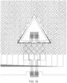
- Figure 11 illustrates a cut away section, for example only, of the glass substrate 140 and shows the shape and location of a through hole 225. This may have a slightly flattened circumferential edge region in one position. The flattened edge 1130 helps provide a run off point for electrodes which extend from the substrate over the transparent support.
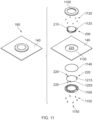
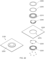
- the mounting collar 1420 comprises a lower collar member 1620 and an upper collar member 1630.
- the upper and lower collar members 1620, 1630 are made of metal, plastic, ceramic, composite or a combination thereof.
- the lower collar member 1620 is locatable proximate to the through hole on a lower surface of the touch panel 1405.
- the lower collar member 1620 comprises a number of separated ridge portions, which arc circumferentially to fit to an inner surface of the through hole in the touch panel 1405.
- the separated ridge portions provide a press fit type securement between the touch panel 1405 and the lower collar member 1620.
- a glue or resin may be added to the lower collar member for securing the lower collar member 1620 to the touch panel 1405. Spacings between the separated ridged portions of the lower collar member 1620 provide space for the tab portions 1610 when the lower collar member 1620 is secured to the touch panel 1405.
- the cross-section view (B) shows a securing element 1810 disposed partially within the user input button 1410. A further portion of the securing element 1820 is located in a recess of the mounting collar 1420, thereby securing the user input button 1410 to the mounting collar 1420.
- the user input button 1410 can be mounted to the mounting collar 1420 by positioning the user input button 1410 on the mounting collar 1420 with the hand actuated tool member 1820 to displace the securing element 1810, thereby locating and securing the securing element 1810 in a recess of the mounting collar 1820 as the elongate pin element of the hand actuated tool member 1820 is removed from the recess in the user input button 1410.
- the securing element 1810 includes a hooked end, which is biased towards the radially outer edge of the user input button 1410. Displacing the securing element 1810 with a pin of the hand actuated tool member 1820 urges the securing element radially inwards towards the centre of the user input button 1410.
- Power and/or data is provided to the combination device 2100 via electrodes in the touch panel 2205 to electrical contact pads 2270 extending into the through hole in the touch panel 2205.
- Each electrical contact pad 2270 may be connected to an end region of a plurality of electrodes in the touch panel.
- Figure 24 shows another example of providing power and/or data to electronic devices on the surface of a touch panel 2405.
- Electronic devices shown in the embodiment comprise a printed circuit board (PCB) 2410 including a plurality of addressable RBG LEDs arranged in an arc. Other arrangements of LEDs and different electronic devices may optionally be integrated on a surface of the touch panel 2405.
- the PCB 2410 comprises a number of electrical contact points that are soldered to electrical contact pads 2420 in the touch panel, each connected to an end region of at least one electrode 2430 in the touch panel for receiving power and/or data via the electrodes 2430 in touch panel. Three spaced apart arcs of different numbers of LEDs are shown in Figure 24 .
- a distal end region of the at least one electrode 2430 is connected to at least one electrical contact strip 2440.
- the electrical contact strip 2440 provides power and/or data from an external device to electronic devices on the touch panel via electrodes 2430 in the touch panel.
- Figure 25 illustrates an example electrical contact pad or strip 2510 of the embodiments described above.
- the electrical contact pad 2510 may be made of at least one tin-plated copper track on polyimide backing, with an end portion folded back on itself.
- the electrode pad 2510 may be provided on the same adhesive layer as electrodes of a touch panel 2520 described in embodiments disclosed above.
- a polyester layer 2530 may be provided over the adhesive layer and contact pad 2510. Folding back an end portion of the electrical contact pad 2510 of the present embodiment ensures that a tin-plated portion of the electrical contact pad abuts the polyester layer 2530.
- Connecting an electronic device to a contact pad 2510 requires soldering 2540, or other electrical connection process such as solder reflow or welding, to be used to remove part the polyester layer proximate to the electrical contact pad 2510.
- Figure 26 illustrates an example of a gaming machine 2600 including a touch 2605 panel and at least one combination device 2100 provided at the touch panel 2605.
- a plurality of combination devices, user input devices, electronic devices or a combination thereof may be provided at the touch panel 2605.
- a plurality of devices may be arranged at the touch panel 2605 of the gaming machine 2600 in order to allow multiple users to use the gaming machine 2600 simultaneously.
- the gaming machine 2600 is an information console.
- the gaming machine may be configured to receive information on user preferences via the touch panel 2605 and the at least one combination device 2100.
- Two combination devices are shown in Figure 26 and these are located at opposed ends of a central touch sensitive area where imagery is displayed as part of a game.
- Figure 27 illustrates a further example embodiment of a gaming machine 2700 that includes at least one touch panel 2705 in a first region of the gaming machine 2700.
- a further touch panel may be provided 2710 in a further region of the gaming machine 2700.
- combination devices 2100 are shown at the at least one touchscreen 2705.
- other types of combination device, user input device, and electronic device or a combination thereof may be provided at the at least one touch screen 2705.
- Electronic devices, for example LEDs 2310 may be provided at the further touch panel 2710.
- other types of electronic device, user input device, and combination device or a combination thereof may be provided at the further touch panel 2705.
- the gaming machine 2700 may also include other electronic devices such as lighting 2720, speakers, haptic and NFC devices in still further regions of the gaming machine 2700.
- the gaming machine 2700 is a kiosk or terminal that a user may use to access information or make purchases at a store.
Landscapes
- Engineering & Computer Science (AREA)
- General Engineering & Computer Science (AREA)
- Theoretical Computer Science (AREA)
- Human Computer Interaction (AREA)
- Physics & Mathematics (AREA)
- General Physics & Mathematics (AREA)
- Multimedia (AREA)
- Computer Networks & Wireless Communication (AREA)
- Position Input By Displaying (AREA)
- Push-Button Switches (AREA)
- Input From Keyboards Or The Like (AREA)
- Switches That Are Operated By Magnetic Or Electric Fields (AREA)
Claims (15)
- Procédé de fabrication d'un panneau tactile pour un écran tactile, comprenant les étapes de :tracé d'au moins un fil (430, 2310) comportant un diamètre de fil de 4 à 40 microns, sur une couche d'adhésif (235) sur un substrat transparent (230) qui comprend au moins un trou traversant (225), selon un motif prédéterminé qui comprend une première partie (435) qui s'étend sur le substrat et une partie supplémentaire qui s'étend sur une région d'un support transparent (240) qui s'étend sur au moins une région du trou traversant ;fourniture d'électrodes tactiles (300) pour un panneau tactile d'un écran tactile via la première partie du fil tracé (430) ; etfourniture d'une pluralité de connecteurs électriques (460) pour un dispositif d'entrée utilisateur (160, 1410, 2100) fixés au niveau du trou traversant, via la partie supplémentaire du fil tracé (430).
- Procédé selon la revendication 1, comprenant en outre :la fourniture du support transparent (240) en fournissant un film transparent sur une couche adhésive sur une première surface du substrat (230) ; moyennant quoile film transparent comportte un trou de film respectif sensiblement en concordance avec chaque trou traversant dans le substrat et une région de queue restante (450) qui s'étend sur la région du trou traversant (225).
- Procédé selon une quelconque des revendications précédentes, comprenant en outre :
la fixation d'une bande de connecteur flexible (280) qui comprend une pluralité de premières pastilles conductrices, aux connecteurs électriques, moyennant quoi chaque pastille est en connexion électrique respective avec au moins un connecteur électrique (460) ; et comprenant éventuellement en outre : la fixation d'une pluralité de pastilles conductrices supplémentaires de la bande de connecteur, chacune connectée à l'une respective des premières pastilles conductrices, à des contacts électriques respectifs (1610) du dispositif d'entrée utilisateur. - Procédé selon une quelconque des revendications précédentes, comprenant en outre :le tracé du fil (430) selon un motif moyennant quoi le fil qui fournit des électrodes tactiles est entrelacé avec le fil qui fournit un connecteur électrique ; et/oule tracé du fil (430) selon un motif moyennant quoi à chaque intersection, le fil qui fournit des électrodes tactiles croise le fil qui fournit un connecteur électrique de manière sensiblement orthogonale.
- Procédé selon une quelconque des revendications précédentes, comprenant en outre :
l'étape de fourniture d'électrodes tactiles (300) comprend la coupe d'un fil préalablement tracé en une pluralité d'emplacements pour fournir ainsi une pluralité d'électrodes tactiles X et Y ; et/ou l'étape de fourniture de connecteurs électriques (460) comprend la coupe d'un fil préalablement tracé en une pluralité d'emplacements pour fournir ainsi une pluralité de longueurs distinctes de fil qui s'étendent depuis une région de bord du substrat jusqu'à un emplacement sur le support transparent (250) à l'intérieur d'une limite imaginaire associée à un bord (400) d'un trou traversant (225) dans le substrat. - Procédé selon une quelconque des revendications précédentes, comprenant en outre :
la fourniture d'un dispositif d'entrée utilisateur (160, 1410, 2100) au niveau du trou traversant en fixant un bouton mécanique ou un joystick ou similaire au substrat (230) au niveau du trou traversant, moyennant quoi au moins un commutateur de contact (220, 1540) du dispositif d'entrée utilisateur est connecté électriquement à au moins un connecteur électrique fourni via la partie supplémentaire du fil tracé. - Panneau tactile (1405, 2205) pour un écran tactile, comprenant :une pluralité d'électrodes tactiles (300) fournies par des sections coupées d'au moins un fil tracé sur une couche d'adhésif sur un substrat transparent (230) qui comprend au moins un trou traversant (225) ;une pluralité de connecteurs électriques (460) fournis via des sections coupées d'au moins un fil tracé (430, 2310) sur ladite couche, dans lequel l'au moins un fil comporte un diamètre de 4 à 40 microns ; etau moins un dispositif d'entrée utilisateur (160, 1410, 2100), chacun fixé au niveau d'un trou traversant respectif (225) dans le substrat (230), dans lequel chaque dispositif d'entrée utilisateur comprend au moins un élément de commutation (220, 1540) connecté électriquement à au moins un dit connecteur électrique.
- Panneau tactile selon la revendication 7, comprenant en outre :
les électrodes tactiles (300) comprennent un premier groupe d'électrodes qui s'étendent à travers une région du substrat suivant un trajet répétitif constant et un groupe supplémentaire d'électrodes qui s'étendent à travers le substrat suivant le même trajet répétitif constant sur une partie de leur longueur mais qui comprend, à proximité d'un trou traversant, un trajet modifié autour d'un bord (245, 400) d'un trou traversant (225). - Panneau tactile selon la revendication 7 ou la revendication 8, comprenant en outre :
les connecteurs électriques (460) comprennent des sections tracées de fil (430, 2310) qui s'étendent sur l'adhésif à travers le substrat (230) et au-delà d'un bord (245, 400) d'un trou traversant (225) sur une région d'une couche d'adhésif (235) sur une région d'un support transparent (240) ; et éventuellement, chaque connecteur électrique comprend au moins une partie d'extrémité d'une ou plusieurs sections de fil tracé qui sont électriquement connectées à une pastille d'une bande de connecteur flexible (270, 280). - Panneau tactile selon l'une quelconque des revendications 7 à 9, comprenant en outre :un dispositif d'entrée utilisateur (160, 1410, 2100) au niveau de chaque trou traversant (225) dans le substrat, chaque dispositif d'entrée utilisateur comprenant un élément de façade (1100, 1520) au niveau d'une surface tactile (140) du substrat (230), un élément de base (1510) espacé de l'élément de façade mais fixé à celui-ci, un élément de déplacement par l'utilisateur (1440) entre l'élément de façade et l'élément de base lorsque l'élément de déplacement par l'utilisateur peut être déplacé par une main de l'utilisateur de l'écran tactile ; etau moins un élément de commutation (220, 1540), qui comporte un état sélectionnable par le mouvement de l'élément de déplacement par l'utilisateur, qui est en communication électrique, via au moins un connecteur électrique, avec un contrôleur du panneau tactile.
- Panneau tactile selon l'une quelconque des revendications 7 à 10, comprenant en outre :
le panneau tactile est conçu pour détecter des touchers via une zone active du panneau tactile et une entrée utilisateur supplémentaire via le déplacement d'un dispositif d'entrée utilisateur indiquant un choix de l'utilisateur. - Écran tactile (150), comprenant :un affichage ; etun panneau tactile (1405, 2205) selon l'une quelconque des revendications 7 à 11.
- Machine de jeu (100), jeu d'arcade, kiosque, guichet automatique ou panneau numérique comprenant l'écran tactile (150) selon la revendication 12.
- Bouton d'entrée utilisateur (160, 1410, 2100) pour un panneau tactile (1410, 2205) comprenant un substrat transparent (230) comprenant au moins un trou traversant (225), le bouton d'entrée utilisateur (160, 1410, 2100) étant adapté pour être fixé au niveau du trou traversant (225), comprenantun élément de façade (100, 1520) ;un élément de base (1510) ;un élément de déplacement par l'utilisateur (1440) entre l'élément de façade et l'élément de base ;au moins un élément de commutation (220, 1540) qui comporte un état sélectionnable par le déplacement de l'élément de déplacement par l'utilisateur ; etune bande de connecteur flexible (280) comprenant une pluralité de premières pastilles de contact (2010), au niveau d'une extrémité distale de la bande de connecteur flexible, pouvant être connectées à des connecteurs électriques fournis via un fil (430, 2310) tracé sur une couche adhésive (235) du panneau tactile, etdes pastilles de contact supplémentaires (1610) en communication électrique respective avec les premières pastilles de contact connectées à des fils qui s'étendent à travers le bouton d'entrée utilisateur pour connecter l'élément de commutation aux connecteurs électriques.
- Bouton d'entrée utilisateur selon la revendication 14, dans lequel l'élément de déplacement par l'utilisateur (1440) est un élément de bouton fabriqué à partir d'un matériau transparent ; et éventuellement, dans lequel l'élément de bouton est en verre ou en plastique et comporte une section transversale qui procure un effet de lentille.
Applications Claiming Priority (2)
| Application Number | Priority Date | Filing Date | Title |
|---|---|---|---|
| GBGB1816370.9A GB201816370D0 (en) | 2018-10-08 | 2018-10-08 | Button supply |
| PCT/GB2019/052830 WO2020074869A1 (fr) | 2018-10-08 | 2019-10-07 | Alimentation par boutons |
Publications (2)
| Publication Number | Publication Date |
|---|---|
| EP3864498A1 EP3864498A1 (fr) | 2021-08-18 |
| EP3864498B1 true EP3864498B1 (fr) | 2024-07-03 |
Family
ID=64394943
Family Applications (1)
| Application Number | Title | Priority Date | Filing Date |
|---|---|---|---|
| EP19787056.1A Active EP3864498B1 (fr) | 2018-10-08 | 2019-10-07 | Alimentation par boutons |
Country Status (9)
| Country | Link |
|---|---|
| US (1) | US11392215B2 (fr) |
| EP (1) | EP3864498B1 (fr) |
| JP (1) | JP7466215B2 (fr) |
| KR (1) | KR102709098B1 (fr) |
| CN (1) | CN113196215B (fr) |
| ES (1) | ES2992940T3 (fr) |
| GB (1) | GB201816370D0 (fr) |
| PT (1) | PT3864498T (fr) |
| WO (1) | WO2020074869A1 (fr) |
Families Citing this family (11)
| Publication number | Priority date | Publication date | Assignee | Title |
|---|---|---|---|---|
| KR102582641B1 (ko) * | 2018-11-30 | 2023-09-26 | 삼성디스플레이 주식회사 | 전자 패널 및 이를 포함하는 전자 장치 |
| KR102769392B1 (ko) | 2019-04-15 | 2025-02-20 | 삼성디스플레이 주식회사 | 전자 장치 |
| CN114171552B (zh) * | 2020-09-10 | 2025-09-09 | 京东方科技集团股份有限公司 | 显示基板及其制造方法和显示装置 |
| KR102721142B1 (ko) | 2021-07-06 | 2024-10-24 | 에스케이바이오사이언스(주) | 재배열 레오바이러스과 바이러스를 제조하는 방법 및 이를 위한 벡터 라이브러리 |
| GB2611350A (en) * | 2021-10-01 | 2023-04-05 | Zytronic Displays Ltd | An interactive device |
| CN115480657A (zh) * | 2022-09-05 | 2022-12-16 | 北京钛方科技有限责任公司 | 一种触控方法、触控装置和触控设备 |
| KR102813282B1 (ko) * | 2023-09-26 | 2025-05-28 | 포항공과대학교 산학협력단 | 2단자 연신성 터치 어레이 센서 및 그의 제조방법 |
| KR102945344B1 (ko) * | 2023-10-30 | 2026-04-01 | 주식회사 토비스 | 버튼장치 |
| KR102945345B1 (ko) | 2023-10-30 | 2026-04-01 | 주식회사 토비스 | 버튼장치 |
| US12248639B1 (en) * | 2023-11-15 | 2025-03-11 | Input Labs Oy | Human operable controller with touch sensor |
| CN119396291A (zh) * | 2024-11-13 | 2025-02-07 | 业桓科技(成都)有限公司 | 环状互动装置及人机交互系统 |
Family Cites Families (16)
| Publication number | Priority date | Publication date | Assignee | Title |
|---|---|---|---|---|
| US5936613A (en) * | 1993-11-05 | 1999-08-10 | Intertactile Technologies Corporation | Rotary circuit control devices with changeable graphics |
| US5805145A (en) * | 1993-11-05 | 1998-09-08 | Intertactile Technologies Corporation | Circuit control panel displaying changeable graphics |
| EP1389773A1 (fr) * | 1993-11-05 | 2004-02-18 | Intertactile Technologies Corporation | Interface opérateur/circuit à écran d'affichage intégré |
| JP5456450B2 (ja) * | 2009-12-01 | 2014-03-26 | インテレクチュアル ベンチャーズ ファンド 83 エルエルシー | 撮像装置及び操作装置 |
| DE102011108318A1 (de) * | 2011-07-22 | 2013-01-24 | Novomatic Ag | Elektronisches Spiel- und/oder Unterhaltungsgerät |
| GB2502594B (en) * | 2012-05-31 | 2016-10-26 | Zytronic Displays Ltd | Multi-touch sensing panel |
| GB2502601A (en) | 2012-05-31 | 2013-12-04 | Zytronic Displays Ltd | A touch sensitive panel made with individually insulated wires |
| US20160011633A1 (en) * | 2013-03-15 | 2016-01-14 | Sharp Kabushiki Kaisha | Electronic device |
| US9851605B2 (en) * | 2013-08-29 | 2017-12-26 | Sharp Kabushiki Kaisha | Display panel |
| CN106716580B (zh) * | 2014-11-10 | 2020-07-28 | 松下知识产权经营株式会社 | 输入装置 |
| US10437092B2 (en) * | 2015-08-18 | 2019-10-08 | Denso International America, Inc. | Projected display in control dial |
| FR3033423A1 (fr) * | 2015-09-17 | 2016-09-09 | Continental Automotive France | Afficheur avec systeme de decalage optique |
| WO2017130677A1 (fr) * | 2016-01-27 | 2017-08-03 | パナソニックIpマネジメント株式会社 | Dispositif d'entrée et système d'entrée |
| FR3050043B1 (fr) * | 2016-04-12 | 2019-06-14 | Visteon Global Technologies Inc | Dispositif d'interface composite avec un ecran tactile et un bouton de commande |
| WO2018109835A1 (fr) * | 2016-12-13 | 2018-06-21 | 三菱電機株式会社 | Bouton mécanique, dispositif d'affichage équipé d'un panneau tactile, et dispositif et procédé de commande de panneau tactile |
| GB201707478D0 (en) * | 2017-05-10 | 2017-06-21 | Zytronic Displays Ltd | Display arrangement |
-
2018
- 2018-10-08 GB GBGB1816370.9A patent/GB201816370D0/en not_active Ceased
-
2019
- 2019-10-07 EP EP19787056.1A patent/EP3864498B1/fr active Active
- 2019-10-07 KR KR1020217013940A patent/KR102709098B1/ko active Active
- 2019-10-07 JP JP2021543587A patent/JP7466215B2/ja active Active
- 2019-10-07 PT PT197870561T patent/PT3864498T/pt unknown
- 2019-10-07 CN CN201980066594.7A patent/CN113196215B/zh active Active
- 2019-10-07 US US17/283,155 patent/US11392215B2/en active Active
- 2019-10-07 ES ES19787056T patent/ES2992940T3/es active Active
- 2019-10-07 WO PCT/GB2019/052830 patent/WO2020074869A1/fr not_active Ceased
Also Published As
| Publication number | Publication date |
|---|---|
| KR20210088575A (ko) | 2021-07-14 |
| CN113196215A (zh) | 2021-07-30 |
| JP7466215B2 (ja) | 2024-04-12 |
| ES2992940T3 (en) | 2024-12-20 |
| CN113196215B (zh) | 2025-08-26 |
| KR102709098B1 (ko) | 2024-09-23 |
| WO2020074869A1 (fr) | 2020-04-16 |
| EP3864498A1 (fr) | 2021-08-18 |
| US20210349546A1 (en) | 2021-11-11 |
| GB201816370D0 (en) | 2018-11-28 |
| PT3864498T (pt) | 2024-08-26 |
| JP2022502808A (ja) | 2022-01-11 |
| US11392215B2 (en) | 2022-07-19 |
Similar Documents
| Publication | Publication Date | Title |
|---|---|---|
| EP3864498B1 (fr) | Alimentation par boutons | |
| CN203217512U (zh) | 系统和触敏设备 | |
| US11481057B2 (en) | Display arrangement | |
| EP3402075A1 (fr) | Électrode de détection de capacité comportant un dispositif d'entrée/sortie intégré | |
| EP3026534A1 (fr) | Dispositif d'écran tactile | |
| JP2022502808A5 (fr) | ||
| US8754870B2 (en) | Touch screen panel | |
| CN104793792A (zh) | 透光型输入装置 | |
| KR20110130298A (ko) | 터치 패널 일체형 액정 표시 장치 및 이의 제조 방법 | |
| KR20130111297A (ko) | 정전 용량식 입력 장치 | |
| GB2475253A (en) | A sheet with capacitive elements for input | |
| US11672080B2 (en) | Cursor control device with printed touch sensor | |
| CN213244063U (zh) | 一种后盖及电子设备 | |
| EP3486757B1 (fr) | Film et dispositif d'entrée | |
| KR20260044437A (ko) | 게임기용 조작 장치 및 이를 포함하는 게임기 | |
| JP5718047B2 (ja) | 光学式タッチパネル及び光学式タッチパネルの製造方法 | |
| JP2009028433A (ja) | スロットマシン |
Legal Events
| Date | Code | Title | Description |
|---|---|---|---|
| STAA | Information on the status of an ep patent application or granted ep patent |
Free format text: STATUS: UNKNOWN |
|
| STAA | Information on the status of an ep patent application or granted ep patent |
Free format text: STATUS: THE INTERNATIONAL PUBLICATION HAS BEEN MADE |
|
| PUAI | Public reference made under article 153(3) epc to a published international application that has entered the european phase |
Free format text: ORIGINAL CODE: 0009012 |
|
| STAA | Information on the status of an ep patent application or granted ep patent |
Free format text: STATUS: REQUEST FOR EXAMINATION WAS MADE |
|
| 17P | Request for examination filed |
Effective date: 20210423 |
|
| AK | Designated contracting states |
Kind code of ref document: A1 Designated state(s): AL AT BE BG CH CY CZ DE DK EE ES FI FR GB GR HR HU IE IS IT LI LT LU LV MC MK MT NL NO PL PT RO RS SE SI SK SM TR |
|
| DAV | Request for validation of the european patent (deleted) | ||
| DAX | Request for extension of the european patent (deleted) | ||
| STAA | Information on the status of an ep patent application or granted ep patent |
Free format text: STATUS: EXAMINATION IS IN PROGRESS |
|
| 17Q | First examination report despatched |
Effective date: 20220531 |
|
| GRAP | Despatch of communication of intention to grant a patent |
Free format text: ORIGINAL CODE: EPIDOSNIGR1 |
|
| STAA | Information on the status of an ep patent application or granted ep patent |
Free format text: STATUS: GRANT OF PATENT IS INTENDED |
|
| RIC1 | Information provided on ipc code assigned before grant |
Ipc: H01H 13/14 20060101ALN20240214BHEP Ipc: H01H 19/00 20060101ALI20240214BHEP Ipc: G06F 3/044 20060101ALI20240214BHEP Ipc: G06F 3/041 20060101ALI20240214BHEP Ipc: G06F 3/0362 20130101AFI20240214BHEP |
|
| INTG | Intention to grant announced |
Effective date: 20240228 |
|
| RIC1 | Information provided on ipc code assigned before grant |
Ipc: G06F 3/041 20060101ALI20240216BHEP Ipc: G06F 3/0362 20130101AFI20240216BHEP Ipc: H01H 13/14 20060101ALN20240216BHEP Ipc: H01H 19/00 20060101ALI20240216BHEP Ipc: G06F 3/044 20060101ALI20240216BHEP |
|
| GRAS | Grant fee paid |
Free format text: ORIGINAL CODE: EPIDOSNIGR3 |
|
| GRAA | (expected) grant |
Free format text: ORIGINAL CODE: 0009210 |
|
| STAA | Information on the status of an ep patent application or granted ep patent |
Free format text: STATUS: THE PATENT HAS BEEN GRANTED |
|
| AK | Designated contracting states |
Kind code of ref document: B1 Designated state(s): AL AT BE BG CH CY CZ DE DK EE ES FI FR GB GR HR HU IE IS IT LI LT LU LV MC MK MT NL NO PL PT RO RS SE SI SK SM TR |
|
| REG | Reference to a national code |
Ref country code: CH Ref legal event code: EP |
|
| REG | Reference to a national code |
Ref country code: DE Ref legal event code: R096 Ref document number: 602019054656 Country of ref document: DE |
|
| REG | Reference to a national code |
Ref country code: PT Ref legal event code: SC4A Ref document number: 3864498 Country of ref document: PT Date of ref document: 20240826 Kind code of ref document: T Free format text: AVAILABILITY OF NATIONAL TRANSLATION Effective date: 20240820 |
|
| REG | Reference to a national code |
Ref country code: NL Ref legal event code: FP |
|
| P01 | Opt-out of the competence of the unified patent court (upc) registered |
Free format text: CASE NUMBER: APP_45781/2024 Effective date: 20240807 |
|
| PGFP | Annual fee paid to national office [announced via postgrant information from national office to epo] |
Ref country code: GB Payment date: 20240911 Year of fee payment: 6 |
|
| REG | Reference to a national code |
Ref country code: LT Ref legal event code: MG9D |
|
| PGFP | Annual fee paid to national office [announced via postgrant information from national office to epo] |
Ref country code: NL Payment date: 20241011 Year of fee payment: 6 |
|
| PGFP | Annual fee paid to national office [announced via postgrant information from national office to epo] |
Ref country code: PT Payment date: 20241001 Year of fee payment: 6 |
|
| REG | Reference to a national code |
Ref country code: AT Ref legal event code: MK05 Ref document number: 1700511 Country of ref document: AT Kind code of ref document: T Effective date: 20240703 |
|
| REG | Reference to a national code |
Ref country code: ES Ref legal event code: FG2A Ref document number: 2992940 Country of ref document: ES Kind code of ref document: T3 Effective date: 20241220 |
|
| PGFP | Annual fee paid to national office [announced via postgrant information from national office to epo] |
Ref country code: DE Payment date: 20241010 Year of fee payment: 6 |
|
| PG25 | Lapsed in a contracting state [announced via postgrant information from national office to epo] |
Ref country code: NO Free format text: LAPSE BECAUSE OF FAILURE TO SUBMIT A TRANSLATION OF THE DESCRIPTION OR TO PAY THE FEE WITHIN THE PRESCRIBED TIME-LIMIT Effective date: 20241003 |
|
| PG25 | Lapsed in a contracting state [announced via postgrant information from national office to epo] |
Ref country code: FI Free format text: LAPSE BECAUSE OF FAILURE TO SUBMIT A TRANSLATION OF THE DESCRIPTION OR TO PAY THE FEE WITHIN THE PRESCRIBED TIME-LIMIT Effective date: 20240703 Ref country code: GR Free format text: LAPSE BECAUSE OF FAILURE TO SUBMIT A TRANSLATION OF THE DESCRIPTION OR TO PAY THE FEE WITHIN THE PRESCRIBED TIME-LIMIT Effective date: 20241004 Ref country code: PL Free format text: LAPSE BECAUSE OF FAILURE TO SUBMIT A TRANSLATION OF THE DESCRIPTION OR TO PAY THE FEE WITHIN THE PRESCRIBED TIME-LIMIT Effective date: 20240703 |
|
| PG25 | Lapsed in a contracting state [announced via postgrant information from national office to epo] |
Ref country code: BG Free format text: LAPSE BECAUSE OF FAILURE TO SUBMIT A TRANSLATION OF THE DESCRIPTION OR TO PAY THE FEE WITHIN THE PRESCRIBED TIME-LIMIT Effective date: 20240703 |
|
| PG25 | Lapsed in a contracting state [announced via postgrant information from national office to epo] |
Ref country code: LV Free format text: LAPSE BECAUSE OF FAILURE TO SUBMIT A TRANSLATION OF THE DESCRIPTION OR TO PAY THE FEE WITHIN THE PRESCRIBED TIME-LIMIT Effective date: 20240703 |
|
| PG25 | Lapsed in a contracting state [announced via postgrant information from national office to epo] |
Ref country code: IS Free format text: LAPSE BECAUSE OF FAILURE TO SUBMIT A TRANSLATION OF THE DESCRIPTION OR TO PAY THE FEE WITHIN THE PRESCRIBED TIME-LIMIT Effective date: 20241103 Ref country code: AT Free format text: LAPSE BECAUSE OF FAILURE TO SUBMIT A TRANSLATION OF THE DESCRIPTION OR TO PAY THE FEE WITHIN THE PRESCRIBED TIME-LIMIT Effective date: 20240703 |
|
| PGFP | Annual fee paid to national office [announced via postgrant information from national office to epo] |
Ref country code: FR Payment date: 20241010 Year of fee payment: 6 |
|
| PG25 | Lapsed in a contracting state [announced via postgrant information from national office to epo] |
Ref country code: HR Free format text: LAPSE BECAUSE OF FAILURE TO SUBMIT A TRANSLATION OF THE DESCRIPTION OR TO PAY THE FEE WITHIN THE PRESCRIBED TIME-LIMIT Effective date: 20240703 Ref country code: CZ Free format text: LAPSE BECAUSE OF FAILURE TO SUBMIT A TRANSLATION OF THE DESCRIPTION OR TO PAY THE FEE WITHIN THE PRESCRIBED TIME-LIMIT Effective date: 20240703 |
|
| PG25 | Lapsed in a contracting state [announced via postgrant information from national office to epo] |
Ref country code: RS Free format text: LAPSE BECAUSE OF FAILURE TO SUBMIT A TRANSLATION OF THE DESCRIPTION OR TO PAY THE FEE WITHIN THE PRESCRIBED TIME-LIMIT Effective date: 20241003 |
|
| PGFP | Annual fee paid to national office [announced via postgrant information from national office to epo] |
Ref country code: IT Payment date: 20241011 Year of fee payment: 6 Ref country code: ES Payment date: 20241115 Year of fee payment: 6 |
|
| PG25 | Lapsed in a contracting state [announced via postgrant information from national office to epo] |
Ref country code: RS Free format text: LAPSE BECAUSE OF FAILURE TO SUBMIT A TRANSLATION OF THE DESCRIPTION OR TO PAY THE FEE WITHIN THE PRESCRIBED TIME-LIMIT Effective date: 20241003 Ref country code: PL Free format text: LAPSE BECAUSE OF FAILURE TO SUBMIT A TRANSLATION OF THE DESCRIPTION OR TO PAY THE FEE WITHIN THE PRESCRIBED TIME-LIMIT Effective date: 20240703 Ref country code: NO Free format text: LAPSE BECAUSE OF FAILURE TO SUBMIT A TRANSLATION OF THE DESCRIPTION OR TO PAY THE FEE WITHIN THE PRESCRIBED TIME-LIMIT Effective date: 20241003 Ref country code: LV Free format text: LAPSE BECAUSE OF FAILURE TO SUBMIT A TRANSLATION OF THE DESCRIPTION OR TO PAY THE FEE WITHIN THE PRESCRIBED TIME-LIMIT Effective date: 20240703 Ref country code: IS Free format text: LAPSE BECAUSE OF FAILURE TO SUBMIT A TRANSLATION OF THE DESCRIPTION OR TO PAY THE FEE WITHIN THE PRESCRIBED TIME-LIMIT Effective date: 20241103 Ref country code: HR Free format text: LAPSE BECAUSE OF FAILURE TO SUBMIT A TRANSLATION OF THE DESCRIPTION OR TO PAY THE FEE WITHIN THE PRESCRIBED TIME-LIMIT Effective date: 20240703 Ref country code: GR Free format text: LAPSE BECAUSE OF FAILURE TO SUBMIT A TRANSLATION OF THE DESCRIPTION OR TO PAY THE FEE WITHIN THE PRESCRIBED TIME-LIMIT Effective date: 20241004 Ref country code: FI Free format text: LAPSE BECAUSE OF FAILURE TO SUBMIT A TRANSLATION OF THE DESCRIPTION OR TO PAY THE FEE WITHIN THE PRESCRIBED TIME-LIMIT Effective date: 20240703 Ref country code: CZ Free format text: LAPSE BECAUSE OF FAILURE TO SUBMIT A TRANSLATION OF THE DESCRIPTION OR TO PAY THE FEE WITHIN THE PRESCRIBED TIME-LIMIT Effective date: 20240703 Ref country code: BG Free format text: LAPSE BECAUSE OF FAILURE TO SUBMIT A TRANSLATION OF THE DESCRIPTION OR TO PAY THE FEE WITHIN THE PRESCRIBED TIME-LIMIT Effective date: 20240703 Ref country code: AT Free format text: LAPSE BECAUSE OF FAILURE TO SUBMIT A TRANSLATION OF THE DESCRIPTION OR TO PAY THE FEE WITHIN THE PRESCRIBED TIME-LIMIT Effective date: 20240703 |
|
| REG | Reference to a national code |
Ref country code: DE Ref legal event code: R097 Ref document number: 602019054656 Country of ref document: DE |
|
| PG25 | Lapsed in a contracting state [announced via postgrant information from national office to epo] |
Ref country code: SM Free format text: LAPSE BECAUSE OF FAILURE TO SUBMIT A TRANSLATION OF THE DESCRIPTION OR TO PAY THE FEE WITHIN THE PRESCRIBED TIME-LIMIT Effective date: 20240703 Ref country code: RO Free format text: LAPSE BECAUSE OF FAILURE TO SUBMIT A TRANSLATION OF THE DESCRIPTION OR TO PAY THE FEE WITHIN THE PRESCRIBED TIME-LIMIT Effective date: 20240703 Ref country code: DK Free format text: LAPSE BECAUSE OF FAILURE TO SUBMIT A TRANSLATION OF THE DESCRIPTION OR TO PAY THE FEE WITHIN THE PRESCRIBED TIME-LIMIT Effective date: 20240703 |
|
| PG25 | Lapsed in a contracting state [announced via postgrant information from national office to epo] |
Ref country code: EE Free format text: LAPSE BECAUSE OF FAILURE TO SUBMIT A TRANSLATION OF THE DESCRIPTION OR TO PAY THE FEE WITHIN THE PRESCRIBED TIME-LIMIT Effective date: 20240703 |
|
| PG25 | Lapsed in a contracting state [announced via postgrant information from national office to epo] |
Ref country code: SK Free format text: LAPSE BECAUSE OF FAILURE TO SUBMIT A TRANSLATION OF THE DESCRIPTION OR TO PAY THE FEE WITHIN THE PRESCRIBED TIME-LIMIT Effective date: 20240703 |
|
| PLBE | No opposition filed within time limit |
Free format text: ORIGINAL CODE: 0009261 |
|
| STAA | Information on the status of an ep patent application or granted ep patent |
Free format text: STATUS: NO OPPOSITION FILED WITHIN TIME LIMIT |
|
| REG | Reference to a national code |
Ref country code: CH Ref legal event code: PL |
|
| 26N | No opposition filed |
Effective date: 20250404 |
|
| PG25 | Lapsed in a contracting state [announced via postgrant information from national office to epo] |
Ref country code: MC Free format text: LAPSE BECAUSE OF FAILURE TO SUBMIT A TRANSLATION OF THE DESCRIPTION OR TO PAY THE FEE WITHIN THE PRESCRIBED TIME-LIMIT Effective date: 20240703 |
|
| PG25 | Lapsed in a contracting state [announced via postgrant information from national office to epo] |
Ref country code: LU Free format text: LAPSE BECAUSE OF NON-PAYMENT OF DUE FEES Effective date: 20241007 Ref country code: BE Free format text: LAPSE BECAUSE OF NON-PAYMENT OF DUE FEES Effective date: 20241031 |
|
| PG25 | Lapsed in a contracting state [announced via postgrant information from national office to epo] |
Ref country code: CH Free format text: LAPSE BECAUSE OF NON-PAYMENT OF DUE FEES Effective date: 20241031 |
|
| REG | Reference to a national code |
Ref country code: BE Ref legal event code: MM Effective date: 20241031 |
|
| PG25 | Lapsed in a contracting state [announced via postgrant information from national office to epo] |
Ref country code: SE Free format text: LAPSE BECAUSE OF FAILURE TO SUBMIT A TRANSLATION OF THE DESCRIPTION OR TO PAY THE FEE WITHIN THE PRESCRIBED TIME-LIMIT Effective date: 20240703 |
|
| PG25 | Lapsed in a contracting state [announced via postgrant information from national office to epo] |
Ref country code: IE Free format text: LAPSE BECAUSE OF NON-PAYMENT OF DUE FEES Effective date: 20241007 |
|
| PG25 | Lapsed in a contracting state [announced via postgrant information from national office to epo] |
Ref country code: CY Free format text: LAPSE BECAUSE OF FAILURE TO SUBMIT A TRANSLATION OF THE DESCRIPTION OR TO PAY THE FEE WITHIN THE PRESCRIBED TIME-LIMIT; INVALID AB INITIO Effective date: 20191007 |
|
| PG25 | Lapsed in a contracting state [announced via postgrant information from national office to epo] |
Ref country code: HU Free format text: LAPSE BECAUSE OF FAILURE TO SUBMIT A TRANSLATION OF THE DESCRIPTION OR TO PAY THE FEE WITHIN THE PRESCRIBED TIME-LIMIT; INVALID AB INITIO Effective date: 20191007 |