EP3865985B1 - Piezoelektrische messvorrichtung - Google Patents
Piezoelektrische messvorrichtung Download PDFInfo
- Publication number
- EP3865985B1 EP3865985B1 EP21156522.1A EP21156522A EP3865985B1 EP 3865985 B1 EP3865985 B1 EP 3865985B1 EP 21156522 A EP21156522 A EP 21156522A EP 3865985 B1 EP3865985 B1 EP 3865985B1
- Authority
- EP
- European Patent Office
- Prior art keywords
- voltage curve
- piezoelectric transducer
- touch
- control circuitry
- reference voltage
- Prior art date
- Legal status (The legal status is an assumption and is not a legal conclusion. Google has not performed a legal analysis and makes no representation as to the accuracy of the status listed.)
- Active
Links
Images


Classifications
-
- H—ELECTRICITY
- H10—SEMICONDUCTOR DEVICES; ELECTRIC SOLID-STATE DEVICES NOT OTHERWISE PROVIDED FOR
- H10N—ELECTRIC SOLID-STATE DEVICES NOT OTHERWISE PROVIDED FOR
- H10N30/00—Piezoelectric or electrostrictive devices
- H10N30/80—Constructional details
- H10N30/802—Circuitry or processes for operating piezoelectric or electrostrictive devices not otherwise provided for, e.g. drive circuits
-
- G—PHYSICS
- G06—COMPUTING OR CALCULATING; COUNTING
- G06F—ELECTRIC DIGITAL DATA PROCESSING
- G06F3/00—Input arrangements for transferring data to be processed into a form capable of being handled by the computer; Output arrangements for transferring data from processing unit to output unit, e.g. interface arrangements
- G06F3/01—Input arrangements or combined input and output arrangements for interaction between user and computer
- G06F3/03—Arrangements for converting the position or the displacement of a member into a coded form
- G06F3/041—Digitisers, e.g. for touch screens or touch pads, characterised by the transducing means
- G06F3/043—Digitisers, e.g. for touch screens or touch pads, characterised by the transducing means using propagating acoustic waves
-
- G—PHYSICS
- G06—COMPUTING OR CALCULATING; COUNTING
- G06F—ELECTRIC DIGITAL DATA PROCESSING
- G06F3/00—Input arrangements for transferring data to be processed into a form capable of being handled by the computer; Output arrangements for transferring data from processing unit to output unit, e.g. interface arrangements
- G06F3/01—Input arrangements or combined input and output arrangements for interaction between user and computer
- G06F3/03—Arrangements for converting the position or the displacement of a member into a coded form
- G06F3/041—Digitisers, e.g. for touch screens or touch pads, characterised by the transducing means
- G06F3/0414—Digitisers, e.g. for touch screens or touch pads, characterised by the transducing means using force sensing means to determine a position
-
- G—PHYSICS
- G06—COMPUTING OR CALCULATING; COUNTING
- G06F—ELECTRIC DIGITAL DATA PROCESSING
- G06F3/00—Input arrangements for transferring data to be processed into a form capable of being handled by the computer; Output arrangements for transferring data from processing unit to output unit, e.g. interface arrangements
- G06F3/01—Input arrangements or combined input and output arrangements for interaction between user and computer
- G06F3/03—Arrangements for converting the position or the displacement of a member into a coded form
- G06F3/041—Digitisers, e.g. for touch screens or touch pads, characterised by the transducing means
- G06F3/0416—Control or interface arrangements specially adapted for digitisers
-
- H—ELECTRICITY
- H03—ELECTRONIC CIRCUITRY
- H03K—PULSE TECHNIQUE
- H03K17/00—Electronic switching or gating, i.e. not by contact-making and –breaking
- H03K17/94—Electronic switching or gating, i.e. not by contact-making and –breaking characterised by the way in which the control signals are generated
- H03K17/96—Touch switches
- H03K17/964—Piezoelectric touch switches
-
- H—ELECTRICITY
- H10—SEMICONDUCTOR DEVICES; ELECTRIC SOLID-STATE DEVICES NOT OTHERWISE PROVIDED FOR
- H10N—ELECTRIC SOLID-STATE DEVICES NOT OTHERWISE PROVIDED FOR
- H10N30/00—Piezoelectric or electrostrictive devices
- H10N30/20—Piezoelectric or electrostrictive devices with electrical input and mechanical output, e.g. functioning as actuators or vibrators
-
- H—ELECTRICITY
- H10—SEMICONDUCTOR DEVICES; ELECTRIC SOLID-STATE DEVICES NOT OTHERWISE PROVIDED FOR
- H10N—ELECTRIC SOLID-STATE DEVICES NOT OTHERWISE PROVIDED FOR
- H10N30/00—Piezoelectric or electrostrictive devices
- H10N30/30—Piezoelectric or electrostrictive devices with mechanical input and electrical output, e.g. functioning as generators or sensors
-
- G—PHYSICS
- G06—COMPUTING OR CALCULATING; COUNTING
- G06F—ELECTRIC DIGITAL DATA PROCESSING
- G06F2203/00—Indexing scheme relating to G06F3/00 - G06F3/048
- G06F2203/041—Indexing scheme relating to G06F3/041 - G06F3/045
- G06F2203/04105—Pressure sensors for measuring the pressure or force exerted on the touch surface without providing the touch position
-
- G—PHYSICS
- G06—COMPUTING OR CALCULATING; COUNTING
- G06F—ELECTRIC DIGITAL DATA PROCESSING
- G06F3/00—Input arrangements for transferring data to be processed into a form capable of being handled by the computer; Output arrangements for transferring data from processing unit to output unit, e.g. interface arrangements
- G06F3/01—Input arrangements or combined input and output arrangements for interaction between user and computer
- G06F3/016—Input arrangements with force or tactile feedback as computer generated output to the user
Definitions
- the present disclosure relates to a device, and more particularly to an electronic device for sensing and/or for providing a haptic effect.
- Piezoelectric transducers may be used to provide haptic effects for a user, to sense touch, or both.
- performing both functionalities using a single piezoelectric transducer may present various challenges.
- the signal produced by the touch of a user may be difficult to detect if the piezoelectric transducer is driven with a driving voltage at the same time.
- Publication US 2009/146533 A1 discloses a system and method for measuring absolute pressure applied to a piezoelectric element by measuring a transition time of a voltage pulse applied to a piezoelectric element.
- the transition time is affected by the capacitance of the piezoelectric element, which in turn is affected by the amount of pressure currently being applied to the piezoelectric element.
- Publication US 9 965 930 B1 discloses an electronic device that may include a beam layer, a piezoelectric material layer coupled to the beam layer, and a temperature sensor adjacent the piezoelectric material layer.
- the electronic device may also include drive circuitry coupled to the piezoelectric material layer and configured to drive the piezoelectric material layer with a low frequency drive signal for actuating the piezoelectric material layer, and a high frequency drive signal for sensing a pressure applied to the piezoelectric material layer.
- Publication US 2011/128250 A1 discloses a method and a device for detecting user input that includes receiving a user input at an input arrangement of a user interface.
- the input arrangement has at least one piezoelectric sensor that generates an electric signal in response to the input.
- the electric signal is processed to determine the presence of the input.
- the processing may indicate the magnitude of the force of the input, in addition to the input's location.
- a device comprises: a touch surface; a piezoelectric transducer mechanically coupled to the touch surface; and a control circuitry electrically coupled to the piezoelectric transducer, configured to: drive the piezoelectric transducer using a test driving voltage; measure a response voltage curve caused by the test driving voltage over the piezoelectric transducer; calculate at least one parameter based on the response voltage curve; obtain the at least one parameter describing a reference response of the piezoelectric transducer; form a reference voltage curve based on the at least one parameter; drive the piezoelectric transducer with a driving voltage; measure a voltage curve over the piezoelectric transducer; compare the reference voltage curve and the measured voltage curve; and detect a touch on the touch surface based on the comparison.
- the device may, for example, be able to detect the touch on the touch surface even when driving the piezoelectric transducer with the driving voltage.
- control circuitry is further configured to detect a temporal change property of the touch on the touch surface based on the comparison.
- the device may, for example, be able to detect whether a force applied by the touch is increasing or decreasing.
- the at least one parameter comprises an RC time constant of the piezoelectric transducer.
- the device may, for example, be able to form the reference voltage curve using a single parameter.
- control circuitry is further configured to compare the reference voltage curve and the measured voltage curve by calculating a difference between the reference voltage curve and the measured voltage curve.
- the device may, for example, be able to efficiently compare the reference voltage curve and the measured voltage curve.
- control circuitry is further configured to compare the reference voltage curve and the measured voltage curve by: subtracting the reference voltage curve from the measured voltage curve producing a difference voltage curve; and detecting the touch based on the difference voltage curve.
- the device may, for example, detect the touch even when driving the piezoelectric transducer.
- control circuitry is further configured to: calculate an integral of the difference voltage curve; and detect the touch based on the integral of the difference voltage curve.
- the device may, for example, be able to detect the touch efficiently.
- control circuitry is further configured to: calculate a vibrational amplitude of the difference voltage curve; and detect the touch based on the vibrational amplitude of the difference voltage curve.
- the device may, for example, be able to detect the touch efficiently using the vibration induced by an object.
- control circuitry is further configured to compare the reference voltage curve and the measured voltage curve by: detecting a saturation period of the reference voltage curve; detecting a saturation period of the measured voltage curve; and comparing the saturation period of the reference voltage curve and of the measured voltage curve.
- the device may, for example, be able to detect the touch efficiently even when saturation limits the detection of the signals.
- a method comprises: driving a piezoelectric transducer using a test driving voltage; measuring a response voltage curve caused by the test driving voltage over the piezoelectric transducer; calculating at least one parameter based on the response voltage curve; obtaining the at least one parameter describing a reference response of the piezoelectric transducer; forming a reference voltage curve based on the at least one parameter; driving the piezoelectric transducer with a driving voltage; measuring a voltage curve over the piezoelectric transducer; comparing the reference voltage curve and the measured voltage curve; and detecting a touch on a touch surface based on the comparison.
- the detecting the touch on a touch surface based on the comparison comprises: detecting a temporal change property of the touch on the touch surface based on the comparison.
- the comparing the reference voltage curve and the measured voltage curve comprises subtracting the reference voltage curve from the measured voltage curve producing a difference voltage curve; and the detecting a touch on a touch surface based on the comparison comprises detecting the touch based on the difference voltage curve.
- the method further comprises: calculating an integral of the difference voltage curve; wherein the detecting a touch on a touch surface based on the comparison comprises detecting the touch based on the integral of the difference voltage curve.
- a computer program product comprising program code configured to perform a method according to the second aspect when the computer program is executed on a computing device.
- a disclosure in connection with a described method may also hold true for a corresponding device or system configured to perform the method and vice versa.
- a corresponding device may include a unit to perform the described method step, even if such unit is not explicitly described or illustrated in the figures.
- a corresponding method may include a step performing the described functionality, even if such step is not explicitly described or illustrated in the figures.
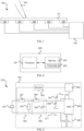
- Fig. 1 illustrates a schematic representation of a cross section of a device 100 according to an embodiment.
- the device 100 may comprise a touch surface 101.
- the touch surface 101 may also be referred to as a layer, a surface layer, a touch interface surface, or a touch interface layer.
- the touch surface 101 may be part of a touch user interface.
- the touch surface 101 may be, for example, a part of a trackpad or a key/button of a laptop computer or a touch screen.
- the touch surface 101 may comprise a first side and a second side.
- the first side may be at least partially unobstructed.
- a user may touch the first side with an object 104, such as a finger.
- the device 100 may further comprise a piezoelectric transducer 102.
- the piezoelectric transducer 102 may be mechanically coupled to the touch surface 101.
- two elements being mechanically coupled may indicate that there is a mechanical connection between the two elements.
- the two elements may be, for example, in contact with each other or the mechanical connection may be implemented via other elements.
- the piezoelectric transducer 102 may be in contact with the touch surface 101 or there may be one or more other elements between the piezoelectric transducer 102 and the touch surface 101.
- the force may be transferred to the piezoelectric transducer 102.
- the device 100 may further comprise a control circuitry 103 electrically coupled to the piezoelectric transducer 102.
- the control circuitry 103 may be configured to obtain at least one parameter describing a reference response of the piezoelectric transducer 102.
- the reference response may also be referred to as reference behaviour or similar.
- the reference response may describe how the piezoelectric transducer 102 responds when it is driven with a preconfigured signal/voltage, such as a preconfigured reference signal/voltage.
- the reference response may correspond to a time dependent voltage over the piezoelectric transducer 102 when the piezoelectric transducer 102 is driven with a preconfigured signal/voltage, such as a preconfigured reference signal/voltage.
- the at least one parameter may correspond to a reference response of the piezoelectric transducer 102.
- the at least one parameter may comprise, for example, an RC time constant of the piezoelectric transducer 102.
- the at least one parameter may comprise any other parameter describing the reference response of the piezoelectric transducer 102, such as resistance R of the piezoelectric transducer 102, capacitance C of the piezoelectric transducer 102, and/or at least one mechanical property of the piezoelectric transducer 102 and/or of the touch surface 101, such as stiffness of the touch surface 101 and/or stiffness of the piezoelectric transducer 102.
- the control circuitry 103 may be further configured to form a reference voltage curve based on the at least one parameter.
- the control circuitry 103 may form an RC voltage discharge curve of the piezoelectric transducer 102.
- the at least one parameter may comprise a plurality of parameters.
- the control circuitry 103 may be configured to form a more complex reference voltage curve.
- the control circuitry 103 may be configured to generate the reference voltage curve based on the at least one parameter.
- the control circuitry 103 may be configured to synthesize the reference voltage curve based on the at least one parameter.
- voltage curve may refer to a voltage that is a function of time.
- a voltage curve may be continuous or discrete.
- a voltage curve may be expressed using, for example, a mathematical expression that may be a function of time or using a plurality of discrete voltage samples.
- the control circuitry 103 may further be configured to drive the piezoelectric transducer with a driving voltage.
- the driving voltage may also be referred to as a driving voltage curve.
- the driving voltage may be a function of time.
- the driving voltage may comprise, for example, a voltage pulse.
- the voltage pulse may be, for example a substantially Gaussian voltage pulse.
- the control circuitry 103 may further be configured to measure a voltage curve over the piezoelectric transducer. This may produce a measured voltage curve.
- the control circuitry 103 may comprise at least one resistor electrically connected to the piezoelectric transducer 102.
- the at least one resistor may discharge the piezoelectric transducer 102.
- the control circuitry 103 may be configured to measure the voltage curve over the piezoelectric transducer 102 while the piezoelectric transducer 102 discharges via the at least one resistor.
- the control circuitry 103 may further be configured to compare the reference voltage curve and the measured voltage curve. This may produce a comparison result.
- the control circuitry 103 may compare the reference voltage curve and the measured voltage curve by, for example, subtracting the reference voltage curve from the measured voltage curve or vice versa.
- the control circuitry 103 may further be configured to detect a touch on the touch surface 101 based on the comparison.
- the control circuitry 103 may be configured to detect a touch on the touch surface 101 based on the comparison result.
- the piezoelectric transducer 102 may be arranged onto the second side of the surface 101.
- the device 100 may comprise a plurality of piezoelectric transducers 102. The disclosure herein may be applied for each piezoelectric transducer 102 in the plurality of piezoelectric transducers.
- the control circuitry 103 may be configured to deduce the location of the object 104 on the touch surface 101 based on the force detected in each piezoelectric transducer 102.
- the control circuitry 103 may perform this using, for example, a weighted average or a similar procedure.
- the piezoelectric transducers 102 may be next to the second side, in a close proximity of the second side or situated at a distance from the second side.
- Each piezoelectric transducer 102 in the plurality of piezoelectric transducers may be configured to convert a mechanical stress in the piezoelectric transducer 102 induced by a force exerted onto the first side of the touch surface 101 by an object 104 into a voltage.
- the mechanical stress may also be referred to as stress.
- the voltage may be referred to as electrical voltage, a stress induced voltage, or a corresponding voltage.
- the voltage may be proportional to the mechanical stress.
- the piezoelectric transducer 102 may be configured to convert the mechanical stress into the voltage via the piezoelectric effect, also referred to as piezoelectricity.
- the object 104 may be, for example, a finger of a user, any other body part of a human, a stylus pen, or some other object held by a user. In the case that the object 104 is a finger, the user may be wearing gloves, and only the fabric of the glove may be in direct contact with the touch surface 101.
- the voltage induced over the piezoelectric transducer 102, and therefore the measured voltage curve, may be proportional to the rate of change of the force/pressure applied by the object 104 to the touch surface 101.
- the piezoelectric transducer 102 may also be configured to convert a voltage applied over the piezoelectric transducers into a mechanical stress via the piezoelectric effect. Thus, when a driving voltage is applied over a piezoelectric transducer 102, a haptic effect may be induced into the touch surface 101.
- any embodiment of the device 100 described herein may be configured to locate the position of each object of a plurality of objects 104 on the touch surface 101. The positioning of each object 104 may be performed as described herein.
- Fig. 2 illustrates a schematic representation of a computing unit 200 according to an embodiment.
- the control circuitry 103 may comprise the computing unit 200.
- the computing unit 200 may comprise at least one processor 201.
- the at least one processor 201 may comprise, for example, one or more of various processing devices, such as a co-processor, a microprocessor, a digital signal processor (DSP), a processing circuitry with or without an accompanying DSP, or various other processing devices including integrated circuits such as, for example, an application specific integrated circuit (ASIC), a field programmable gate array (FPGA), a microprocessor unit (MCU), a hardware accelerator, a special-purpose computer chip, or the like.
- various processing devices such as a co-processor, a microprocessor, a digital signal processor (DSP), a processing circuitry with or without an accompanying DSP, or various other processing devices including integrated circuits such as, for example, an application specific integrated circuit (ASIC), a field programmable gate array (FPGA), a microprocessor unit (MCU), a hardware accelerator, a special-purpose computer chip, or the like.
- ASIC application specific integrated circuit
- the computing unit 200 may further comprise a memory 202.
- the memory may be configured to store, for example, computer programs and the like.
- the memory may comprise one or more volatile memory devices, one or more non-volatile memory devices, and/or a combination of one or more volatile memory devices and non-volatile memory devices.
- the memory may be embodied as magnetic storage devices (such as hard disk drives, floppy disks, magnetic tapes, etc.), optical magnetic storage devices, and semiconductor memories (such as mask ROM, PROM (programmable ROM), EPROM (erasable PROM), flash ROM, RAM (random access memory), etc.).
- some component and/or components of the computing unit 200 such as the at least one processor and/or the memory, may be configured to implement this functionality.
- this functionality may be implemented using program code comprised, for example, in the memory.
- the memory 202 may comprise the at least one parameter 203.
- the computing unit 200 may further comprise, for example, a boost converter circuit, a microprocessor, and other components used to interact with the piezoelectric transducers 102.
- the boost converter may provide a high voltage that may be needed to drive the piezoelectric transducers 102 in the case of haptic feedback.
- the computing unit 200 may be configured to perform that computational operation.
- a computation operation may comprise, for example, obtaining at least one parameter, forming the reference voltage curve based on the at least one parameter, comparing the reference voltage curve and the measured voltage curve, and/or detecting a touch on the touch surface based on the comparison.
- Fig. 3 illustrates a circuit diagram representation of a device 100 according to an embodiment.
- control circuitry 103 may refer to various components in the device 100 that are used to control the piezoelectric transducer 102.
- the piezoelectric transducer 102 may be modelled as a capacitor.
- Other electrical/physical properties, such as resistance, inductance, hysteresis, and LC resonance, of the piezoelectric transducer 102 may also be modelled by adding corresponding electrical components to the model of the piezoelectric transducer 102.
- a resistor may be added to model the resistive losses in the piezoelectric transducer 102.
- An inductor may be added to model the inductance of the piezoelectric transducer 102. In many cases the capacitive behaviour of the piezoelectric transducer 102 may be dominant, and therefore modelling the piezoelectric transducer 102 as a single capacitor may be sufficient.
- the device 100 may comprise a voltage divider 303 comprising a first 301 and a second resistor 302.
- the device 100 may further comprise a low-pass filter 306 comprising a third resistor 304 and a capacitor 305.
- the low-pass filter 306 may be configured to filter out unwanted frequency components.
- a cut-off frequency of the low-pass filter 306 may be, for example, in the range 50 - 300 hertz (Hz), or in any subrange of this, such as 50 - 200 Hz, 50 - 150 Hz, or 70 - 130 Hz.
- the device 100 may further comprise a first 307 and a second diode 308.
- the device 100 may further comprise an analogue to digital converter (ADC) 309.
- ADC analogue to digital converter
- the control circuitry 103 may for example comprise the ADC 309.
- the first 307 and second diode 308 may limit the voltage fed into the ADC 309.
- the first diode 307 may be coupled between a first conductor 310 and a maximum voltage V max .
- the second diode 308 may be coupled between the first conductor 310 and a minimum voltage - V max .
- the first conductor 310 may be electrically coupled to the ADC 309.
- the voltage fed into the ADC 309 via the first conductor 310 may be limited between - V max and + V max .
- the dynamic range of the ADC 309 may be 2 V max .
- the control circuitry 103 may further comprise a reference voltage circuit 330.
- the reference voltage circuit 330 may provide a reference voltage V ref .
- the ADC 309 may be electrically coupled to a second conductor 311.
- the second conductor 311 may be at the reference voltage V ref .
- the reference voltage may correspond to, for example, a ground voltage, 1 / 2V dd , or similar.
- V dd may be a power supply voltage.
- the ADC 309 may be configured to measure a voltage between the first conductor 310 and the second conductor 311.
- V ref may comprise any practical voltage within the dynamic range of the ADC 309, which allows reading of piezo voltages above and below V ref .
- V ref does not need to be in the centre of the dynamic range of the ADC 309, nor does the response above/below need to be linear, or with similar dynamics above/below. However, there may need to be a capability to measure into both directions, differentially in relation to V ref .
- V ref may correspond to a ground voltage.
- the ADC 309 may need to be capable of reading also negative voltages, which may increase manufacturing costs of the device 100.
- the device 100 may further comprise other components not illustrated in the figures.
- the device 100 may comprise a multiplexer.
- a plurality of piezoelectric transducer 102 may be coupled to the ADC 309 via the multiplexer.
- the device 100 may further comprise a boost converter 320.
- the boost converter 320 may be configured to drive the piezoelectric transducer 102.
- the computing unit 200 may be electrically coupled to a boost converter 320 and the computing unit 200 may control the boost converter 320 so that the boost converter 320 provides the driving voltage/current for the piezoelectric transducer 102.
- the boost converter 320 may drive a plurality of piezoelectric transducers 102 via a multiplexer.
- the boost converter 320 and the sensing circuitry may be always connected to the piezoelectric transducer 102 without the need to switch between sensing and haptic driving. This may enable high responsiveness and improved usability.
- each terminal of the piezoelectric transducer 102 may be at a reference voltage V ref .
- the reference voltage may be selected according to the sensing system at hand. In the idle state, this voltage may remain substantially constant. Thus, there may be no voltage over the first resistor 301 and/or the second resistor 302.
- the terminal of the piezoelectric transducer 102 connected to the first resistor 301 may be referred to as a measuring terminal.
- the terminal of the piezoelectric transducer 102 connected to the second conductor 311 may be referred to as a reference terminal.
- the potential difference can introduce a current through first resistor 301 and the second resistor 302, and the current discharges the electric charge in piezoelectric transducer 102.
- This can be detected by the control circuitry 103 as a voltage over the second resistor 302.
- the voltage may comprise a RC discharge curve due to the resistance of the piezoelectric transducer 102 and of the first 301 and the second resistor 302 and due to the capacitance of the piezoelectric transducer 102.
- the resistance of the first 301 and second 302 resistor may dominate the internal resistance of the piezoelectric transducer 102. Resistance of the first 301 and second 302 resistor may be chosen so that they produce a reasonable decay rate of the voltage over the piezoelectric transducer 102 for human interface purposes.
- the device 100 may comprise a computing unit 200.
- the control circuitry 103 may comprise the computing unit 200.
- the computing unit 200 may be electrically coupled to the boost converter 320 and/or to the ADC 309.
- the computing unit 200 may obtain voltage measurement samples via the ADC 309.
- the computing unit 200 may also control the boost converter 320.
- the boost converter 320 is configured to perform some operation, the computing unit 200 may be configured to perform that operation by controlling the boost converter 320.
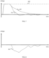
- Fig. 4 illustrates a schematic representation of a driving voltage 402 used to drive a piezoelectric transducer 102 and a reference voltage curve 401 according to an embodiment.
- the scale of the driving voltage 402 and of the reference voltage curve 401 may not be the same.
- the amplitude of the driving voltage 402 may be in the range 50 - 500 volts (V), or in any subrange of this, such as 50 - 300 V, 100 - 300 V, or 150 - 250 V.
- the maximum of the reference voltage curve 401 may be limited by a saturation voltage level 403.
- the saturation voltage level 403 may be less than 10 V, for example 3.3 V.
- the saturation voltage level 403 may be due to, for example, the limited dynamic range of the ADC 309.
- the reference voltage curve 401 may correspond to the driving voltage 402.
- the reference voltage curve 401 may correspond to the voltage over the piezoelectric transducer 102 when the piezoelectric transducer 102 is not touched by an object 104.
- the control circuitry 103 may form the reference voltage curve 401 based on the at least one parameter 203.
- the at least one parameter 203 comprises an RC constant ⁇ of the piezoelectric transducer 102
- R may be the resistance of the piezoelectric transducer 102 and C may be the capacitance of the piezoelectric transducer 102.
- the resistance R may also comprise the resistance of the first 301 and/or second resistor 302.
- ⁇ may be, for example, 5 - 10 milliseconds (ms).
- the reference voltage curve 401 may saturate as illustrated in the embodiment of Fig. 4 .
- the reference voltage curve 401 may follow the behaviour described above only when the reference voltage curve 401 is not saturated.
- components other than the piezoelectric transducer 102 may affect the reference voltage curve and/or the at least one parameter.
- some components may comprise capacitance which may affect the reference voltage curve 401 and/or the at least one parameter 203.
- the at least one parameter 203 may comprise an RC time constant of a circuit comprising the piezoelectric transducer 102.
- Fig. 5 illustrates a schematic representation of a measured voltage curve 501 over a piezoelectric transducer 102 according to an embodiment.
- the measured voltage curve 501 presented in the embodiment of Fig. 5 may correspond to a situation when an object 104 touching the touch surface 101 is reducing the pressing force. This may be observed as a difference between the reference voltage curve 401 and the measured voltage curve 501. Due to the reducing force, the value of the measured voltage curve 501 is greater than the value of the reference voltage curve 401 when the force is reducing.
- the discussion herein may assume that the piezoelectric transducer 102 is reverse-polarised. If the piezoelectric transducer 102 is not reverse-polarised, the situation presented in the embodiment of Fig. 5 may correspond to a situation where pressing force is increased.
- the control circuitry 103 may further be configured to compare the reference voltage curve 401 and the measured voltage curve 501 by: detecting a saturation period 502 of the reference voltage curve 402, detecting a saturation period 503 of the measured voltage curve 501; and comparing the saturation period of the reference voltage curve 401 and of the measured voltage curve 501.
- saturation period may refer to the length of the time interval that the voltage curve in question is in saturation.
- a voltage curve may be in saturation when the value of the voltage curve is greater or equal to the saturation voltage level 403.
- the saturation period of the reference voltage curve 401 may refer to the length of the time interval t s,r 502 illustrated in the embodiment of Fig. 5 .
- the saturation period of the measured voltage curve 501 may refer to the length of the time interval t s,m 503 illustrated in the embodiment of Fig. 5 .
- the measured voltage curve 501 is in saturation for a shorter period of time than the reference voltage curve 401. This may correspond to a situation where the object 104 touching the touch surface 101 is increasing the pressing force.
- Fig. 6 illustrates a schematic representation of a difference voltage curve 601 according to an embodiment.
- the control circuitry 103 may be further configured to compare the reference voltage curve 401 and the measured voltage curve 501 by calculating a difference between the reference voltage 401 curve and the measured voltage curve 501.
- the control circuitry 103 may be further configured to compare the reference voltage curve 401 and the measured voltage curve 501 by subtracting the reference voltage curve 401 from the measured voltage curve 501 producing a difference voltage curve 601; and detecting the touch based on the difference voltage curve 601.
- the difference voltage curve illustrated in Fig. 6 may be obtained by subtracting the reference voltage curve 401 from the measured voltage curve 501 presented in Fig. 5 .
- the control circuitry 103 may be configured to detect sign/polarity of the difference voltage curve V diff ( t ). For example, in the case of the difference voltage curve 601 presented in Fig. 6 , the control circuitry 103 may be configured to detect that the difference voltage curve 601 is dominantly positive.
- the control circuitry 103 may be configured to detect a temporal change property of the touch based on the sign/polarity of the difference voltage curve V diff ( t ). For example, in the case of the difference voltage curve 601 presented in Fig. 6 , the control circuitry 103 may be configured to detect that the force applied by the touch is decreasing.
- the control circuitry 103 may be further configured to detect a temporal change property of the touch on the touch surface 101 based on the comparison.
- a temporal change property of the touch on the touch surface 101 may refer to any property of the touch changing in time.
- the control circuitry 103 may be configured to detect whether the force/pressure applied by the touch is increasing, decreasing, or remaining constant.
- the control circuitry 103 may be further configured to calculate an integral of the difference voltage curve and detect the touch based on the integral of the difference voltage curve.
- t 1 may be the time instant at which the device 100 starts to drive the piezoelectric transducer with the driving voltage.
- t 2 may be a preconfigured time instant after t 1 .
- the control circuitry 103 may deduce whether an object is touching the touch surface 101 or not. For example, in the case of the embodiment of Fig. 6 , V diff ( t ) is mostly positive. Thus, the result of the integral is positive, and control circuitry 103 can deduce that the object may be touching the touch surface 101 with a decreasing force.
- control circuitry 103 may use other methods to evaluate the value of the integral I .
- the control circuitry 103 may be configured to detect the touch on the touch surface 101 in response to the integral I reaching a preconfigured threshold value.
- the time resolution T / N may be, for example, less than 1 ms.
- T and/or N may comprise preconfigured values.
- the control circuitry 103 may be configured to sample the difference voltage curve until I reaches some preconfigured threshold value. In response to the preconfigured value being reached, the control circuitry 103 may detect the touch on the touch surface 101.
- control circuitry 103 is further configured to calculate a vibrational amplitude of the difference voltage curve and detect the touch based on the vibrational amplitude of the difference voltage curve.
- the object 104 may introduce a vibration into the touch surface 101. This vibration may be detected via the piezoelectric transducer 102.
- the average vibration amplitude A ave may quantify the amount of vibration in the piezoelectric transducer 102.
- the vibrational amplitude of the difference voltage may comprise the average vibration amplitude A ave .
- the computing unit 200 may use the vibrational component of each piezoelectric transducer 102 to calculate/estimate the position of the object 104 on the surface 101.
- the control circuitry 103 may, for example, compare the vibrational amplitude of the difference voltage to a preconfigured threshold. If the vibrational amplitude of the difference voltage is greater than the preconfigured threshold, the control circuitry 103 may deduce that an object 104 is touching the touch surface 101.
- Fig. 7 illustrates a schematic representation of a measured voltage curve 701 over a piezoelectric transducer 102 according to an embodiment.
- the measured voltage curve 701 presented in the embodiment of Fig. 7 may correspond to a situation where an object 104 touching the touch surface 101 is increasing the pressing force. This may be observed as a difference between the reference voltage curve 401 and the measured voltage curve 701. Due to the increasing force, the value of the measured voltage curve 701 is smaller than the value of the reference voltage curve 401 when the force is increasing.
- Fig. 8 illustrates a schematic representation of a difference voltage curve 801 according to an embodiment.
- the difference voltage curve 801 illustrated in Fig. 8 may be obtained by subtracting the reference voltage curve 401 from the measured voltage curve 701 presented in Fig. 7 .
- the control circuitry 103 may be configured to detect sign/polarity of the difference voltage curve V diff ( t ). For example, in the case of the difference voltage curve 801 presented in Fig. 8 , the control circuitry 103 may be configured to detect that the difference voltage curve 801 is dominantly negative.
- the control circuitry 103 may be configured to detect a temporal change property of the touch based on the sign/polarity of the difference voltage curve V diff ( t ). For example, in the case of the difference voltage curve 801 presented in Fig. 8 , the control circuitry 103 may be configured to detect that the force/pressure applied by the touch is increasing.
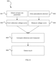
- Fig. 9 illustrates a flow chart representation of a method according to an embodiment.
- the method 900 comprises obtaining 901 at least one parameter describing a reference response of a piezoelectric transducer.
- the method 900 may further comprise forming 902 a reference voltage curve based on the at least one parameter.
- the method 900 may further comprise driving 903 the piezoelectric transducer with a driving voltage.
- the method 900 may further comprise measuring 904 a voltage curve over the piezoelectric transducer.
- the method 900 may further comprise comparing 905 the reference voltage curve and the measured voltage curve.
- the method 900 may further comprise detecting 906 a touch on a touch surface based on the comparison.
- Fig. 10 illustrates a flow diagram representation of voltages used by the control circuitry 103 according to an embodiment.
- the control circuitry 103 may further be configured to drive the piezoelectric transducer 102 using a test driving voltage 1001.
- the test driving voltage 1001 may be similar to the driving voltage 402.
- the test driving voltage 1001 may comprise, for example, any preconfigured voltage curve suitable for testing the electrical and/or mechanical properties of the piezoelectric transducer 102.
- the control circuitry 103 may be configured to drive the piezoelectric transducer 102 with the test driving voltage 1001 when there is no external force applied by an object 104 to the touch surface 101.
- the control circuitry 103 may further be configured to measure a response voltage curve 1002 caused by the test driving voltage 1001 over the piezoelectric transducer 102.
- control circuitry 103 may be configured to drive the piezoelectric transducer 102 with the test driving voltage 1001 when there is no external force applied by and object 104 to the touch surface 101, the response voltage curve 1002 may correspond to the reference voltage curve 402. Thus, the control circuitry 103 may obtain the reference voltage 402 curve by measuring the response voltage curve 1002.
- the control circuitry 103 may further be configured to calculate 1003 the at least one parameter 203 based on the response voltage curve 1002.
- the control circuitry 103 may further be configured to store the at least one parameter 203.
- the control circuitry 103 may store the at least one parameter 203 into, for example, the memory 202.
- the control circuitry 103 may, for example, estimate the RC time constant of the piezoelectric transducer 102 based on the response voltage curve 1002.
- the control circuitry 103 may use, for example, curve fitting and/or other computational procedures to obtain the at least one parameter 203 from the response voltage curve 1002.
- the control circuitry 103 may perform the aforementioned operations for calculating the at least one parameter 203, for example, periodically. Since the electrical and/or mechanical properties of the piezoelectric transducer 102 may change over time, the control circuitry 103 may this way update the at least one parameter 203 to correspond to the current properties of the piezoelectric transducer 102. Thus, the reference voltage curve 401 formed based on the at least one parameter 203 may more accurately describe the reference behaviour of the piezoelectric transducer 102.
- the control circuitry 103 may then obtain the at least one parameter 203, form the reference voltage curve 401 based on the at least one parameter 203, drive the piezoelectric transducer with a driving voltage 402, measure a voltage curve 501 over the piezoelectric transducer 102, compare the reference voltage curve 401 and the measured voltage curve 501 and detect a touch on the touch surface 101 based on the comparison as described herein.
Landscapes
- Engineering & Computer Science (AREA)
- General Engineering & Computer Science (AREA)
- Theoretical Computer Science (AREA)
- Physics & Mathematics (AREA)
- Human Computer Interaction (AREA)
- General Physics & Mathematics (AREA)
- Acoustics & Sound (AREA)
- User Interface Of Digital Computer (AREA)
- Electronic Switches (AREA)
- Apparatuses For Generation Of Mechanical Vibrations (AREA)
Claims (13)
- Vorrichtung (100), umfassend:eine Touch-Oberfläche (101);einen piezoelektrischen Wandler (102), der mechanisch mit der Berührungsfläche (101) gekoppelt ist; undeine Steuerschaltung (103), die elektrisch mit dem piezoelektrischen Wandler (102) gekoppelt ist, konfiguriert für:Ansteuern des piezoelektrischen Wandlers (102) unter Verwendung einer Testansteuerspannung (1001);Messen einer Ansprechspannungskurve (1002), die durch die Testansteuerspannung (1001) über dem piezoelektrischen Wandler (102) verursacht wird;Berechnen mindestens eines Parameters (203) basierend auf der Ansprechspannungskurve (1002);Erhalten des mindestens einen Parameters (203), der eine Referenzantwort des piezoelektrischen Wandlers (102) beschreibt;Bilden einer Referenzspannungskurve (401) auf der Grundlage des mindestens einen Parameters (203);Ansteuern des piezoelektrischen Wandlers (102) mit einer Ansteuerspannung (402);Messen einer Spannungskurve (501, 701) über den piezoelektrischen Wandler (102), nachdem der piezoelektrische Wandler (102) mit der Ansteuerspannung (402) angesteuert wurde;Vergleichen der Referenzspannungskurve (401) und der gemessenen Spannungskurve (501, 701); undDetektieren einer Berührung auf der Berührungsoberfläche (101) basierend auf dem Vergleich.
- Vorrichtung (100) nach Anspruch 1, wobei die Steuerschaltung (103) weiter konfiguriert ist, um:
Detektieren einer zeitlichen Änderungseigenschaft der Berührung auf der Berührungsoberfläche (101) basierend auf dem Vergleich. - Vorrichtung (100) nach Anspruch 1 oder Anspruch 2, wobei der mindestens eine Parameter (203) eine RC-Zeitkonstante des piezoelektrischen Wandlers (102) umfasst.
- Vorrichtung (100) nach einem vorhergehenden Ansprüche, wobei die Steuerschaltung (103) weiter konfiguriert ist, um die Referenzspannungskurve (401) und die gemessene Spannungskurve (501, 701) zu vergleichen, indem eine Differenz zwischen der Referenzspannungskurve (401) und der gemessenen Spannungskurve (501, 701) berechnet wird.
- Vorrichtung (100) nach einem vorhergehenden Ansprüche, wobei die Steuerschaltung (103) weiter konfiguriert ist, um die Referenzspannungskurve und die gemessene Spannungskurve zu vergleichen durch:Subtrahieren der Referenzspannungskurve (401) von der gemessenen Spannungskurve (501, 701), wodurch eine Differenzspannungskurve (601, 801) erzeugt wird; undErkennen der Berührung anhand der Differenzspannungskurve (601, 801).
- Vorrichtung (100) nach Anspruch 5, wobei die Steuerschaltung (103) weiter konfiguriert ist, um:Berechnen eines Integrals der Differenzspannungskurve (601, 801); undErkennen der Berührung basierend auf dem Integral der Differenzspannungskurve.
- Vorrichtung (100) nach Anspruch 5, wobei die Steuerschaltung (103) weiter konfiguriert ist, um:Berechnen einer Schwingungsamplitude der Differenzspannungskurve (601, 801); undErkennen der Berührung basierend auf der Schwingungsamplitude der Differenzspannungskurve.
- Vorrichtung (100) nach einem vorhergehenden Ansprüche, wobei die Steuerschaltung (103) weiter konfiguriert ist, um die Referenzspannungskurve und die gemessene Spannungskurve zu vergleichen durch:Erfassen einer Sättigungsperiode (502) der Referenzspannungskurve (401);Erfassen einer Sättigungsperiode (503) der gemessenen Spannungskurve (501, 701); undVergleich der Sättigungsperiode der Referenzspannungskurve und der gemessenen Spannungskurve.
- Verfahren (900), umfassend:Ansteuern eines piezoelektrischen Wandlers mit einer Testansteuerspannung;Messen einer Ansprechspannungskurve, die durch die Testansteuerspannung über den piezoelektrischen Wandler verursacht wird;Berechnen von mindestens einem Parameter auf der Grundlage der Ansprechspannungskurve;Erhalten (901) des mindestens einen Parameters, der eine Referenzantwort des piezoelektrischen Wandlers beschreibt;Bilden (902) einer Referenzspannungskurve auf der Grundlage des mindestens einen Parameters;Ansteuerung (903) des piezoelektrischen Wandlers mit einer Ansteuerspannung;Messen (904) eines Spannungsverlaufs über dem piezoelektrischen Wandler nach Ansteuerung des piezoelektrischen Wandlers mit einer Ansteuerspannung;Vergleichen (905) der Referenzspannungskurve und der gemessenen Spannungskurve; undErkennen (906) einer Berührung auf einer Berührungsoberfläche auf der Grundlage des Vergleichs.
- Verfahren (900) nach Anspruch 9, wobei das Erfassen der Berührung auf einer Berührungsoberfläche auf der Grundlage des Vergleichs umfasst:
Erkennen einer zeitlichen Änderungseigenschaft der Berührung auf der Berührungsoberfläche basierend auf dem Vergleich. - Verfahren (900) nach Anspruch 10 oder Anspruch 10, wobei das Vergleichen (905) der Referenzspannungskurve und der gemessenen Spannungskurve das Subtrahieren der Referenzspannungskurve von der gemessenen Spannungskurve umfasst, wodurch eine Differenzspannungskurve erzeugt wird; und
Das Erkennen (906) einer Berührung auf einer Berührungsoberfläche auf der Grundlage des Vergleichs umfassend das Erkennen der Berührung auf der Grundlage der Differenzspannungskurve. - Verfahren (900) nach Anspruch 11, ferner umfassend:Berechnen eines Integrals der Differenzspannungskurve;wobei das Erkennen (906) einer Berührung auf einer Berührungsoberfläche auf der Grundlage des Vergleichs das Erfassen der Berührung auf der Grundlage des Integrals der Differenzspannungskurve umfasst.
- Computerprogrammprodukt mit Programmcode, der so konfiguriert ist, dass er das Verfahren nach einem der Ansprüche 9 bis 12 ausführt, wenn der Programmcode auf einem Computer ausgeführt wird.
Applications Claiming Priority (1)
| Application Number | Priority Date | Filing Date | Title |
|---|---|---|---|
| FI20205146A FI20205146A1 (en) | 2020-02-12 | 2020-02-12 | PIETRO - ELECTRIC DEVICE |
Publications (2)
| Publication Number | Publication Date |
|---|---|
| EP3865985A1 EP3865985A1 (de) | 2021-08-18 |
| EP3865985B1 true EP3865985B1 (de) | 2024-07-17 |
Family
ID=74591829
Family Applications (1)
| Application Number | Title | Priority Date | Filing Date |
|---|---|---|---|
| EP21156522.1A Active EP3865985B1 (de) | 2020-02-12 | 2021-02-11 | Piezoelektrische messvorrichtung |
Country Status (5)
| Country | Link |
|---|---|
| US (1) | US11360609B2 (de) |
| EP (1) | EP3865985B1 (de) |
| JP (1) | JP7702256B2 (de) |
| CN (1) | CN113253869B (de) |
| FI (1) | FI20205146A1 (de) |
Family Cites Families (28)
| Publication number | Priority date | Publication date | Assignee | Title |
|---|---|---|---|---|
| JPS58182746A (ja) * | 1982-04-20 | 1983-10-25 | Fujitsu Ltd | タツチ式入力装置 |
| US7277087B2 (en) * | 2003-12-31 | 2007-10-02 | 3M Innovative Properties Company | Touch sensing with touch down and lift off sensitivity |
| JP4543863B2 (ja) | 2004-10-05 | 2010-09-15 | ソニー株式会社 | 触覚機能付きの入出力装置及び電子機器 |
| JP2008527557A (ja) * | 2005-01-14 | 2008-07-24 | コーニンクレッカ フィリップス エレクトロニクス エヌ ヴィ | タッチ入力ディスプレイ装置によって提示されるオブジェクトの移動 |
| JP2007193469A (ja) | 2006-01-18 | 2007-08-02 | Seiko Epson Corp | タッチパネル、そのタッチ入力位置検出方法、電気光学装置および電子機器 |
| US7816838B2 (en) | 2007-12-11 | 2010-10-19 | Nokia Corporation | Piezoelectric force sensing |
| KR20100015225A (ko) * | 2008-08-04 | 2010-02-12 | 삼성전자주식회사 | 액정 표시 장치 및 그것의 터치 감지 방법 |
| TWI431362B (zh) * | 2009-05-29 | 2014-03-21 | Japan Display West Inc | 觸控感測器、顯示器及電子裝置 |
| US8605053B2 (en) | 2009-12-02 | 2013-12-10 | Analog Devices, Inc. | Method and device for detecting user input |
| WO2012049969A1 (ja) * | 2010-10-15 | 2012-04-19 | 株式会社村田製作所 | タッチ式入力装置およびその制御方法 |
| US20120126941A1 (en) * | 2010-11-19 | 2012-05-24 | Research In Motion Limited | Pressure password for a touchscreen device |
| EP2469382B1 (de) * | 2010-12-22 | 2018-11-07 | Elo Touch Solutions, Inc. | Verfahren und Vorrichtung zur Kalibrierung von Berührungssensoren |
| TW201308837A (zh) * | 2011-01-18 | 2013-02-16 | Bayer Materialscience Ag | 撓曲裝置、系統及方法 |
| KR101461036B1 (ko) * | 2011-11-15 | 2014-11-14 | 엘지디스플레이 주식회사 | 터치 센서 구동 장치 및 방법 |
| EP2662909A1 (de) * | 2012-05-08 | 2013-11-13 | Aito B.V. | Piezoelektrische Vorrichtung |
| WO2013170099A1 (en) * | 2012-05-09 | 2013-11-14 | Yknots Industries Llc | Calibration of haptic feedback systems for input devices |
| FR2995702B1 (fr) * | 2012-09-14 | 2014-10-03 | Commissariat Energie Atomique | Systeme et procede de detection et de localisation d'au moins un toucher sur une surface tactile d'un objet. |
| JP6025697B2 (ja) | 2012-12-05 | 2016-11-16 | 株式会社ジャパンディスプレイ | タッチ検出機能付き表示装置、その駆動方法及び電子機器 |
| US9690408B1 (en) * | 2014-09-26 | 2017-06-27 | Apple Inc. | Electronic device with an integrated touch sensing and force sensing device |
| SG11201607625QA (en) * | 2015-06-26 | 2017-01-27 | Sabic Global Technologies Bv | Integrated piezoelectric cantilever actuator and transistor for touch input and haptic feedback applications |
| JP6479625B2 (ja) | 2015-10-13 | 2019-03-06 | 株式会社ジャパンディスプレイ | タッチ検出機能付き表示装置 |
| US10211806B2 (en) * | 2016-01-22 | 2019-02-19 | Qorvo Us, Inc. | Guided wave devices with embedded electrodes and non-embedded electrodes |
| EP3469467B1 (de) * | 2016-06-09 | 2025-03-12 | Aito BV | Detektion von piezoelektrischen sensorelementen |
| KR102636735B1 (ko) * | 2016-09-20 | 2024-02-15 | 삼성디스플레이 주식회사 | 표시장치 |
| US20180081441A1 (en) * | 2016-09-20 | 2018-03-22 | Apple Inc. | Integrated Haptic Output and Touch Input System |
| FR3061567B1 (fr) * | 2017-01-03 | 2019-05-31 | Hap2U | Interface tactile comportant un capteur de force |
| US9965930B1 (en) | 2017-03-16 | 2018-05-08 | Apple Inc. | Electronic device including piezoelectric material layer and temperature compensation circuitry and related methods |
| US10949030B2 (en) * | 2017-09-26 | 2021-03-16 | Apple Inc. | Shear-poled curved piezoelectric material |
-
2020
- 2020-02-12 FI FI20205146A patent/FI20205146A1/en unknown
-
2021
- 2021-01-20 JP JP2021006843A patent/JP7702256B2/ja active Active
- 2021-02-09 US US17/171,359 patent/US11360609B2/en active Active
- 2021-02-11 EP EP21156522.1A patent/EP3865985B1/de active Active
- 2021-02-18 CN CN202110190133.XA patent/CN113253869B/zh active Active
Also Published As
| Publication number | Publication date |
|---|---|
| CN113253869A (zh) | 2021-08-13 |
| US11360609B2 (en) | 2022-06-14 |
| JP7702256B2 (ja) | 2025-07-03 |
| FI20205146A1 (en) | 2021-08-13 |
| US20210247860A1 (en) | 2021-08-12 |
| CN113253869B (zh) | 2024-12-27 |
| EP3865985A1 (de) | 2021-08-18 |
| JP2021128766A (ja) | 2021-09-02 |
Similar Documents
| Publication | Publication Date | Title |
|---|---|---|
| CN110568951B (zh) | 压力信号处理 | |
| CN102576272B (zh) | 具有多个驱动频率和最大似然估计的多点触控式触摸装置 | |
| EP2184666B1 (de) | Mehrpunkt-Messverfahren für einen kapazitiven Berührungsbildschirm | |
| US8019178B2 (en) | Resolution and sensitivity balance metric | |
| JP3526577B2 (ja) | オブジェクト位置検出器 | |
| EP2634552A1 (de) | Elektronische Vorrichtung und Verfahren zur Bestimmung einer Temperatur einer elektronischen Vorrichtung | |
| JP6402884B2 (ja) | タッチセンサ装置、電子機器、位置算出方法及び位置算出プログラム | |
| US9367190B2 (en) | Touch recognition method and system for a capacitive touch apparatus | |
| CN112230791A (zh) | 压电片、触摸面板、及输入输出装置 | |
| US11460357B2 (en) | Electronic device including power-on button and inductive touch force sensor | |
| US10175807B2 (en) | Support of narrow tip styluses on touch screen devices | |
| CN104487924B (zh) | 触摸输入设备控制装置、以及触摸输入设备控制方法 | |
| US10534468B2 (en) | Force sensing using touch sensors | |
| US12517604B2 (en) | Touch screen controller for determining relationship between a user's hand and a housing of an electronic device | |
| EP3865985B1 (de) | Piezoelektrische messvorrichtung | |
| KR101758709B1 (ko) | 용량형 센서 장치 및 용량형 센서 장치를 갖는 터치 감응식 스크린 | |
| EP4488809A1 (de) | Kalibrierung einer kapazitiven messvorrichtung | |
| EP2722988B1 (de) | Verfahren der Berührungserfassung für kapazitative Berührungssensoren | |
| JP2011215675A (ja) | 静電容量方式タッチパネル | |
| CN205959172U (zh) | 电子设备 | |
| Bittner et al. | VersaPatch: A Low Cost 2.5 D Capacitive Touch Sensor |
Legal Events
| Date | Code | Title | Description |
|---|---|---|---|
| PUAI | Public reference made under article 153(3) epc to a published international application that has entered the european phase |
Free format text: ORIGINAL CODE: 0009012 |
|
| STAA | Information on the status of an ep patent application or granted ep patent |
Free format text: STATUS: THE APPLICATION HAS BEEN PUBLISHED |
|
| AK | Designated contracting states |
Kind code of ref document: A1 Designated state(s): AL AT BE BG CH CY CZ DE DK EE ES FI FR GB GR HR HU IE IS IT LI LT LU LV MC MK MT NL NO PL PT RO RS SE SI SK SM TR |
|
| STAA | Information on the status of an ep patent application or granted ep patent |
Free format text: STATUS: REQUEST FOR EXAMINATION WAS MADE |
|
| 17P | Request for examination filed |
Effective date: 20220214 |
|
| RBV | Designated contracting states (corrected) |
Designated state(s): AL AT BE BG CH CY CZ DE DK EE ES FI FR GB GR HR HU IE IS IT LI LT LU LV MC MK MT NL NO PL PT RO RS SE SI SK SM TR |
|
| STAA | Information on the status of an ep patent application or granted ep patent |
Free format text: STATUS: EXAMINATION IS IN PROGRESS |
|
| 17Q | First examination report despatched |
Effective date: 20230201 |
|
| GRAP | Despatch of communication of intention to grant a patent |
Free format text: ORIGINAL CODE: EPIDOSNIGR1 |
|
| STAA | Information on the status of an ep patent application or granted ep patent |
Free format text: STATUS: GRANT OF PATENT IS INTENDED |
|
| INTG | Intention to grant announced |
Effective date: 20240313 |
|
| GRAS | Grant fee paid |
Free format text: ORIGINAL CODE: EPIDOSNIGR3 |
|
| GRAA | (expected) grant |
Free format text: ORIGINAL CODE: 0009210 |
|
| STAA | Information on the status of an ep patent application or granted ep patent |
Free format text: STATUS: THE PATENT HAS BEEN GRANTED |
|
| P01 | Opt-out of the competence of the unified patent court (upc) registered |
Free format text: CASE NUMBER: APP_33255/2024 Effective date: 20240604 |
|
| AK | Designated contracting states |
Kind code of ref document: B1 Designated state(s): AL AT BE BG CH CY CZ DE DK EE ES FI FR GB GR HR HU IE IS IT LI LT LU LV MC MK MT NL NO PL PT RO RS SE SI SK SM TR |
|
| REG | Reference to a national code |
Ref country code: CH Ref legal event code: EP |
|
| REG | Reference to a national code |
Ref country code: DE Ref legal event code: R096 Ref document number: 602021015661 Country of ref document: DE |
|
| REG | Reference to a national code |
Ref country code: IE Ref legal event code: FG4D |
|
| REG | Reference to a national code |
Ref country code: LT Ref legal event code: MG9D |
|
| REG | Reference to a national code |
Ref country code: NL Ref legal event code: MP Effective date: 20240717 |
|
| PG25 | Lapsed in a contracting state [announced via postgrant information from national office to epo] |
Ref country code: PT Free format text: LAPSE BECAUSE OF FAILURE TO SUBMIT A TRANSLATION OF THE DESCRIPTION OR TO PAY THE FEE WITHIN THE PRESCRIBED TIME-LIMIT Effective date: 20241118 |
|
| REG | Reference to a national code |
Ref country code: AT Ref legal event code: MK05 Ref document number: 1704752 Country of ref document: AT Kind code of ref document: T Effective date: 20240717 |
|
| PG25 | Lapsed in a contracting state [announced via postgrant information from national office to epo] |
Ref country code: NL Free format text: LAPSE BECAUSE OF FAILURE TO SUBMIT A TRANSLATION OF THE DESCRIPTION OR TO PAY THE FEE WITHIN THE PRESCRIBED TIME-LIMIT Effective date: 20240717 |
|
| PG25 | Lapsed in a contracting state [announced via postgrant information from national office to epo] |
Ref country code: PT Free format text: LAPSE BECAUSE OF FAILURE TO SUBMIT A TRANSLATION OF THE DESCRIPTION OR TO PAY THE FEE WITHIN THE PRESCRIBED TIME-LIMIT Effective date: 20241118 Ref country code: NL Free format text: LAPSE BECAUSE OF FAILURE TO SUBMIT A TRANSLATION OF THE DESCRIPTION OR TO PAY THE FEE WITHIN THE PRESCRIBED TIME-LIMIT Effective date: 20240717 |
|
| PG25 | Lapsed in a contracting state [announced via postgrant information from national office to epo] |
Ref country code: NO Free format text: LAPSE BECAUSE OF FAILURE TO SUBMIT A TRANSLATION OF THE DESCRIPTION OR TO PAY THE FEE WITHIN THE PRESCRIBED TIME-LIMIT Effective date: 20241017 |
|
| PG25 | Lapsed in a contracting state [announced via postgrant information from national office to epo] |
Ref country code: GR Free format text: LAPSE BECAUSE OF FAILURE TO SUBMIT A TRANSLATION OF THE DESCRIPTION OR TO PAY THE FEE WITHIN THE PRESCRIBED TIME-LIMIT Effective date: 20241018 Ref country code: FI Free format text: LAPSE BECAUSE OF FAILURE TO SUBMIT A TRANSLATION OF THE DESCRIPTION OR TO PAY THE FEE WITHIN THE PRESCRIBED TIME-LIMIT Effective date: 20240717 Ref country code: PL Free format text: LAPSE BECAUSE OF FAILURE TO SUBMIT A TRANSLATION OF THE DESCRIPTION OR TO PAY THE FEE WITHIN THE PRESCRIBED TIME-LIMIT Effective date: 20240717 |
|
| PG25 | Lapsed in a contracting state [announced via postgrant information from national office to epo] |
Ref country code: BG Free format text: LAPSE BECAUSE OF FAILURE TO SUBMIT A TRANSLATION OF THE DESCRIPTION OR TO PAY THE FEE WITHIN THE PRESCRIBED TIME-LIMIT Effective date: 20240717 |
|
| PG25 | Lapsed in a contracting state [announced via postgrant information from national office to epo] |
Ref country code: LV Free format text: LAPSE BECAUSE OF FAILURE TO SUBMIT A TRANSLATION OF THE DESCRIPTION OR TO PAY THE FEE WITHIN THE PRESCRIBED TIME-LIMIT Effective date: 20240717 |
|
| PG25 | Lapsed in a contracting state [announced via postgrant information from national office to epo] |
Ref country code: IS Free format text: LAPSE BECAUSE OF FAILURE TO SUBMIT A TRANSLATION OF THE DESCRIPTION OR TO PAY THE FEE WITHIN THE PRESCRIBED TIME-LIMIT Effective date: 20241117 Ref country code: AT Free format text: LAPSE BECAUSE OF FAILURE TO SUBMIT A TRANSLATION OF THE DESCRIPTION OR TO PAY THE FEE WITHIN THE PRESCRIBED TIME-LIMIT Effective date: 20240717 |
|
| PG25 | Lapsed in a contracting state [announced via postgrant information from national office to epo] |
Ref country code: HR Free format text: LAPSE BECAUSE OF FAILURE TO SUBMIT A TRANSLATION OF THE DESCRIPTION OR TO PAY THE FEE WITHIN THE PRESCRIBED TIME-LIMIT Effective date: 20240717 |
|
| PG25 | Lapsed in a contracting state [announced via postgrant information from national office to epo] |
Ref country code: ES Free format text: LAPSE BECAUSE OF FAILURE TO SUBMIT A TRANSLATION OF THE DESCRIPTION OR TO PAY THE FEE WITHIN THE PRESCRIBED TIME-LIMIT Effective date: 20240717 Ref country code: RS Free format text: LAPSE BECAUSE OF FAILURE TO SUBMIT A TRANSLATION OF THE DESCRIPTION OR TO PAY THE FEE WITHIN THE PRESCRIBED TIME-LIMIT Effective date: 20241017 |
|
| PG25 | Lapsed in a contracting state [announced via postgrant information from national office to epo] |
Ref country code: RS Free format text: LAPSE BECAUSE OF FAILURE TO SUBMIT A TRANSLATION OF THE DESCRIPTION OR TO PAY THE FEE WITHIN THE PRESCRIBED TIME-LIMIT Effective date: 20241017 Ref country code: PL Free format text: LAPSE BECAUSE OF FAILURE TO SUBMIT A TRANSLATION OF THE DESCRIPTION OR TO PAY THE FEE WITHIN THE PRESCRIBED TIME-LIMIT Effective date: 20240717 Ref country code: NO Free format text: LAPSE BECAUSE OF FAILURE TO SUBMIT A TRANSLATION OF THE DESCRIPTION OR TO PAY THE FEE WITHIN THE PRESCRIBED TIME-LIMIT Effective date: 20241017 Ref country code: LV Free format text: LAPSE BECAUSE OF FAILURE TO SUBMIT A TRANSLATION OF THE DESCRIPTION OR TO PAY THE FEE WITHIN THE PRESCRIBED TIME-LIMIT Effective date: 20240717 Ref country code: IS Free format text: LAPSE BECAUSE OF FAILURE TO SUBMIT A TRANSLATION OF THE DESCRIPTION OR TO PAY THE FEE WITHIN THE PRESCRIBED TIME-LIMIT Effective date: 20241117 Ref country code: HR Free format text: LAPSE BECAUSE OF FAILURE TO SUBMIT A TRANSLATION OF THE DESCRIPTION OR TO PAY THE FEE WITHIN THE PRESCRIBED TIME-LIMIT Effective date: 20240717 Ref country code: GR Free format text: LAPSE BECAUSE OF FAILURE TO SUBMIT A TRANSLATION OF THE DESCRIPTION OR TO PAY THE FEE WITHIN THE PRESCRIBED TIME-LIMIT Effective date: 20241018 Ref country code: FI Free format text: LAPSE BECAUSE OF FAILURE TO SUBMIT A TRANSLATION OF THE DESCRIPTION OR TO PAY THE FEE WITHIN THE PRESCRIBED TIME-LIMIT Effective date: 20240717 Ref country code: ES Free format text: LAPSE BECAUSE OF FAILURE TO SUBMIT A TRANSLATION OF THE DESCRIPTION OR TO PAY THE FEE WITHIN THE PRESCRIBED TIME-LIMIT Effective date: 20240717 Ref country code: BG Free format text: LAPSE BECAUSE OF FAILURE TO SUBMIT A TRANSLATION OF THE DESCRIPTION OR TO PAY THE FEE WITHIN THE PRESCRIBED TIME-LIMIT Effective date: 20240717 Ref country code: AT Free format text: LAPSE BECAUSE OF FAILURE TO SUBMIT A TRANSLATION OF THE DESCRIPTION OR TO PAY THE FEE WITHIN THE PRESCRIBED TIME-LIMIT Effective date: 20240717 |
|
| PGFP | Annual fee paid to national office [announced via postgrant information from national office to epo] |
Ref country code: DE Payment date: 20250122 Year of fee payment: 5 |
|
| PG25 | Lapsed in a contracting state [announced via postgrant information from national office to epo] |
Ref country code: DK Free format text: LAPSE BECAUSE OF FAILURE TO SUBMIT A TRANSLATION OF THE DESCRIPTION OR TO PAY THE FEE WITHIN THE PRESCRIBED TIME-LIMIT Effective date: 20240717 Ref country code: RO Free format text: LAPSE BECAUSE OF FAILURE TO SUBMIT A TRANSLATION OF THE DESCRIPTION OR TO PAY THE FEE WITHIN THE PRESCRIBED TIME-LIMIT Effective date: 20240717 Ref country code: SM Free format text: LAPSE BECAUSE OF FAILURE TO SUBMIT A TRANSLATION OF THE DESCRIPTION OR TO PAY THE FEE WITHIN THE PRESCRIBED TIME-LIMIT Effective date: 20240717 |
|
| REG | Reference to a national code |
Ref country code: DE Ref legal event code: R097 Ref document number: 602021015661 Country of ref document: DE |
|
| PG25 | Lapsed in a contracting state [announced via postgrant information from national office to epo] |
Ref country code: EE Free format text: LAPSE BECAUSE OF FAILURE TO SUBMIT A TRANSLATION OF THE DESCRIPTION OR TO PAY THE FEE WITHIN THE PRESCRIBED TIME-LIMIT Effective date: 20240717 |
|
| PG25 | Lapsed in a contracting state [announced via postgrant information from national office to epo] |
Ref country code: CZ Free format text: LAPSE BECAUSE OF FAILURE TO SUBMIT A TRANSLATION OF THE DESCRIPTION OR TO PAY THE FEE WITHIN THE PRESCRIBED TIME-LIMIT Effective date: 20240717 |
|
| PG25 | Lapsed in a contracting state [announced via postgrant information from national office to epo] |
Ref country code: SK Free format text: LAPSE BECAUSE OF FAILURE TO SUBMIT A TRANSLATION OF THE DESCRIPTION OR TO PAY THE FEE WITHIN THE PRESCRIBED TIME-LIMIT Effective date: 20240717 |
|
| PGFP | Annual fee paid to national office [announced via postgrant information from national office to epo] |
Ref country code: GB Payment date: 20250123 Year of fee payment: 5 |
|
| PLBE | No opposition filed within time limit |
Free format text: ORIGINAL CODE: 0009261 |
|
| STAA | Information on the status of an ep patent application or granted ep patent |
Free format text: STATUS: NO OPPOSITION FILED WITHIN TIME LIMIT |
|
| 26N | No opposition filed |
Effective date: 20250422 |
|
| PG25 | Lapsed in a contracting state [announced via postgrant information from national office to epo] |
Ref country code: SE Free format text: LAPSE BECAUSE OF FAILURE TO SUBMIT A TRANSLATION OF THE DESCRIPTION OR TO PAY THE FEE WITHIN THE PRESCRIBED TIME-LIMIT Effective date: 20240717 |
|
| PG25 | Lapsed in a contracting state [announced via postgrant information from national office to epo] |
Ref country code: MC Free format text: LAPSE BECAUSE OF FAILURE TO SUBMIT A TRANSLATION OF THE DESCRIPTION OR TO PAY THE FEE WITHIN THE PRESCRIBED TIME-LIMIT Effective date: 20240717 |
|
| REG | Reference to a national code |
Ref country code: CH Ref legal event code: PL |
|
| PG25 | Lapsed in a contracting state [announced via postgrant information from national office to epo] |
Ref country code: LU Free format text: LAPSE BECAUSE OF NON-PAYMENT OF DUE FEES Effective date: 20250211 |
|
| PG25 | Lapsed in a contracting state [announced via postgrant information from national office to epo] |
Ref country code: CH Free format text: LAPSE BECAUSE OF NON-PAYMENT OF DUE FEES Effective date: 20250228 |
|
| REG | Reference to a national code |
Ref country code: BE Ref legal event code: MM Effective date: 20250228 |
|
| PG25 | Lapsed in a contracting state [announced via postgrant information from national office to epo] |
Ref country code: FR Free format text: LAPSE BECAUSE OF NON-PAYMENT OF DUE FEES Effective date: 20250228 |
|
| PG25 | Lapsed in a contracting state [announced via postgrant information from national office to epo] |
Ref country code: BE Free format text: LAPSE BECAUSE OF NON-PAYMENT OF DUE FEES Effective date: 20250228 |
|
| PG25 | Lapsed in a contracting state [announced via postgrant information from national office to epo] |
Ref country code: IE Free format text: LAPSE BECAUSE OF NON-PAYMENT OF DUE FEES Effective date: 20250211 |
|
| PG25 | Lapsed in a contracting state [announced via postgrant information from national office to epo] |
Ref country code: IT Free format text: LAPSE BECAUSE OF FAILURE TO SUBMIT A TRANSLATION OF THE DESCRIPTION OR TO PAY THE FEE WITHIN THE PRESCRIBED TIME-LIMIT Effective date: 20240717 |