EP3866193A1 - Régulateur de tension intégré de côté arrière pour circuits intégrés - Google Patents
Régulateur de tension intégré de côté arrière pour circuits intégrés Download PDFInfo
- Publication number
- EP3866193A1 EP3866193A1 EP20205957.2A EP20205957A EP3866193A1 EP 3866193 A1 EP3866193 A1 EP 3866193A1 EP 20205957 A EP20205957 A EP 20205957A EP 3866193 A1 EP3866193 A1 EP 3866193A1
- Authority
- EP
- European Patent Office
- Prior art keywords
- die
- package
- voltage regulator
- packaging substrate
- asic
- Prior art date
- Legal status (The legal status is an assumption and is not a legal conclusion. Google has not performed a legal analysis and makes no representation as to the accuracy of the status listed.)
- Granted
Links
Images


Classifications
-
- H—ELECTRICITY
- H10—SEMICONDUCTOR DEVICES; ELECTRIC SOLID-STATE DEVICES NOT OTHERWISE PROVIDED FOR
- H10W—GENERIC PACKAGES, INTERCONNECTIONS, CONNECTORS OR OTHER CONSTRUCTIONAL DETAILS OF DEVICES COVERED BY CLASS H10
- H10W20/00—Interconnections in chips, wafers or substrates
- H10W20/20—Interconnections within wafers or substrates, e.g. through-silicon vias [TSV]
-
- H—ELECTRICITY
- H10—SEMICONDUCTOR DEVICES; ELECTRIC SOLID-STATE DEVICES NOT OTHERWISE PROVIDED FOR
- H10W—GENERIC PACKAGES, INTERCONNECTIONS, CONNECTORS OR OTHER CONSTRUCTIONAL DETAILS OF DEVICES COVERED BY CLASS H10
- H10W90/00—Package configurations
- H10W90/701—Package configurations characterised by the relative positions of pads or connectors relative to package parts
-
- H—ELECTRICITY
- H10—SEMICONDUCTOR DEVICES; ELECTRIC SOLID-STATE DEVICES NOT OTHERWISE PROVIDED FOR
- H10D—INORGANIC ELECTRIC SEMICONDUCTOR DEVICES
- H10D1/00—Resistors, capacitors or inductors
- H10D1/20—Inductors
-
- H—ELECTRICITY
- H10—SEMICONDUCTOR DEVICES; ELECTRIC SOLID-STATE DEVICES NOT OTHERWISE PROVIDED FOR
- H10D—INORGANIC ELECTRIC SEMICONDUCTOR DEVICES
- H10D1/00—Resistors, capacitors or inductors
- H10D1/60—Capacitors
- H10D1/68—Capacitors having no potential barriers
-
- H—ELECTRICITY
- H10—SEMICONDUCTOR DEVICES; ELECTRIC SOLID-STATE DEVICES NOT OTHERWISE PROVIDED FOR
- H10W—GENERIC PACKAGES, INTERCONNECTIONS, CONNECTORS OR OTHER CONSTRUCTIONAL DETAILS OF DEVICES COVERED BY CLASS H10
- H10W70/00—Package substrates; Interposers; Redistribution layers [RDL]
- H10W70/60—Insulating or insulated package substrates; Interposers; Redistribution layers
-
- H—ELECTRICITY
- H10—SEMICONDUCTOR DEVICES; ELECTRIC SOLID-STATE DEVICES NOT OTHERWISE PROVIDED FOR
- H10W—GENERIC PACKAGES, INTERCONNECTIONS, CONNECTORS OR OTHER CONSTRUCTIONAL DETAILS OF DEVICES COVERED BY CLASS H10
- H10W90/00—Package configurations
-
- H—ELECTRICITY
- H10—SEMICONDUCTOR DEVICES; ELECTRIC SOLID-STATE DEVICES NOT OTHERWISE PROVIDED FOR
- H10W—GENERIC PACKAGES, INTERCONNECTIONS, CONNECTORS OR OTHER CONSTRUCTIONAL DETAILS OF DEVICES COVERED BY CLASS H10
- H10W72/00—Interconnections or connectors in packages
- H10W72/20—Bump connectors, e.g. solder bumps or copper pillars; Dummy bumps; Thermal bumps
- H10W72/241—Dispositions, e.g. layouts
-
- H—ELECTRICITY
- H10—SEMICONDUCTOR DEVICES; ELECTRIC SOLID-STATE DEVICES NOT OTHERWISE PROVIDED FOR
- H10W—GENERIC PACKAGES, INTERCONNECTIONS, CONNECTORS OR OTHER CONSTRUCTIONAL DETAILS OF DEVICES COVERED BY CLASS H10
- H10W72/00—Interconnections or connectors in packages
- H10W72/823—Interconnections through encapsulations, e.g. pillars through molded resin on a lateral side a chip
-
- H—ELECTRICITY
- H10—SEMICONDUCTOR DEVICES; ELECTRIC SOLID-STATE DEVICES NOT OTHERWISE PROVIDED FOR
- H10W—GENERIC PACKAGES, INTERCONNECTIONS, CONNECTORS OR OTHER CONSTRUCTIONAL DETAILS OF DEVICES COVERED BY CLASS H10
- H10W72/00—Interconnections or connectors in packages
- H10W72/851—Dispositions of multiple connectors or interconnections
- H10W72/853—On the same surface
-
- H—ELECTRICITY
- H10—SEMICONDUCTOR DEVICES; ELECTRIC SOLID-STATE DEVICES NOT OTHERWISE PROVIDED FOR
- H10W—GENERIC PACKAGES, INTERCONNECTIONS, CONNECTORS OR OTHER CONSTRUCTIONAL DETAILS OF DEVICES COVERED BY CLASS H10
- H10W72/00—Interconnections or connectors in packages
- H10W72/851—Dispositions of multiple connectors or interconnections
- H10W72/853—On the same surface
- H10W72/856—Bump connectors and die-attach connectors
-
- H—ELECTRICITY
- H10—SEMICONDUCTOR DEVICES; ELECTRIC SOLID-STATE DEVICES NOT OTHERWISE PROVIDED FOR
- H10W—GENERIC PACKAGES, INTERCONNECTIONS, CONNECTORS OR OTHER CONSTRUCTIONAL DETAILS OF DEVICES COVERED BY CLASS H10
- H10W72/00—Interconnections or connectors in packages
- H10W72/851—Dispositions of multiple connectors or interconnections
- H10W72/874—On different surfaces
- H10W72/877—Bump connectors and die-attach connectors
-
- H—ELECTRICITY
- H10—SEMICONDUCTOR DEVICES; ELECTRIC SOLID-STATE DEVICES NOT OTHERWISE PROVIDED FOR
- H10W—GENERIC PACKAGES, INTERCONNECTIONS, CONNECTORS OR OTHER CONSTRUCTIONAL DETAILS OF DEVICES COVERED BY CLASS H10
- H10W90/00—Package configurations
- H10W90/20—Configurations of stacked chips
-
- H—ELECTRICITY
- H10—SEMICONDUCTOR DEVICES; ELECTRIC SOLID-STATE DEVICES NOT OTHERWISE PROVIDED FOR
- H10W—GENERIC PACKAGES, INTERCONNECTIONS, CONNECTORS OR OTHER CONSTRUCTIONAL DETAILS OF DEVICES COVERED BY CLASS H10
- H10W90/00—Package configurations
- H10W90/20—Configurations of stacked chips
- H10W90/28—Configurations of stacked chips the stacked chips having different sizes, e.g. chip stacks having a pyramidal shape
-
- H—ELECTRICITY
- H10—SEMICONDUCTOR DEVICES; ELECTRIC SOLID-STATE DEVICES NOT OTHERWISE PROVIDED FOR
- H10W—GENERIC PACKAGES, INTERCONNECTIONS, CONNECTORS OR OTHER CONSTRUCTIONAL DETAILS OF DEVICES COVERED BY CLASS H10
- H10W90/00—Package configurations
- H10W90/20—Configurations of stacked chips
- H10W90/288—Configurations of stacked chips characterised by arrangements for thermal management of the stacked chips
-
- H—ELECTRICITY
- H10—SEMICONDUCTOR DEVICES; ELECTRIC SOLID-STATE DEVICES NOT OTHERWISE PROVIDED FOR
- H10W—GENERIC PACKAGES, INTERCONNECTIONS, CONNECTORS OR OTHER CONSTRUCTIONAL DETAILS OF DEVICES COVERED BY CLASS H10
- H10W90/00—Package configurations
- H10W90/20—Configurations of stacked chips
- H10W90/297—Configurations of stacked chips characterised by the through-semiconductor vias [TSVs] in the stacked chips
-
- H—ELECTRICITY
- H10—SEMICONDUCTOR DEVICES; ELECTRIC SOLID-STATE DEVICES NOT OTHERWISE PROVIDED FOR
- H10W—GENERIC PACKAGES, INTERCONNECTIONS, CONNECTORS OR OTHER CONSTRUCTIONAL DETAILS OF DEVICES COVERED BY CLASS H10
- H10W90/00—Package configurations
- H10W90/701—Package configurations characterised by the relative positions of pads or connectors relative to package parts
- H10W90/721—Package configurations characterised by the relative positions of pads or connectors relative to package parts of bump connectors
- H10W90/724—Package configurations characterised by the relative positions of pads or connectors relative to package parts of bump connectors between a chip and a stacked insulating package substrate, interposer or RDL
-
- H—ELECTRICITY
- H10—SEMICONDUCTOR DEVICES; ELECTRIC SOLID-STATE DEVICES NOT OTHERWISE PROVIDED FOR
- H10W—GENERIC PACKAGES, INTERCONNECTIONS, CONNECTORS OR OTHER CONSTRUCTIONAL DETAILS OF DEVICES COVERED BY CLASS H10
- H10W90/00—Package configurations
- H10W90/701—Package configurations characterised by the relative positions of pads or connectors relative to package parts
- H10W90/731—Package configurations characterised by the relative positions of pads or connectors relative to package parts of die-attach connectors
- H10W90/732—Package configurations characterised by the relative positions of pads or connectors relative to package parts of die-attach connectors between stacked chips
Definitions
- ASIC Application specific integrated circuit
- the IC package may include a packaging substrate, an IC die and an integrated voltage regulator die.
- the IC die may include a metal layer and a silicon layer.
- the metal layer may be connected to the packaging substrate.
- the integrated voltage regulator die may be positioned adjacent to the silicon layer and connected to the packaging substrate via one or more through mold vias (TMVs) or through dielectric vias (TDVs).
- TMVs through mold vias
- TDVs through dielectric vias
- the integrated voltage regulator die is connected to the silicone layer by a power distribution network (PDN).
- the PDN includes one or more through silicon vias (TSVs) within the silicon layer.
- the PDN further includes a redistribution layer configured to provide power from the integrated voltage regulator die to the TSVs.
- the TSVs and redistribution layer form an inductor.
- each of the one or more TMVs are connected to the packaging substrate on a first end by a flip chip bump and to the integrated voltage regulator die at a second opposite end.
- the silicon layer is connected to the packaging substrate via one or more flip chip bumps.
- the packaging substrate is configured to connect to a land grid array (LGA) socket or ball grid array (BGA) socket.
- LGA land grid array
- BGA ball grid array
- power is delivered to the integrated voltage regulator die via the LGA socket or the BGA socket.
- the packaging substrate includes a redistribution layer configured to route the power from the LGA socket or the BGA socket to the one or more TMVs.
- the IC die may be an application specific integrated circuit (ASIC) die.
- ASIC application specific integrated circuit
- an integrated circuit (IC) package including a packaging substrate, an application specific integrated circuit (ASIC) die, and an integrated voltage regulator die.
- the ASIC die may include a metal layer and a silicon layer, the metal layer being connected to the packaging substrate.
- the integrated voltage regulator die may be positioned adjacent to the silicon layer and connected to the packaging substrate via one or more through mold vias (TMVs) or through dielectric vias (TDVs), the integrated voltage regulator die configured to provide power to the ASIC die.
- TMVs through mold vias
- TDVs through dielectric vias
- the integrated voltage regulator die is connected to the silicone layer by a power distribution network (PDN).
- the PDN includes one or more through silicon vias (TSVs) within the silicon layer, and the integrated voltage regulator die is configured to provide power to the ASIC die via the TSVs.
- the PDN further includes a redistribution layer configured to provide power from the integrated voltage regulator die to the TSVs.
- the TSVs and redistribution layer form an inductor.
- each of the one or more TMVs are connected to the packaging substrate on a first end by a flip chip bump and to the integrated voltage regulator die at a second opposite end.
- the silicon layer is connected to the packaging substrate via one or more flip chip bumps.
- the packaging substrate is configured to connect to a land grid array (LGA) socket or ball grid array (BGA) socket.
- LGA land grid array
- BGA ball grid array
- power is delivered to the integrated voltage regulator die via the LGA socket or the BGA socket.
- the packaging substrate includes a redistribution layer configured to route the power from the LGA socket or the BGA socket to the one or more TMVs.
- the IC package further includes deep trench capacitors embedded into the silicon layer or stacked on the silicon layer for use by the integrated voltage regulator die.
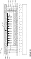
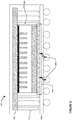
- the ASIC package 101 includes an ASIC die 103 including a silicon substrate 131 and one or more metal layers 133.
- the ASIC die 103 may be positioned such that the metal layer is adjacent to a packaging substrate 109.
- An integrated voltage regulator die 105 may be mounted to the backside of the ASIC die 103, adjacent to the silicon substrate 131.
- Power may be delivered to the ASIC die 103 by the integrated voltage regulator die 105 using a backside power distribution network PDN 107 including through-silicon vias (TSVs) 171 and a redistribution layer 173.
- the ASIC package 201 may include a housing, such as housing 140 in which at least some of the components of the ASIC package 101 may be positioned.
- increases in processing speed of an ASIC die may increase the amount of power required to operate the ASIC die.
- An increase in power drawn by an ASIC die within a typical ASIC package may result in an increase of heat within the ASIC package due to copper losses generated by the wires and/or other such connections which carry the power through the ASIC package. Copper losses, also known as "I 2 R losses", where 'I' is the current flowing through the copper wiring and 'R' is the resistance of the wiring, is the amount of heat dissipated as current passes through wiring.
- the increase in temperature generated by the increased power draw of the ASIC die may result in solder electromigration and potential failure of solder joints.
- the increase of temperature may also affect the thermal performance of the ASIC die and other components within the ASIC package, potentially leading to failure of the ASIC die, failure of other components of the ASIC package, or reduced processing performance.
- a voltage regulator may be integrated into the ASIC package
- the packaging substrate 109 may be configured to connect the ASIC package 101 to a circuit board or other such chip carrier.
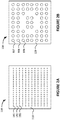
- the packaging substrate 109 may have arrays of connectors on its top side and bottom side, as shown in FIGURES 2A and 2B , respectively. In some instances, connectors may be included on the sides of the packaging substrate 109. Referring to FIGURE 1 , although the packaging substrate 109 is shown as being outside of housing 140, the packaging substrate 109 may be positioned fully or partially within the housing 140.
- a top side 119 of the packaging substrate 109 shows a plurality of connectors, including connectors 191-193.
- the connectors, including connectors 191-193, may be connector pads onto which other components of the ASIC package 101 may be connected, as described herein.
- the connector pads may be gold, nickel, tin, copper, solder, or other such conductive materials.
- the top side 119 of the packaging substrate 109 may include any number of connector pads arranged in any layout.
- the arrangement and number of connectors, including connector pads 191-193, shown in FIGURE 2A is merely for illustration.
- the number and arrangement of connector pads on the top side of the packaging substrate may be based on the design and arrangement of the ASIC die 103, integrated voltage regulator die 105, and/or other components within the ASIC package 101 to allow for the ASIC package to attach to the top side of the packaging substrate 119.
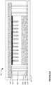
- FIGURE 2B shows a bottom side 129 of the packaging substrate including a plurality of connectors, including connectors 197-199. For clarity, only a portion of the connectors on the bottom side 129 are labeled.
- the connectors, including connectors 197-199 may be configured to connect or otherwise mount the ASIC package 101 to a printed circuit board (PCB), socket, or other such chip carrier.
- the connectors may be solder balls, pins, sockets, etc.
- the connectors 197-199 may be gold, nickel, tin, copper, solder, or other such conductive material.
- the bottom side 129 of the packaging substrate may include any number of connectors in any arrangement.
- the arrangement and number of connectors, including connectors 197-199, shown in FIGURE 2B is merely for illustration.
- the connectors on the bottom side 129 of the packaging substrate may be solder balls arranged in a ball grid array (BGA).
- BGA ball grid array
- Other such arrangements and connectors may include contacts arranged in a land grid array (LGA), connector pins arranged in a pin grid array (PGA), etc.
- the integrated voltage regulator die 105 may be connected to one or more connector pads on the top side 119 packaging substrate 109.
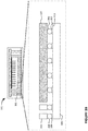
- the connection between the voltage regulator die 105 and the packaging substrate 109 may be made via one or more through mold vias (TMVs), such as TMV 305, as shown in FIGURE 3A .
- TMVs through mold vias
- FIGURE 3A For clarity, only a portion of the TMVs shown in FIGURE 3A are labeled.
- Each TMV may connect the integrated voltage regulator die 105 to the packaging substrate 109 via a connector pad or other such connector.
- the first end 315 of TMV 305 may be attached to a connector pad 399 and the opposite end 325 of the TMV 305 may be attached to the integrated voltage regulator die 105.
- connection between the TMVs and the connector pads may be made via a soldered flip chip bump.
- FIGURE 3B shows an exploded side-view of a portion 301 of the ASIC package 101, including the connection between TMV 305 and connector pad 399.
- the first end 315 of the TMV 305 is connected to connector pad 399 on the top side 119 of the packaging substrate 109 via a soldered flip chip bump 398.
- the TMVs are shown as being connected via soldered flip chip bumps in FIGURE 3B , other connectors and connections may be used.
- the metal layer 133 of the ASIC die 103 may also be connected to the packaging substrate 109.
- the connection of the metal layer 133 to the packaging substrate 109 may be made via flip chip bumps and connector pads, or other such connectors.
- flip chip bump 396 connects the metal layer 133 to connector pad 397, on the top side 119 of the packaging substrate.
- the flip chip bumps are shown in FIGURE 3B as being soldered onto connector pads, such as flip chip bump 396 being soldered onto connector pad 397, other connections may be used.
- Power may be supplied to the ASIC package 101 by an external power source.
- the external power source may provide power to the ASIC package 101 through the chip carrier to which the ASIC package 101 is mounted.
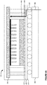
- power shown as arrow 490, may be supplied from an external power source (not shown) to the PCB 409.
- PCB 409 may supply the power to a connector on the packaging substrate.
- the packaging substrate may include a redistribution layer etched onto, or otherwise embedded within, that routes power between the connectors on the bottom side 129 of the packaging substrate and connector pads 119 on the top side of the packaging substrate 109.
- a redistribution layer etched onto, or otherwise embedded within, that routes power between the connectors on the bottom side 129 of the packaging substrate and connector pads 119 on the top side of the packaging substrate 109.
- power 490 delivered by the PCB, or other such chip mount, at connector 492 on the bottom side 129 of the packaging substrate 109 may be routed by the redistribution layer to connector pad 494 on the top side 119 of the packaging substrate.
- FIGURE 4A illustrates the power 490 being supplied to connector 492 and routed to connector pad 494, power may be supplied to any of the connectors on the bottom side of the packaging substrate 109, and in some instances, to more than one connectors.
- the power may be routed by the redistribution layer from the one or more connectors to one or more of the connector pads. For instance, power may be routed from one or more of the connectors on the bottom side 129 of the packaging substrate 109 to one, two, three, or more connector pads on the top side 119 of the packaging substrate 109.
- Power may be carried from the packaging substrate 109 to the integrated voltage regulator die 105 by one or more TMVs.
- FIGURE 4A shows power 490 being routed by TMV 405 from connector pad 494 to the integrated voltage regulator die 105.
- power is shown being routed through only TMV 405. In some instances, power may be routed to the integrated voltage regulator die 105 by more than one TMV.
- Power received by the integrated voltage regulator die may be considered the input power supply.
- the input power supply may be delivered to the integrated voltage regulator die 105 at a higher voltage level and lower current level than the input power supply delivered directly to the ASIC die.
- the integrated voltage regulator die 105 may provide power to the ASIC die 103 with a different supply voltage level.
- the integrated voltage regulator die 105 may operate as a switching voltage regulator and adjust the amount of voltage supplied to the ASIC die based on the needs of the ASIC die or other components within the ASIC package 101.
- the integrated voltage regulator die 105 may deliver power to the ASIC die 107 via backside TSVs.
- power illustrated by arrow 480 may be provided from the integrated voltage regulator die 105 to a backside redistribution layer 173.
- the redistribution layer 173 may direct power to one or more TSV 470, including TSV 171, embedded within the silicon layer 131 of the ASIC die 107.
- FIGURE 4B illustrates power being delivered to all of the TSVs 470, power may be delivered to any number of TSVs.
- the backside redistribution layer 173 may be etched into and/or positioned above the silicon layer 131.
- the backside redistribution layer 173 together with the TSVs may be used to create inductors for use by the integrated voltage regulator die 105.
- Deep trench capacitors (DTCs) may also be embedded into the silicon layer 131 of the ASIC die 107 for use by the integrated voltage regulator die 105.
- switching voltage regulators typically require many inductors and capacitors to operate.
- the backside redistribution layer 173, the TSVs 470, as well as the DTC's embedded silicon may provide at least some the functionality of inductors and capacitors.
- the inductors and DTCs may be stacked onto the ASIC die.
- increases in processing speed of an ASIC die may increase the amount of power required to operate the ASIC die.
- An increase in power drawn by an ASIC die within an ASIC package without an integrated voltage regulator die may result in an increase of heat within the ASIC package due to copper losses generated by the wires and/or other such connections which carry the power through the ASIC package.
- the integrated voltage regulator die 105 may cap the amount of power drawn by the components within ASIC package 101, such as ASIC die 107.
- the integrated voltage regulator die 105 may include a closed loop feedback system to provide a steady voltage output.
- the integrated voltage regulator die 105 may throttle the amount of power drawn, such as when the temperature of the ASIC die 107 is above a particular value or the ASIC die 107 does not require full power to operate.
- the integrated voltage regulator die 105 may also accept higher input voltages, thereby reducing the current supplied to the ASIC package 101 by an external power supply. Accordingly, the amount of current carried by the wires, traces, and/or other such connections on or within the ASIC package may be reduced, resulting in a decrease in the amount of copper losses and minimizing electromigration failure risk in the ASIC package.
- the integrated voltage regulator die 105 may reduce overall power consumption and increase power efficiency of the ASIC package 101.
- the voltage regulator may maintain a consistent power draw from the external power source, thereby preventing or reducing the number of increases in power carried by the wires, traces, and/or other such connections on or within the ASIC package 101.
- the integrated voltage regulator die 105 can include a closed loop feedback system to minimize voltage fluctuations output.
- a feedback sense line may monitor the voltage output by the integrated voltage regulator die 105 and feed monitored voltage level back to the integrated voltage regulator die 105.
- the feedback sense line may have high bandwidth, so the integrated voltage regulator die 105 may be able to compensate for voltage fluctuations quickly. By doing such, inductive noise caused by voltage fluctuations may be reduced.
- FIGURE 5 illustrates an interior and exterior collection of connectors, 595 and 590, respectively, on the top side 519 of a packaging substrate 509.
- power may be delivered by the connectors within the interior 595 of the packaging substrate 509 and data may be delivered by the connections within the exterior 590 of the packaging substrate 509.
- the data connections between the ASIC die 607 and the packaging substrate 609 may be moved to the interior collection of connectors 695. Accordingly, the distance data needs to travel from the ASIC die 607 to the packaging substrate 609 may be reduced, as illustrated by arrows 696, resulting in improved communication speeds and reduced signal loss.
- the data connections may be routed by the redistribution layer in the packaging substrate and may include SERDES connections, parallel connections, serial connections, etc.
- each ASIC package may include any number of ASIC dies.
- each ASIC package may include any number of voltage regulators or other components.
- the packages described herein are described as ASIC packages having ASIC dies, any type of die may be used, such as a memory die or integrated circuit die.
- the features described herein allow for the integration of an integrated voltage regulator die into the ASIC package. By doing such, the copper losses generated by wires, traces, and/or other such connections which carry the power through the ASIC package to the ASIC die may be reduced. Moreover, by positioning the integrated voltage regulator die above the ASIC die, the distance data communications travel between the ASIC die and the PCB may be reduced.
Landscapes
- Semiconductor Integrated Circuits (AREA)
- Engineering & Computer Science (AREA)
- Power Engineering (AREA)
- Internal Circuitry In Semiconductor Integrated Circuit Devices (AREA)
Priority Applications (1)
| Application Number | Priority Date | Filing Date | Title |
|---|---|---|---|
| EP24204293.5A EP4468351A3 (fr) | 2020-02-12 | 2020-11-05 | Régulateur de tension intégré côté arrière pour circuits intégrés |
Applications Claiming Priority (1)
| Application Number | Priority Date | Filing Date | Title |
|---|---|---|---|
| US16/788,994 US11276668B2 (en) | 2020-02-12 | 2020-02-12 | Backside integrated voltage regulator for integrated circuits |
Related Child Applications (1)
| Application Number | Title | Priority Date | Filing Date |
|---|---|---|---|
| EP24204293.5A Division EP4468351A3 (fr) | 2020-02-12 | 2020-11-05 | Régulateur de tension intégré côté arrière pour circuits intégrés |
Publications (2)
| Publication Number | Publication Date |
|---|---|
| EP3866193A1 true EP3866193A1 (fr) | 2021-08-18 |
| EP3866193B1 EP3866193B1 (fr) | 2024-10-09 |
Family
ID=73288366
Family Applications (2)
| Application Number | Title | Priority Date | Filing Date |
|---|---|---|---|
| EP24204293.5A Pending EP4468351A3 (fr) | 2020-02-12 | 2020-11-05 | Régulateur de tension intégré côté arrière pour circuits intégrés |
| EP20205957.2A Active EP3866193B1 (fr) | 2020-02-12 | 2020-11-05 | Régulateur de tension intégré de côté arrière pour circuits intégrés |
Family Applications Before (1)
| Application Number | Title | Priority Date | Filing Date |
|---|---|---|---|
| EP24204293.5A Pending EP4468351A3 (fr) | 2020-02-12 | 2020-11-05 | Régulateur de tension intégré côté arrière pour circuits intégrés |
Country Status (6)
| Country | Link |
|---|---|
| US (5) | US11276668B2 (fr) |
| EP (2) | EP4468351A3 (fr) |
| CN (2) | CN112185919B (fr) |
| DK (1) | DK3866193T3 (fr) |
| FI (1) | FI3866193T3 (fr) |
| TW (2) | TWI846585B (fr) |
Families Citing this family (6)
| Publication number | Priority date | Publication date | Assignee | Title |
|---|---|---|---|---|
| US11444059B2 (en) * | 2019-12-19 | 2022-09-13 | Micron Technology, Inc. | Wafer-level stacked die structures and associated systems and methods |
| US11844199B2 (en) | 2022-01-26 | 2023-12-12 | Advanced Semiconductor Engineering, Inc. | Electronic device |
| US12213247B2 (en) | 2022-07-14 | 2025-01-28 | Advanced Semiconductor Engineering, Inc. | Electronic device |
| US12550785B2 (en) * | 2022-08-24 | 2026-02-10 | International Business Machines Corporation | Separated input/output (I/O) and shared power terminals for a carrier wafer with a built-in device for bonding with another device wafer |
| CN117747592A (zh) * | 2022-09-15 | 2024-03-22 | 辉达公司 | 用于gpu芯片和片上系统设备封装的反向嵌入式电源结构 |
| US20240186248A1 (en) * | 2022-12-01 | 2024-06-06 | Adeia Semiconductor Bonding Technologies Inc. | Backside power delivery network |
Citations (4)
| Publication number | Priority date | Publication date | Assignee | Title |
|---|---|---|---|---|
| US20120012990A1 (en) * | 2010-07-16 | 2012-01-19 | Stats Chippac, Ltd. | Semiconductor Device and Method of Forming Protective Layer Over Exposed Surfaces of Semiconductor Die |
| US20120032340A1 (en) * | 2010-08-06 | 2012-02-09 | Stats Chippac, Ltd. | Semiconductor Die and Method of Forming FO-WLCSP Vertical Interconnect Using TSV and TMV |
| US20120061814A1 (en) * | 2010-09-14 | 2012-03-15 | Stats Chippac, Ltd. | Semiconductor Device and Method of Forming Leadframe Interposer Over Semiconductor Die and TSV Substrate for Vertical Electrical Interconnect |
| WO2019133019A1 (fr) * | 2017-12-30 | 2019-07-04 | Intel Corporation | Architecture de puce de silicium empilée avec une puce retournée mixte et une interconnexion de connexion de fils |
Family Cites Families (44)
| Publication number | Priority date | Publication date | Assignee | Title |
|---|---|---|---|---|
| KR100891269B1 (ko) * | 2001-01-31 | 2009-04-06 | 소니 가부시끼 가이샤 | 반도체 장치 및 그 제조 방법 |
| US6894266B2 (en) | 2003-02-14 | 2005-05-17 | Oplink Communications, Inc. | Single chip ASIC and compact packaging solution for an avalanche photodiode (APD) and bias circuit |
| US7166740B2 (en) * | 2003-07-14 | 2007-01-23 | Schering Ag | Process for the production of triiodotrimesic acid |
| US7091586B2 (en) | 2003-11-04 | 2006-08-15 | Intel Corporation | Detachable on package voltage regulation module |
| US7668415B2 (en) * | 2004-09-27 | 2010-02-23 | Qualcomm Mems Technologies, Inc. | Method and device for providing electronic circuitry on a backplate |
| US7098070B2 (en) | 2004-11-16 | 2006-08-29 | International Business Machines Corporation | Device and method for fabricating double-sided SOI wafer scale package with through via connections |
| JP2008015336A (ja) | 2006-07-07 | 2008-01-24 | Fujitsu Ltd | 回路基板及び半導体デバイスの光結合方法 |
| WO2008036726A2 (fr) | 2006-09-19 | 2008-03-27 | Ibiden Co., Ltd. | Dispositif d'interconnexion optique et procédé de production de ce dernier |
| US7692278B2 (en) * | 2006-12-20 | 2010-04-06 | Intel Corporation | Stacked-die packages with silicon vias and surface activated bonding |
| US8265432B2 (en) | 2008-03-10 | 2012-09-11 | International Business Machines Corporation | Optical transceiver module with optical windows |
| US8168939B2 (en) | 2008-07-09 | 2012-05-01 | Luxtera, Inc. | Method and system for a light source assembly supporting direct coupling to an integrated circuit |
| WO2013109889A2 (fr) | 2012-01-18 | 2013-07-25 | The Trustees Of Columbia University In The City Of New York | Systèmes et procédés associés à des régulateurs de tension intégrés |
| US9129935B1 (en) | 2012-10-05 | 2015-09-08 | Altera Corporation | Multi-chip packages with reduced power distribution network noise |
| US9297971B2 (en) | 2013-04-26 | 2016-03-29 | Oracle International Corporation | Hybrid-integrated photonic chip package with an interposer |
| WO2015047330A1 (fr) * | 2013-09-27 | 2015-04-02 | Intel Corporation | Conditionnement de puce à substrat superposeur pour composants passifs |
| US20150187608A1 (en) * | 2013-12-26 | 2015-07-02 | Sanka Ganesan | Die package architecture with embedded die and simplified redistribution layer |
| US9406648B2 (en) | 2014-09-25 | 2016-08-02 | Taiwan Semiconductor Manufacturing Company, Ltd. | Power supply arrangement for semiconductor device |
| KR101793967B1 (ko) | 2014-12-24 | 2017-11-06 | 인텔 코포레이션 | 적층형 집적 회로 패키지에서의 통합형 수동 구성요소 장치 및 이를 포함한 컴퓨팅 디바이스 |
| US10236209B2 (en) * | 2014-12-24 | 2019-03-19 | Intel Corporation | Passive components in vias in a stacked integrated circuit package |
| US20160314003A1 (en) | 2015-04-23 | 2016-10-27 | PhotonIC International Pte. Ltd. | Photonics-Optimized Processor System |
| EP3430646B1 (fr) * | 2016-03-16 | 2021-11-10 | INTEL Corporation | Interposeurs en marche d'escalier à blindage intégré pour boîtier électroniques |
| US10096582B2 (en) * | 2016-07-08 | 2018-10-09 | Cisco Technology, Inc. | Enhanced power distribution to application specific integrated circuits (ASICS) |
| US20180052281A1 (en) | 2016-08-16 | 2018-02-22 | Advanced Semiconductor Engineering, Inc. | Substrate, semiconductor device and semiconductor package structure |
| WO2018127531A1 (fr) | 2017-01-06 | 2018-07-12 | Rockley Photonics Limited | Conditionnement combiné d'asic et de photonique au silicium |
| CN106980159B (zh) | 2017-03-07 | 2019-01-22 | 中国科学院微电子研究所 | 基于光电混合集成的光电模块封装结构 |
| GB2561974B (en) | 2017-03-23 | 2022-05-04 | Rockley Photonics Ltd | Leaf switch module and optoelectronic switch |
| WO2018190952A1 (fr) | 2017-04-14 | 2018-10-18 | Google Llc | Intégration d'un circuit intégré photonique sur silicium pour débit de données élevé |
| US10727198B2 (en) * | 2017-06-30 | 2020-07-28 | Taiwan Semiconductor Manufacturing Co., Ltd. | Semiconductor package and method manufacturing the same |
| US11239377B2 (en) | 2017-08-07 | 2022-02-01 | Rockley Photonics Limited | Optoelectronic module package |
| SG11202001724TA (en) | 2017-09-06 | 2020-03-30 | Agency Science Tech & Res | Photonic integrated circuit package and method of forming the same |
| US10725254B2 (en) | 2017-09-20 | 2020-07-28 | Aayuna Inc. | High density opto-electronic interconnection configuration utilizing passive alignment |
| WO2019066937A1 (fr) | 2017-09-29 | 2019-04-04 | Intel Corporation | Configuration de boîtier de puce haute densité sur des cartes système |
| US10505509B2 (en) | 2017-10-31 | 2019-12-10 | Cisco Technology, Inc. | Process and temperature insensitive linear circuit |
| WO2019132958A1 (fr) | 2017-12-29 | 2019-07-04 | Intel Corporation | Ensembles microélectroniques |
| DE102018205156A1 (de) * | 2018-04-05 | 2019-10-10 | Robert Bosch Gmbh | MEMS-Element und ASIC-Element |
| FR3080218B1 (fr) | 2018-04-11 | 2022-02-11 | St Microelectronics Grenoble 2 | Dispositif electronique comprenant des puces electroniques |
| US10560765B2 (en) | 2018-04-25 | 2020-02-11 | Western Digital Technologies, Inc. | Node with combined optical and electrical switching |
| US10529677B2 (en) * | 2018-04-27 | 2020-01-07 | Advanced Micro Devices, Inc. | Method and apparatus for power delivery to a die stack via a heat spreader |
| US10811404B2 (en) * | 2018-05-31 | 2020-10-20 | Taiwan Semiconductor Manufacturing Company, Ltd. | Package structure and method of manufacturing the same |
| US11462463B2 (en) * | 2018-09-27 | 2022-10-04 | Intel Corporation | Microelectronic assemblies having an integrated voltage regulator chiplet |
| US11024617B2 (en) | 2018-10-26 | 2021-06-01 | Micron Technology, Inc. | Semiconductor packages having photon integrated circuit (PIC) chips |
| US10928585B2 (en) | 2018-10-26 | 2021-02-23 | Micron Technology, Inc. | Semiconductor devices having electro-optical substrates |
| US11424953B2 (en) | 2018-11-28 | 2022-08-23 | Kinnexa, Inc. | Modular physical layer and integrated connector module for local area networks |
| US20200203470A1 (en) | 2018-12-20 | 2020-06-25 | Intel Corporation | Magnetic mold material inductors for electronic packages |
-
2020
- 2020-02-12 US US16/788,994 patent/US11276668B2/en active Active
- 2020-09-30 CN CN202011056882.5A patent/CN112185919B/zh active Active
- 2020-09-30 CN CN202411451686.6A patent/CN119480824A/zh active Pending
- 2020-10-15 TW TW112133768A patent/TWI846585B/zh active
- 2020-10-15 TW TW109135652A patent/TWI817049B/zh active
- 2020-11-05 FI FIEP20205957.2T patent/FI3866193T3/fi active
- 2020-11-05 EP EP24204293.5A patent/EP4468351A3/fr active Pending
- 2020-11-05 DK DK20205957.2T patent/DK3866193T3/da active
- 2020-11-05 EP EP20205957.2A patent/EP3866193B1/fr active Active
-
2022
- 2022-02-08 US US17/667,104 patent/US11830855B2/en active Active
-
2023
- 2023-08-29 US US18/239,368 patent/US12394756B2/en active Active
-
2024
- 2024-09-03 US US18/823,093 patent/US12278217B2/en active Active
-
2025
- 2025-07-23 US US19/278,168 patent/US20250349802A1/en active Pending
Patent Citations (4)
| Publication number | Priority date | Publication date | Assignee | Title |
|---|---|---|---|---|
| US20120012990A1 (en) * | 2010-07-16 | 2012-01-19 | Stats Chippac, Ltd. | Semiconductor Device and Method of Forming Protective Layer Over Exposed Surfaces of Semiconductor Die |
| US20120032340A1 (en) * | 2010-08-06 | 2012-02-09 | Stats Chippac, Ltd. | Semiconductor Die and Method of Forming FO-WLCSP Vertical Interconnect Using TSV and TMV |
| US20120061814A1 (en) * | 2010-09-14 | 2012-03-15 | Stats Chippac, Ltd. | Semiconductor Device and Method of Forming Leadframe Interposer Over Semiconductor Die and TSV Substrate for Vertical Electrical Interconnect |
| WO2019133019A1 (fr) * | 2017-12-30 | 2019-07-04 | Intel Corporation | Architecture de puce de silicium empilée avec une puce retournée mixte et une interconnexion de connexion de fils |
Also Published As
| Publication number | Publication date |
|---|---|
| US20250006706A1 (en) | 2025-01-02 |
| TW202131420A (zh) | 2021-08-16 |
| US12394756B2 (en) | 2025-08-19 |
| EP3866193B1 (fr) | 2024-10-09 |
| TWI817049B (zh) | 2023-10-01 |
| US20250349802A1 (en) | 2025-11-13 |
| US20210249384A1 (en) | 2021-08-12 |
| EP4468351A3 (fr) | 2025-03-26 |
| US11830855B2 (en) | 2023-11-28 |
| TWI846585B (zh) | 2024-06-21 |
| CN112185919B (zh) | 2024-10-29 |
| EP4468351A2 (fr) | 2024-11-27 |
| CN119480824A (zh) | 2025-02-18 |
| US12278217B2 (en) | 2025-04-15 |
| CN112185919A (zh) | 2021-01-05 |
| DK3866193T3 (da) | 2025-01-06 |
| US11276668B2 (en) | 2022-03-15 |
| TW202401594A (zh) | 2024-01-01 |
| US20230402430A1 (en) | 2023-12-14 |
| US20220157787A1 (en) | 2022-05-19 |
| FI3866193T3 (fi) | 2024-12-12 |
Similar Documents
| Publication | Publication Date | Title |
|---|---|---|
| US12278217B2 (en) | Backside integrated voltage regulator for integrated circuits | |
| US12051679B2 (en) | Backside interconnection interface die for integrated circuits package | |
| US11830804B2 (en) | Over and under interconnects | |
| US6979891B2 (en) | Integrated circuit packaging architecture | |
| US11322435B2 (en) | Package substrate having power trace pattern and ground trace pattern, and semiconductor package including the same | |
| CN116169109A (zh) | 电子封装 | |
| HK40043995A (en) | Backside integrated voltage regulator for integrated circuits | |
| HK40121705A (zh) | 用於集成电路的背侧集成电压调节器 | |
| US12213247B2 (en) | Electronic device | |
| HK40043995B (zh) | 用於集成电路的背侧集成电压调节器 | |
| CN116544206A (zh) | 一种具有分离式基板的晶圆级集成结构 | |
| US20230130354A1 (en) | Three-dimensional semiconductor package having a stacked passive device | |
| WO2022198675A1 (fr) | Module multi-puce et dispositif électronique comportant un module multi-puce | |
| CN222394818U (zh) | 电子器件 | |
| KR102686915B1 (ko) | 멀티 패스 파워 플립 칩 패키지 | |
| US20240357751A1 (en) | Electronic device | |
| US20250006585A1 (en) | Semiconductor packages with multiple types of conductive components | |
| EP4553898A2 (fr) | Circuit intégré tridimensionnel comprenant une cellule de commutation | |
| Chen et al. | An overview of electrical and mechanical aspects of electronic packaging | |
| KR20250071143A (ko) | 스위치 셀을 포함하는 3차원 집적 회로 | |
| CN116759402A (zh) | 半导体器件 | |
| CN121666150A (zh) | 半导体封装和半导体封装组装 | |
| CN121619928A (zh) | 集成电压调节模块的封装结构及其制备方法 | |
| CN119725316A (zh) | 芯片封装结构及电子设备 |
Legal Events
| Date | Code | Title | Description |
|---|---|---|---|
| PUAI | Public reference made under article 153(3) epc to a published international application that has entered the european phase |
Free format text: ORIGINAL CODE: 0009012 |
|
| STAA | Information on the status of an ep patent application or granted ep patent |
Free format text: STATUS: THE APPLICATION HAS BEEN PUBLISHED |
|
| AK | Designated contracting states |
Kind code of ref document: A1 Designated state(s): AL AT BE BG CH CY CZ DE DK EE ES FI FR GB GR HR HU IE IS IT LI LT LU LV MC MK MT NL NO PL PT RO RS SE SI SK SM TR |
|
| STAA | Information on the status of an ep patent application or granted ep patent |
Free format text: STATUS: REQUEST FOR EXAMINATION WAS MADE |
|
| 17P | Request for examination filed |
Effective date: 20220217 |
|
| RBV | Designated contracting states (corrected) |
Designated state(s): AL AT BE BG CH CY CZ DE DK EE ES FI FR GB GR HR HU IE IS IT LI LT LU LV MC MK MT NL NO PL PT RO RS SE SI SK SM TR |
|
| STAA | Information on the status of an ep patent application or granted ep patent |
Free format text: STATUS: EXAMINATION IS IN PROGRESS |
|
| 17Q | First examination report despatched |
Effective date: 20230727 |
|
| REG | Reference to a national code |
Ref country code: DE Ref legal event code: R079 Free format text: PREVIOUS MAIN CLASS: H01L0023485000 Ipc: H01L0025160000 Ref country code: DE Ref legal event code: R079 Ref document number: 602020038962 Country of ref document: DE Free format text: PREVIOUS MAIN CLASS: H01L0023485000 Ipc: H01L0025160000 |
|
| GRAJ | Information related to disapproval of communication of intention to grant by the applicant or resumption of examination proceedings by the epo deleted |
Free format text: ORIGINAL CODE: EPIDOSDIGR1 |
|
| STAA | Information on the status of an ep patent application or granted ep patent |
Free format text: STATUS: GRANT OF PATENT IS INTENDED |
|
| GRAP | Despatch of communication of intention to grant a patent |
Free format text: ORIGINAL CODE: EPIDOSNIGR1 |
|
| RIC1 | Information provided on ipc code assigned before grant |
Ipc: H01L 25/18 20060101ALI20240409BHEP Ipc: H01L 25/065 20060101ALI20240409BHEP Ipc: H01L 23/00 20060101ALI20240409BHEP Ipc: H01L 23/498 20060101ALI20240409BHEP Ipc: H01L 25/16 20060101AFI20240409BHEP |
|
| INTG | Intention to grant announced |
Effective date: 20240426 |
|
| GRAS | Grant fee paid |
Free format text: ORIGINAL CODE: EPIDOSNIGR3 |
|
| GRAA | (expected) grant |
Free format text: ORIGINAL CODE: 0009210 |
|
| STAA | Information on the status of an ep patent application or granted ep patent |
Free format text: STATUS: THE PATENT HAS BEEN GRANTED |
|
| AK | Designated contracting states |
Kind code of ref document: B1 Designated state(s): AL AT BE BG CH CY CZ DE DK EE ES FI FR GB GR HR HU IE IS IT LI LT LU LV MC MK MT NL NO PL PT RO RS SE SI SK SM TR |
|
| REG | Reference to a national code |
Ref country code: CH Ref legal event code: EP |
|
| P01 | Opt-out of the competence of the unified patent court (upc) registered |
Free format text: CASE NUMBER: APP_52180/2024 Effective date: 20240917 |
|
| REG | Reference to a national code |
Ref country code: DE Ref legal event code: R096 Ref document number: 602020038962 Country of ref document: DE |
|
| REG | Reference to a national code |
Ref country code: IE Ref legal event code: FG4D |
|
| REG | Reference to a national code |
Ref country code: FI Ref legal event code: FGE |
|
| REG | Reference to a national code |
Ref country code: DK Ref legal event code: T3 Effective date: 20250103 |
|
| REG | Reference to a national code |
Ref country code: NL Ref legal event code: FP |
|
| REG | Reference to a national code |
Ref country code: LT Ref legal event code: MG9D |
|
| REG | Reference to a national code |
Ref country code: SE Ref legal event code: TRGR |
|
| REG | Reference to a national code |
Ref country code: AT Ref legal event code: MK05 Ref document number: 1731561 Country of ref document: AT Kind code of ref document: T Effective date: 20241009 |
|
| PG25 | Lapsed in a contracting state [announced via postgrant information from national office to epo] |
Ref country code: PT Free format text: LAPSE BECAUSE OF FAILURE TO SUBMIT A TRANSLATION OF THE DESCRIPTION OR TO PAY THE FEE WITHIN THE PRESCRIBED TIME-LIMIT Effective date: 20250210 Ref country code: HR Free format text: LAPSE BECAUSE OF FAILURE TO SUBMIT A TRANSLATION OF THE DESCRIPTION OR TO PAY THE FEE WITHIN THE PRESCRIBED TIME-LIMIT Effective date: 20241009 Ref country code: IS Free format text: LAPSE BECAUSE OF FAILURE TO SUBMIT A TRANSLATION OF THE DESCRIPTION OR TO PAY THE FEE WITHIN THE PRESCRIBED TIME-LIMIT Effective date: 20250209 |
|
| PG25 | Lapsed in a contracting state [announced via postgrant information from national office to epo] |
Ref country code: BG Free format text: LAPSE BECAUSE OF FAILURE TO SUBMIT A TRANSLATION OF THE DESCRIPTION OR TO PAY THE FEE WITHIN THE PRESCRIBED TIME-LIMIT Effective date: 20241009 |
|
| PG25 | Lapsed in a contracting state [announced via postgrant information from national office to epo] |
Ref country code: ES Free format text: LAPSE BECAUSE OF FAILURE TO SUBMIT A TRANSLATION OF THE DESCRIPTION OR TO PAY THE FEE WITHIN THE PRESCRIBED TIME-LIMIT Effective date: 20241009 |
|
| PG25 | Lapsed in a contracting state [announced via postgrant information from national office to epo] |
Ref country code: NO Free format text: LAPSE BECAUSE OF FAILURE TO SUBMIT A TRANSLATION OF THE DESCRIPTION OR TO PAY THE FEE WITHIN THE PRESCRIBED TIME-LIMIT Effective date: 20250109 |
|
| PG25 | Lapsed in a contracting state [announced via postgrant information from national office to epo] |
Ref country code: LV Free format text: LAPSE BECAUSE OF FAILURE TO SUBMIT A TRANSLATION OF THE DESCRIPTION OR TO PAY THE FEE WITHIN THE PRESCRIBED TIME-LIMIT Effective date: 20241009 Ref country code: GR Free format text: LAPSE BECAUSE OF FAILURE TO SUBMIT A TRANSLATION OF THE DESCRIPTION OR TO PAY THE FEE WITHIN THE PRESCRIBED TIME-LIMIT Effective date: 20250110 Ref country code: AT Free format text: LAPSE BECAUSE OF FAILURE TO SUBMIT A TRANSLATION OF THE DESCRIPTION OR TO PAY THE FEE WITHIN THE PRESCRIBED TIME-LIMIT Effective date: 20241009 |
|
| PG25 | Lapsed in a contracting state [announced via postgrant information from national office to epo] |
Ref country code: PL Free format text: LAPSE BECAUSE OF FAILURE TO SUBMIT A TRANSLATION OF THE DESCRIPTION OR TO PAY THE FEE WITHIN THE PRESCRIBED TIME-LIMIT Effective date: 20241009 |
|
| PG25 | Lapsed in a contracting state [announced via postgrant information from national office to epo] |
Ref country code: RS Free format text: LAPSE BECAUSE OF FAILURE TO SUBMIT A TRANSLATION OF THE DESCRIPTION OR TO PAY THE FEE WITHIN THE PRESCRIBED TIME-LIMIT Effective date: 20250109 |
|
| PG25 | Lapsed in a contracting state [announced via postgrant information from national office to epo] |
Ref country code: SM Free format text: LAPSE BECAUSE OF FAILURE TO SUBMIT A TRANSLATION OF THE DESCRIPTION OR TO PAY THE FEE WITHIN THE PRESCRIBED TIME-LIMIT Effective date: 20241009 |
|
| PG25 | Lapsed in a contracting state [announced via postgrant information from national office to epo] |
Ref country code: MC Free format text: LAPSE BECAUSE OF FAILURE TO SUBMIT A TRANSLATION OF THE DESCRIPTION OR TO PAY THE FEE WITHIN THE PRESCRIBED TIME-LIMIT Effective date: 20241009 |
|
| REG | Reference to a national code |
Ref country code: DE Ref legal event code: R097 Ref document number: 602020038962 Country of ref document: DE |
|
| PG25 | Lapsed in a contracting state [announced via postgrant information from national office to epo] |
Ref country code: LU Free format text: LAPSE BECAUSE OF NON-PAYMENT OF DUE FEES Effective date: 20241105 |
|
| PG25 | Lapsed in a contracting state [announced via postgrant information from national office to epo] |
Ref country code: EE Free format text: LAPSE BECAUSE OF FAILURE TO SUBMIT A TRANSLATION OF THE DESCRIPTION OR TO PAY THE FEE WITHIN THE PRESCRIBED TIME-LIMIT Effective date: 20241009 |
|
| PG25 | Lapsed in a contracting state [announced via postgrant information from national office to epo] |
Ref country code: RO Free format text: LAPSE BECAUSE OF FAILURE TO SUBMIT A TRANSLATION OF THE DESCRIPTION OR TO PAY THE FEE WITHIN THE PRESCRIBED TIME-LIMIT Effective date: 20241009 |
|
| PG25 | Lapsed in a contracting state [announced via postgrant information from national office to epo] |
Ref country code: SK Free format text: LAPSE BECAUSE OF FAILURE TO SUBMIT A TRANSLATION OF THE DESCRIPTION OR TO PAY THE FEE WITHIN THE PRESCRIBED TIME-LIMIT Effective date: 20241009 |
|
| PG25 | Lapsed in a contracting state [announced via postgrant information from national office to epo] |
Ref country code: CZ Free format text: LAPSE BECAUSE OF FAILURE TO SUBMIT A TRANSLATION OF THE DESCRIPTION OR TO PAY THE FEE WITHIN THE PRESCRIBED TIME-LIMIT Effective date: 20241009 |
|
| PG25 | Lapsed in a contracting state [announced via postgrant information from national office to epo] |
Ref country code: IT Free format text: LAPSE BECAUSE OF FAILURE TO SUBMIT A TRANSLATION OF THE DESCRIPTION OR TO PAY THE FEE WITHIN THE PRESCRIBED TIME-LIMIT Effective date: 20241009 |
|
| PLBE | No opposition filed within time limit |
Free format text: ORIGINAL CODE: 0009261 |
|
| STAA | Information on the status of an ep patent application or granted ep patent |
Free format text: STATUS: NO OPPOSITION FILED WITHIN TIME LIMIT |
|
| 26N | No opposition filed |
Effective date: 20250710 |
|
| REG | Reference to a national code |
Ref country code: DE Ref legal event code: R079 Ref document number: 602020038962 Country of ref document: DE Free format text: PREVIOUS MAIN CLASS: H01L0025160000 Ipc: H10W0090000000 |
|
| REG | Reference to a national code |
Ref country code: CH Ref legal event code: U11 Free format text: ST27 STATUS EVENT CODE: U-0-0-U10-U11 (AS PROVIDED BY THE NATIONAL OFFICE) Effective date: 20251201 |
|
| PGFP | Annual fee paid to national office [announced via postgrant information from national office to epo] |
Ref country code: NL Payment date: 20251126 Year of fee payment: 6 |
|
| PGFP | Annual fee paid to national office [announced via postgrant information from national office to epo] |
Ref country code: DE Payment date: 20251128 Year of fee payment: 6 |
|
| PGFP | Annual fee paid to national office [announced via postgrant information from national office to epo] |
Ref country code: GB Payment date: 20251127 Year of fee payment: 6 |
|
| PGFP | Annual fee paid to national office [announced via postgrant information from national office to epo] |
Ref country code: FI Payment date: 20251125 Year of fee payment: 6 Ref country code: DK Payment date: 20251125 Year of fee payment: 6 |
|
| PGFP | Annual fee paid to national office [announced via postgrant information from national office to epo] |
Ref country code: FR Payment date: 20251125 Year of fee payment: 6 |
|
| PGFP | Annual fee paid to national office [announced via postgrant information from national office to epo] |
Ref country code: BE Payment date: 20251127 Year of fee payment: 6 |
|
| PGFP | Annual fee paid to national office [announced via postgrant information from national office to epo] |
Ref country code: CH Payment date: 20251201 Year of fee payment: 6 Ref country code: SE Payment date: 20251127 Year of fee payment: 6 |
|
| PGFP | Annual fee paid to national office [announced via postgrant information from national office to epo] |
Ref country code: IE Payment date: 20251127 Year of fee payment: 6 |
|
| PG25 | Lapsed in a contracting state [announced via postgrant information from national office to epo] |
Ref country code: HU Free format text: LAPSE BECAUSE OF FAILURE TO SUBMIT A TRANSLATION OF THE DESCRIPTION OR TO PAY THE FEE WITHIN THE PRESCRIBED TIME-LIMIT; INVALID AB INITIO Effective date: 20201105 |
|
| PG25 | Lapsed in a contracting state [announced via postgrant information from national office to epo] |
Ref country code: CY Free format text: LAPSE BECAUSE OF FAILURE TO SUBMIT A TRANSLATION OF THE DESCRIPTION OR TO PAY THE FEE WITHIN THE PRESCRIBED TIME-LIMIT; INVALID AB INITIO Effective date: 20201105 |