EP3867977B1 - Gemeinsam genutztes mmwellen- und sub-6-ghz-antennensystem - Google Patents
Gemeinsam genutztes mmwellen- und sub-6-ghz-antennensystem Download PDFInfo
- Publication number
- EP3867977B1 EP3867977B1 EP19895609.6A EP19895609A EP3867977B1 EP 3867977 B1 EP3867977 B1 EP 3867977B1 EP 19895609 A EP19895609 A EP 19895609A EP 3867977 B1 EP3867977 B1 EP 3867977B1
- Authority
- EP
- European Patent Office
- Prior art keywords
- antenna
- electronic device
- array
- antenna system
- patch
- Prior art date
- Legal status (The legal status is an assumption and is not a legal conclusion. Google has not performed a legal analysis and makes no representation as to the accuracy of the status listed.)
- Active
Links
Images


Classifications
-
- H—ELECTRICITY
- H01—ELECTRIC ELEMENTS
- H01Q—ANTENNAS, i.e. RADIO AERIALS
- H01Q1/00—Details of, or arrangements associated with, antennas
- H01Q1/12—Supports; Mounting means
- H01Q1/22—Supports; Mounting means by structural association with other equipment or articles
- H01Q1/2283—Supports; Mounting means by structural association with other equipment or articles mounted in or on the surface of a semiconductor substrate as a chip-type antenna or integrated with other components into an IC package
-
- H—ELECTRICITY
- H01—ELECTRIC ELEMENTS
- H01Q—ANTENNAS, i.e. RADIO AERIALS
- H01Q1/00—Details of, or arrangements associated with, antennas
- H01Q1/12—Supports; Mounting means
- H01Q1/22—Supports; Mounting means by structural association with other equipment or articles
- H01Q1/24—Supports; Mounting means by structural association with other equipment or articles with receiving set
- H01Q1/241—Supports; Mounting means by structural association with other equipment or articles with receiving set used in mobile communications, e.g. GSM
- H01Q1/242—Supports; Mounting means by structural association with other equipment or articles with receiving set used in mobile communications, e.g. GSM specially adapted for hand-held use
- H01Q1/243—Supports; Mounting means by structural association with other equipment or articles with receiving set used in mobile communications, e.g. GSM specially adapted for hand-held use with built-in antennas
-
- H—ELECTRICITY
- H01—ELECTRIC ELEMENTS
- H01Q—ANTENNAS, i.e. RADIO AERIALS
- H01Q21/00—Antenna arrays or systems
- H01Q21/28—Combinations of substantially independent non-interacting antenna units or systems
-
- H—ELECTRICITY
- H01—ELECTRIC ELEMENTS
- H01Q—ANTENNAS, i.e. RADIO AERIALS
- H01Q25/00—Antennas or antenna systems providing at least two radiating patterns
-
- H—ELECTRICITY
- H01—ELECTRIC ELEMENTS
- H01Q—ANTENNAS, i.e. RADIO AERIALS
- H01Q5/00—Arrangements for simultaneous operation of antennas on two or more different wavebands, e.g. dual-band or multi-band arrangements
- H01Q5/30—Arrangements for providing operation on different wavebands
- H01Q5/307—Individual or coupled radiating elements, each element being fed in an unspecified way
- H01Q5/342—Individual or coupled radiating elements, each element being fed in an unspecified way for different propagation modes
- H01Q5/35—Individual or coupled radiating elements, each element being fed in an unspecified way for different propagation modes using two or more simultaneously fed points
-
- H—ELECTRICITY
- H01—ELECTRIC ELEMENTS
- H01Q—ANTENNAS, i.e. RADIO AERIALS
- H01Q5/00—Arrangements for simultaneous operation of antennas on two or more different wavebands, e.g. dual-band or multi-band arrangements
- H01Q5/40—Imbricated or interleaved structures; Combined or electromagnetically coupled arrangements, e.g. comprising two or more non-connected fed radiating elements
-
- H—ELECTRICITY
- H01—ELECTRIC ELEMENTS
- H01Q—ANTENNAS, i.e. RADIO AERIALS
- H01Q9/00—Electrically-short antennas having dimensions not more than twice the operating wavelength and consisting of conductive active radiating elements
- H01Q9/04—Resonant antennas
- H01Q9/0407—Substantially flat resonant element parallel to ground plane, e.g. patch antenna
-
- H—ELECTRICITY
- H01—ELECTRIC ELEMENTS
- H01Q—ANTENNAS, i.e. RADIO AERIALS
- H01Q9/00—Electrically-short antennas having dimensions not more than twice the operating wavelength and consisting of conductive active radiating elements
- H01Q9/04—Resonant antennas
- H01Q9/30—Resonant antennas with feed to end of elongated active element, e.g. unipole
- H01Q9/42—Resonant antennas with feed to end of elongated active element, e.g. unipole with folded element, the folded parts being spaced apart a small fraction of the operating wavelength
Definitions
- the present disclosure relates generally to an electronic device, and, in particular embodiments, to a system and method for an arrangement of antennas in an electronic device.
- Mobile devices are equipped with an assortment of antennas, each designed to provide access to a different radio access technology (RAT).
- RAT radio access technology
- a mobile device may have different antennas to support third generation (3G), fourth generation (4G), Long-Term Evolution (LTE), and/or fifth generation (5G) New Radio (NR) wireless communications, and to access Wi-Fi, Bluetooth, near field communication (NFC), and / or global positioning satellite (GPS) signals.
- 3G third generation
- 4G fourth generation
- LTE Long-Term Evolution
- NR New Radio
- Wi-Fi Wireless Fidelity
- NFC near field communication
- GPS global positioning satellite
- United States patent application US 2018/0233817 A1 discloses an antenna module, a first antenna and a second ground conductor operating as a ground electrode of the first antenna as well as a second antenna.
- United States patent application US 2017/0214120 A1 discloses an electronic device including a circuit board and radiators. The electronic device is provided with a first feeding signal to transmit or receive a wireless signal in a first frequency band and an additional feeding signal to transmit or receive a wireless signal in various frequency bands that are lower than the first frequency band.
- inventive aspects are described primarily in the context of an antenna system operating over sub-6 gigahertz (GHz) and millimeter wave (mmWave) frequencies, it should also be appreciated that these inventive aspects may also be applicable to other antennas operating over other frequency spectrums, which can also take advantage of the inventive concepts disclosed herein.
- inventive aspects may also be applicable to other antennas operating over other frequency spectrums, which can also take advantage of the inventive concepts disclosed herein.
- the various embodiments presented in this disclosure are described primarily in the context of an antenna system on a mobile device, the resulting antenna system may provide wireless communication in a base station that can benefit from antenna placement and antenna arrangement compactness.
- 5G Fifth generation
- 5G NR New Radio
- 5G NR provides for an increased bandwidth, higher data rates, and higher system capacity than in currently available communication technologies.
- a common deployment strategy for the transition from LTE to 5G NR is the addition of 5G NR base stations (i.e., gNB or gNodeB) to existing Long-Term Evolution (LTE) wireless communication networks, which provide a wide coverage layer to the network operators.
- 5G NR base stations i.e., gNB or gNodeB
- LTE Long-Term Evolution
- mobile devices are equipped with a variety of antennas to provide operational capabilities within 2G/3G/4G/LTE/5G NR. This is in addition to other antennas that may provide support for, for example, data or power transference (e.g., global positioning satellite (GPS), Wi-Fi, Bluetooth, and near field communications (NFC), etc.).
- GPS global positioning satellite
- Wi-Fi Wireless Fidelity
- NFC near field communications
- Embodiments of this disclosure provide structures and methods for arrangement and design of compact antenna systems capable of operating over multiple radio access technologies (RATs).
- RATs radio access technologies
- an antenna system and a method of operation and assembly are provided.
- the antenna system includes a sub-6 GHz antenna and a millimeter wave (mmWave) antenna, supporting sub-6 GHz and mmWave frequency spectrums, respectively.
- the feed network for the mmWave antenna is embedded within a transmission line medium, which concurrently provides a signal return path for the sub-6 GHz antenna and, optionally for the mmWave antenna, to a ground plane. This arrangement allows for a more compact design and an improvement in component placement volumetric efficiency within the host device.
- the transmission line medium may be, for example, a stripline or a microstrip.
- the sub-6 GHz antenna may be an inverted-F antenna (IFA), a loop antenna, a slot antenna, or any other antenna type having a signal return path to a ground plane.
- An example of the mmWave antenna may be a dual-polarized patch array antenna.
- the mmWave antenna may support both horizontal and vertical polarizations with main beams pointing away from the mobile device and in the same direction.
- grounded via structures within the transmission line medium may provide for an improved isolation between the mmWave antenna signal and the sub-6 GHz antenna signal.
- the sub-6 GHz antenna may include a plurality of openings or cavities.
- the mmWave antenna may include an array of antenna elements configured to radiate at mmWave carrier frequencies, and each antenna element in the array of antenna elements may radiate through a different one of the plurality of openings, or cavities, of the sub-6 GHz antenna.
- the mmWave antenna may be a patch antenna located above the sub-6 GHz antenna, where a radiator of the sub-6 GHz antenna is a ground plane of the mmWave antenna.
- the mmWave antenna includes an array of antenna elements, a flex circuit, a circuit clip (c-clip), printed circuit boards (PCBs) connected to via c-clips, and an integrated circuit (IC).
- the PCB may be a flex a circuit board.
- the mmWave antenna can be arranged within a metal frame of the mobile device.
- the sub-6 GHz antenna can include a dielectric cover facing the outside portion of the mobile device and an internal metal frame or a metal on top of a dielectric carrier facing the interior portion of the mobile device.
- the integrated circuit is located on an opposing side to the array of antenna elements.
- the mmWave antenna is connected to a PCB of the mobile device through a board-to-board connector and the flex circuit.
- the flex circuit can electrically connect the IC to the main PCB housing a processor and a modem.
- the mmWave antenna can include a first (e.g., 1x4 patch array) and a second (e.g., 2x2 patch array) array of patch antennas.
- Each patch antenna of the first array may radiate through a respective opening of a metal frame of the electronic device located perpendicular to a display side of the electronic device, providing coverage for the side of the phone.
- Each patch antenna of the second array may radiate through a dielectric back cover of the electronic device located opposite the display side of the electronic device, providing coverage for the back of the phone.
- the mmWave antenna can include a single polarized dipole array. Each element in the single polarized dipole array may radiate between the metal frame and the display side of the electronic device, providing coverage for the front of the phone.
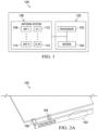
- Figure 1 illustrates an embodiment electronic device 100 capable of operating over multiple radio access technologies (RATs).
- the electronic device 100 may be any user-side device configured to access a network, such as a cellular device, a tablet, a personal computer, a mobile station (STA), a smartwatch, a vehicle, or any other wirelessly enabled user-side device.
- the user-device may provide wireless access to a base station, a global positioning satellite (GPS), a user equipment (UE), an inductive power source, or the like.
- GPS global positioning satellite
- UE user equipment
- inductive power source or the like.
- the electronic device 100 may be any network-side device configured to provide wireless access to a network, such as an enhanced Node B (eNodeB or eNB), a gNB, a transmit/receive point (TRP), a macro-cell, a femtocell, a Wi-Fi Access Point (AP), and other wirelessly enabled devices.
- Base stations may provide wireless access in accordance with one or more wireless communication protocols, e.g., 5th generation new radio (5G NR), LTE, LTE advanced (LTE-A), High Speed Message Access (HSPA), Wi-Fi 802.11a/b/g/n/ac, etc.
- the electronic device 100 may include various other wireless devices, such as modems, sensors, graphics processors, etc.
- the electronic device 100 includes a processor 102, a modem 104, and an antenna system 106, which may (or may not) be arranged as shown.
- the processor 102 may be any component or collection of components adapted to perform computations and/or other processing related tasks
- the modem 104 may be any component or collection of components adapted to generate communication signals for execution by the processor 102.
- the processor 102 and the modem 104 may be housed within a main printed circuit board (PCB) 120.
- PCB main printed circuit board
- the electronic device 100 is shown to have a single processor. However, in some embodiments multiple processors may be included in the electronic device 100. In some embodiments, the electronic device 100 may include different types of processing units, such as a graphics processing unit (GPU), a digital signal processor (DSP), etc.
- GPU graphics processing unit
- DSP digital signal processor
- the UE 100 may include additional components not depicted in Figure 1 , such as a non-transitory computer readable medium, long-term storage (e.g., non-volatile memory, etc.) or a phase locked loop.
- the antenna system 106 includes N number of antennas, antenna 1 108 to antenna N 110. Each antenna is capable of accessing a same or a different network, satellite, or device. The antenna is used to radiate or to receive signals, and able to operate across a variety of frequency spectrums.
- the antenna system 106 also includes M number of integrated circuits (ICs), IC 1 112 to IC M 114.
- the ICs connect the various components of the host device to one another, to amplify a signal, to filter out signals, etc.
- each antenna e.g., Ant 1 108 to Ant N 110
- an integrated circuit may connect multiple antennas to the processor 102 and modem 104.
- some antennas may share a common integrated circuit for connection to the processor 102 and / or modem 104.
- Embodiments of this disclosure provide a space saving structure that allows a transmission line medium used for a signal return path of one antenna to be used as a feed network for a second antenna.
- the signal return path for the first antenna may also be the signal return path for the second antenna.
- the ground structure of the transmission line medium additionally isolates the signal of the second antenna from the signal of the first antenna.
- a mmWave antenna be it an antenna on board (AoB) type or antenna in package (AiP) type, generally has no electrical direct current (DC) connection with a sub-6 GHz antenna.
- the mmWave antenna exists separately from the sub-6 GHz antenna, each radiating separately without sharing any common components.
- embodiments of this disclosure provide a mmWave antenna that all or portions of the antenna may connect with all or portions of the sub-6 GHz antenna.
- the connection between the two antennas may be a high impedance line, or lines, that may be used as ports of the sub-6 GHz antenna.
- the mmWave antenna implementation in, for example a 5G system can coexist with a sub-6 GHz radio within a shared volume.
- Figures 2A-C illustrate multi-angular views of an embodiment antenna system 150 that includes a compact arrangement of shared components in a first antenna and a second antenna.
- Figure 2A illustrates a top angular view of the embodiment antenna system 150
- Figure 2B illustrates an enlarged front-side of the embodiment antenna system 150
- Figure 2C illustrates an enlarged back-side view of the embodiment antenna system 150.
- the first antenna of the antenna system 150 is capable of operating over the sub-6 GHz frequency spectrum.
- the second antenna of the antenna system 150 is capable of operating over the mmWave frequency spectrum.
- the first antenna may be any type of antenna having a signal return path to a ground plane and capable of operating over the sub-6 GHz frequency spectrum.
- the first antenna includes a radiating element 152, a feed network 154, and a signal return path 156.
- the ground plane for the sub-6 GHz antenna is electrically connected to a common ground of the antenna system 150 through the signal return path 156.
- the signal return path 156 may be a stripline transmission line that includes a strip of conductive metal sandwiched between two parallel ground plates and insulated by a dielectric material.
- the parallel ground plates provide a signal return path for both the first and the second antenna.
- the conductive metal provides the feed path for the second antenna.
- via structures may connect the parallel ground plates of the transmission line medium to each other, creating a walled plane on the sides of the conductive metal. The parallel ground plates and the walled via structure provide isolation for the feed path of the second antenna from outside signals that may interfere with signal distribution.
- the first antenna may be an inverted-F antenna (IFA) capable of operating over the sub-6 GHz (i.e., below 6 GHz) frequency spectrum.
- the inverted-F antenna may be used in a planar implementation for wireless circuitry in the form of a planar inverted-F antenna (PIFA), a printed inverted-F antenna, a meandered printed inverted-F antenna, a patch antenna, a shorted patch antenna, or the like.
- the inverted-F antenna may be constructed within, for example, a microstrip electromagnetic transmission line medium.
- the antenna element is wide with the ground plane located underneath.
- the sub-6 GHz antenna may be a loop antenna, a slot antenna, or any other type of antenna used to support operational functionality in the below 6 GHz frequency spectrum.
- the second antenna may be any type of antenna having a feed network implemented in a conductive component of a transmission line that also includes a ground plane providing a signal return path for the sub-6 GHz antenna.
- the second antenna includes a radiating element 158, a signal trace 160, and a signal return path 162.
- the signal return path 156 of the first antenna may be the signal return path 162 of the second antenna.
- the second antenna is a 1x4 dual polarized patch array antenna capable of operating over the millimeter wave frequency spectrum (i.e., between 30 GHz and 300 GHz).
- the number of patch array elements and the arrangement (row and / or column) of the elements are non-limiting, and other arrangements of varying quantities may be contemplated.
- the illustration of the second antenna being a dual polarized patch array antenna is a non-limiting example and, in other embodiments, the second antenna may be a single polarized patch array antenna, a dipole antenna, a monopole antenna, an aperture antenna, or the like.
- the radiator of the sub-6 GHz antenna may use the metal frame 164 around the mobile phone and the sub-6 GHz antenna may include a plurality of openings 166 or cavities.
- the mmWave antenna may include an array of antenna elements configured to radiate at mmWave carrier frequencies, and each antenna element in the array of antenna elements may radiate through a different one of the plurality of openings 166 or cavities of the sub-6 GHz antenna. It is also contemplated that in some other embodiments, two or more antenna elements may share and radiate through a same opening or cavity of the sub-6 GHz antenna.
- each patch antenna array element may face an opening of the sub-6 GHz antenna radiator and radiate through the openings.
- the metal portion in-between the openings may improve isolation between the patch array elements.
- the mmWave antenna may be a patch antenna located above the sub-6 GHz antenna, where a radiator of the sub-6 GHz antenna is a ground plane of the mmWave antenna.
- Figures 3A-B illustrate gain patterns in a horizontal and a vertical polarization corresponding to the second antenna of the embodiment antenna system 150.
- Figure 3A is a realized horizontal gain pattern of the second antenna operating over the millimeter-wave frequency spectrum.
- Figure 3B is a realized vertical gain pattern of the second antenna operating over the millimeter wave frequency spectrum.
- the realized gain patterns shown in Figures 3A-B illustrate the realized gain pattern of the embodiment 1x4 dual polarized patch antenna radiating through the openings of the exterior frame of a host device.
- the mmWave antenna supports both horizontal and vertical polarizations.
- the main beams point away from the mobile device, and in the same direction.
- first antenna and the second antenna, of the antenna system 150 are isolated from each other at greater than 30 dB up to, at least, 35 GHz and at some frequencies at greater than 40 dB. This isolation is greater in the vertical polarization, where it is consistently greater than 40 dB up to, at least, 35 GHz.
- the system efficiency of the first antenna may be greater than -8 dBp. In particular, at frequencies between 0.8 GHz and 1.6 GHz, the system efficiency is greater than -4 dBp.
- the return loss of the first antenna may be less than 14 dB. In particular, at frequencies between 1 and 1.8 GHz, the return loss of the first antenna may be between 2 and 8 dB, depending on the particular frequency.
- Figures 4A-D illustrate multi-angular views of an embodiment antenna system 200.
- Figure 4A illustrates an angular front-side view of the embodiment antenna 200.
- Figure 4B illustrates an angular front-side view of the embodiment antenna system 200 placed within a metal frame of a mobile device.
- the metal frame of the mobile device may act as the ground plane of the sub-6 GHz antenna.
- the antenna system 200 includes a patch array antenna 202 operating over the mmWave frequency spectrum.
- the antenna system 200 also includes a second antenna 204 configured to operate over the sub-6 GHz frequency spectrum.
- the patch array antenna 202 is shown to have four elements arranged in a single row (i.e., 1x4 patch array antenna).
- the patch array antenna 202 may include different number of elements, which may be arranged in different configurations. Therefore, it should be understood that the number of elements in the patch array antenna 202 is non-limiting, and may have varying number of elements that may be arranged in a variety of configurations.
- the patch array antenna 202 radiates through an opening 220 of the mobile device, for example, an opening 220 on the side metal frame 222 as shown in Figure 4B .
- the patch array antenna 202 provides side coverage perpendicular to the side of, and away from, the mobile device.
- the metal frame 222 may act as a ground structure for the second antenna 204, which may also be shared as a ground structure for the first patch array antenna 202.
- the second antenna 204 may have openings allowing for the patch array antenna 202 to radiate through.
- the patch array antenna 202 may be located on top of the second antenna 204.
- the patch array antenna 202 uses the radiator of the second antenna 204 as a ground plane.
- the second antenna 204 may be a device with a dielectric cover on the outside and an internal metal frame. In other embodiments, the second antenna 204 may be a device with a dielectric cover on the outside and a metal on top of dielectric carrier as the antenna.
- FIG. 4C illustrates an angular backside view of the embodiment antenna 200.
- an integrated circuit (IC) 206 is located on the backside of the patch array antenna 202.
- the IC 206 is connected to the patch array antenna 202 through the metal frame structure and to the main board 208 of the mobile device.
- the main board 208 may be a printed circuit board (PCB) that may include the processor 102, the modem 104, and a board-to-board connector 210.
- the board-to-board connector may be any type of interface that allows for an electrical connection access to and / or from the components of the main board 208.
- the IC 206 may be connected to the board-to-board connector 210 using a connector 212.
- the circuit 212 may be a flex circuit.
- Figure 4D illustrates an angular backside view of the embodiment antenna 200 with an alternative arrangement of components and electrical connections than the embodiment shown in Figure 4C .
- an integrated circuit (IC) 226 is located on a sub-board 228.
- the sub-board 228 may be a printed circuit board.
- the sub-board 228 may be a flex circuit board.
- the sub-board 228 is connected to the main board using a circuit clip (c-clip) 230.
- the sub-board 228 may is connected to the patch array antenna 202 using a connector 232 in the form of a flex circuit.
- Figures 5A-B illustrate multi-angular views of an embodiment antenna system 250.
- Figure 5A illustrates an angular topside view of the antenna system 250.
- Figure 5B illustrates an angular side-view of the antenna system 250.
- the antenna system 250 includes a first patch array antenna 252 and a second patch array antenna 254, each operating over the mmWave frequency spectrum.
- the antenna system 250 also includes a third antenna 256 configured to operate over the sub-6 GHz frequency spectrum.
- the first patch array antenna 252 is shown to have four elements arranged in a single row (i.e., 1x4 patch array antenna).
- the second patch array antenna 254 is shown to have four elements. However, the four elements are arranged in two columns and two rows (i.e., 2x2 patch array antenna).
- the 1x4 patch array antenna 252 radiates through an opening of a mobile device, for example, an opening on the side metal frame.
- the 1x4 patch array antenna 252 provides coverage at the side of the phone.
- the patch array antenna 254 may be positioned on the backside of the mobile device.
- the backside of the mobile device may be a dielectric structure (i.e., back cover).
- the patch array antenna 254 provides backside reception coverage for the mobile device.
- the patch array antennas 252 and 254 may each include different number of elements and may be arranged in different configurations.
- the first patch array antenna 252 may have eight elements arranged in a single row (i.e., 1x8 patch array antenna).
- the first patch array antenna 252 may have six elements arranged in two rows (i.e., 2x3 patch array antenna).
- the second patch array antenna 254 may have 8 elements arranged in two columns and four rows (i.e., 2x4 patch array antenna).
- the second patch array antenna 254 may have 16 elements arranged in four columns and four rows (i.e., 4x4 patch array antenna). Therefore, it should be understood that the number of elements in each patch array antenna 252 and 254 is non-limiting and each may have varying number of elements in a variety of configurations.
- Figures 6A-C illustrate multi-angular views of an embodiment antenna system 300.
- the antenna system 300 includes three different patch array antennas providing a three sided reception and transmission coverage for a host device.
- Figure 6A illustrates an angular top-side view of the antenna system 300.
- Figure 6B illustrates an angular side-view of the antenna system 300.
- Figure 6C illustrates an angular bottom-side view of the antenna system 300.
- the antenna system 300 includes a first patch array antenna 302, a second patch array antenna 304, and a third patch array antenna 306.
- Each patch array antenna is configured to operate over the mmWave frequency spectrum.
- the antenna system 300 also includes a fourth antenna 308 configured to operate over the sub-6 GHz frequency spectrum.
- the first patch array antenna 302 and the third patch array antenna 306 are shown to have four elements arranged in a single row (i.e., 1x4 patch array antenna).
- the second patch array antenna 304 is shown to have four elements. However, the four elements in the second patch array antenna 304 are arranged in two columns and two rows (i.e., 2x2 patch array antenna).
- the first patch array antenna 302 is shown as a 1x4 dual-polarized patch array antenna.
- the second patch array antenna 304 is shown as a 2x2 dual-polarized patch array antenna.
- the third patch array antenna 306 is shown as a 1x4 single-polarized patch array antenna.
- the first patch array antenna 302 may be placed on a side of a host device, providing a coverage area in the direction perpendicular to the side structure and away from the internal components of the host device.
- the structure of the host device may include openings in a metal frame in which the elements of the first patch array antenna 302 may be able to radiate.
- the metal side frame may be a ground plane for the fourth antenna 308 and the first patch array antenna 302.
- the second patch array antenna 304 may be placed on the backside of the host device, providing a coverage area in the direction perpendicular to the backside and away from the internal components of the host device.
- the backside of the host device may include a dielectric back cover (i.e., non-metal) that allows for the elements of the second patch array antenna 304 to radiate outwards without being reflected back to the device.
- the backside cover may additionally provide protection from damage without having the second patch array antenna 304 being directly exposed to natural elements.
- the third patch array antenna 306 may be placed on the opposite plane to the second patch array antenna 304. In such an arrangement, the third patch array antenna 306 may be able to radiate between the metal frame and the display of the host device. The third patch array antenna 306 may then provide a coverage area in the direction perpendicular to the front-side of the and away from the internal components of the host device.
- the patch array antennas 302, 304, and 306 may each include different number of elements and may be arranged in different configurations. Therefore, it should be understood that the number of elements in each patch array antenna 302, 304, and 306 is non-limiting, and each antenna may have varying number of elements that are arranged in a variety of configurations.
- Figures 7A-7B illustrate an embodiment host device 350.
- Figure 7A is a front side view of the host device 350 and Figure 7B is a backside view of the host device 350.
- the host device 350 may be a cellular phone, a tablet device, or the like capable of operating over multiple RATs.
- the host device 350 includes a housing 352.
- the housing 352 includes an front surface 352a, an back surface 352b, and side surfaces 352c.
- the front surface 352a includes a display region 354.
- the back surface 352b may be a removable or non-removable back cover made of a dielectric material.
- the housing of the electronic device 100 is generally composed of a conductive metal (e.g., aluminum, magnesium, etc.), plastic (polycarbonates, etc.), glass (e.g., aluminosilicate glass, etc.), and/or other materials (e.g., composites) that provide similar rigidity, strength and/or durability.
- a conductive metal e.g., aluminum, magnesium, etc.
- plastic polycarbonates, etc.
- glass e.g., aluminosilicate glass, etc.
- other materials e.g., composites
- parts of the metal in the panels may be used as an external antenna.
- the panels may be made of metal and have plastic or glass openings or be made of plastic or glass to allow for reception or transmission of an internal antenna.
- the host device 350 may host one or more of the antennas previously disclosed in this disclosure.
- the antennas 202 and 204 of Figures 4A-D may be located at the side portions 352c and radiate outwardly and away from the host device 350.
- the antenna 252 in Figures 5A-5B may be located at the side portions 352c and the antenna 254 may be located at the back surface 352b.
- the antennas 252 and 254 radiate outwardly and away from the host device 350.
- the antenna 302 in Figures 6A-6C may be located at the side portions 352c, the antenna 304 may be located at the back surface 352b, and the antenna 306 may be located at the front surface 352a. In this example, the antennas 302, 304, and 306 radiate outwardly and away from the host device 350.
- each antenna is strategically placed to reduce the signal interference with respect to the signal radiating from other antennas of the device.
- One effective method to improve isolation is by physically separating the antennas from each other.
- Another method to improve isolation is by placing the antennas such that the polarization of the antennas are orthogonal to each other.
- antennas may be arranged at a horizontal and/or vertical offset in relation to each other, as the signal coupling is generally reduced as a function of its distance.
- antennas may be placed perpendicular to each other to create different polarizations.
- a wireless device may have a primary cellular antenna, a diversity cellular antenna, a global positioning satellite (GPS) antenna, a WiFi antenna, and a near field communication (NFC) antenna.
- Other antennas may be included to achieve specific communication goals. Alternatively, some antennas may be omitted, for example, to reduce the size, complexity and/or cost of the wireless device.
- a wireless device may have one or more of each type of antenna. Some non-cellular antennas may be for receivers, such as in a GPS antenna, while other non-cellular antennas, such as in the WiFi antenna, may be for a transmitter and a receiver.
- the primary cellular antenna is the primary communication antenna and is responsible for the transmission and reception of analog and digital signals.
- the location of the primary cellular antenna is at the lower vertical position of the cellular device. This is typically done to reduce the specific absorption rate (SAR) and increase the total radiated power (TRP) by moving the bulk of the antenna away from the human head.
- SAR specific absorption rate
- TRP total radiated power
- the primary cellular antenna may typically be of a planar inverted-F antenna (PIFA), a folded inverted-F antenna, a monopole antenna, a loop antenna, microstrip patch antenna, a folded inverted conformal antenna type, or a modified version of any one of the foregoing or other type of antennas.
- PIFA planar inverted-F antenna
- a folded inverted-F antenna a monopole antenna, a loop antenna, microstrip patch antenna, a folded inverted conformal antenna type, or a modified version of any one of the foregoing or other type of antennas.
- many different types of antennas may be used to support the various regulatory and system requirements specific to different carriers.
- secondary cellular antennas or diversity antennas are added as an alternative to the primary cellular antenna.
- the secondary cellular antenna or the diversity antenna is for receiving only (or for receiving and transmitting when transmit diversity is supported).
- the receiving device may receive more than one copy of the original signal due to the multipath propagation, as a result of signal reflection and dispersion.
- the secondary cellular antenna may be a same antenna type as the primary cellular antenna.
- the secondary cellular antenna may be a different type of antenna that operates at a same frequency as the primary cellular antenna.
- the wireless data modem selects the strongest signal from the various signal copies received at the multiplicity of antennas.
- the wireless data modem may combine the received signals to increase the received signal power level and the signal to noise ratio (SNR) of the received signal by combining and weighing the signals from the different paths.
- SNR signal to noise ratio
- multiple methods can be used to increase signal reliability.
- MIMO multiple-input and multiple-output
- a simple wireless communication system is usually of a single-input and single-output (SISO) type.
- SISO single-input and single-output
- a single antenna may be used as a transmitter and a single antenna may be used as the receiver.
- MIMO is a smart antenna technology that uses a multiplicity of antennas to take advantage of multipath propagation to send and receive signals simultaneously over the same radio channel.
- MIMO technology can be of the diversity type to improve the reliability of the signal or of the spatial-multiplexing type which increases data throughput.
- Other MIMO type techniques are available that improve both the reliability and data throughput.
- MIMO relies on a plurality of antennas to improve wireless communication performance.
- MIMO technology may have two or more antennas at each of the transmit or receive ends of the communication paths.
- a 2x2 MIMO is a configuration where two antennas are at the transmit end and two antennas are arranged in the receive end.
- a 4x4 MIMO is a configuration where four antennas are at the transmit end and four antennas are at the receive end.
- an 8x8 MIMO is a configuration with eight antennas at each of the transmit and receive ends. In general, the greater the number of antennas, the greater the bandwidth capacity, data speed transfer, and signal reliability.
- the physical proximity of the primary and diversity antennas in a wireless device may contribute to correlation of received signal from different antennas, and as a result reduce diversity gain and MIMO throughput.
- the diversity antenna is arranged at the upper vertical position of the cellular device to maximize the distance between it and the primary antenna.
- an antenna arrangement is disclosed that increases isolation and reduces correlation between the primary and secondary antennas in a device with an extended display.
- a ground plane slot structure separates the two ground plane regions to improve isolation and reduce correlation between antennas.
- FIG. 8 is a diagram of a network 800 for communicating data.
- the network 800 includes a base station 810 having a coverage area 801, a plurality of UEs 820, and a backhaul network 830.
- the base station 810 establishes uplink (dashed line) and/or downlink (dotted line) connections with the UEs 820, which serve to carry data from the UEs 820 to the base station 810 and vice-versa.
- Data communicated over the uplink/downlink connections may include data communicated between the UEs 820, as well as data communicated to/from a remote-end (not shown) by way of the backhaul network 830.
- the term "base station” refers to any network-side device configured to provide wireless access to a network, such as an enhanced Node B (eNodeB or eNB), a gNB, a transmit/receive point (TRP), a macro-cell, a femtocell, a Wi-Fi Access Point (AP), and other wirelessly enabled devices.
- Base stations may provide wireless access in accordance with one or more wireless communication protocols, e.g., 5th generation new radio (5G NR), LTE, LTE advanced (LTE-A), High Speed Message Access (HSPA), Wi-Fi 802.11a/b/g/n/ac, etc.
- 5G NR 5th generation new radio
- LTE LTE advanced
- HSPA High Speed Message Access
- Wi-Fi 802.11a/b/g/n/ac etc.
- the term "UE” refers to any user-side device configured to access a network by establishing a wireless connection with a base station, such as a mobile device, a mobile station (STA), a vehicle, and other wirelessly enabled devices.
- a base station such as a mobile device, a mobile station (STA), a vehicle, and other wirelessly enabled devices.
- the network 800 may include various other wireless devices, such as relays, low power nodes, etc. While it is understood that communication systems may employ multiple access nodes capable of communicating with a number of UEs, only one base station 810, and two UEs 820 are illustrated for simplicity.
- Figure 9 illustrates a block diagram of another embodiment processing system 900 for performing methods described herein, which may be installed in a host device.
- the processing system 900 includes a processor 902, a memory 904, and interfaces 906, 908, 910 which may (or may not) be arranged as shown in Figure 9 .
- the processor 902 may be any component or collection of components adapted to perform computations and/or other processing related tasks
- the memory 904 may be any component or collection of components adapted to store programming and/or instructions for execution by the processor 902.
- the memory 904 includes a non-transitory computer readable medium.
- the interfaces 906, 908, 910 may be any component or collection of components that allow the processing system 900 to communicate with other devices/components and/or a user.
- one or more of the interfaces 906, 908, 910 may be adapted to communicate data, control, or management messages from the processor 902 to applications installed on the host device and/or a remote device.
- one or more of the interfaces 906, 908, 910 may be adapted to allow a user or user device (e.g., personal computer (PC), etc.) to interact/communicate with the processing system 900.
- the processing system 900 may include additional components not depicted in Figure 9 , such as long-term storage (e.g., non-volatile memory, etc.).
- the processing system 900 is included in a network device that is accessing, or part otherwise of, a telecommunications network.
- the processing system 900 is in a network-side device in a wireless or wireline telecommunications network, such as a base station, a relay station, a scheduler, a controller, a gateway, a router, an applications server, or any other device in the telecommunications network.
- the processing system 900 is in a user-side device accessing a wireless or wireline telecommunications network, such as a mobile station, a user equipment (UE), a personal computer (PC), a tablet, a wearable communications device (e.g., a smartwatch, etc.), a wireless capable vehicle, a wireless capable pedestrian, a wireless capable infrastructure element or any other device adapted to access a telecommunications network.
- a wireless or wireline telecommunications network such as a mobile station, a user equipment (UE), a personal computer (PC), a tablet, a wearable communications device (e.g., a smartwatch, etc.), a wireless capable vehicle, a wireless capable pedestrian, a wireless capable infrastructure element or any other device adapted to access a telecommunications network.
- a wireless or wireline telecommunications network such as a mobile station, a user equipment (UE), a personal computer (PC), a tablet, a wearable communications device (e.g., a smartwatch, etc
- one or more of the interfaces 906, 908, 910 connects the processing system 900 to a transceiver adapted to transmit and receive signaling over the telecommunications network.
- Figure 10 illustrates a block diagram of a transceiver 1000 adapted to transmit and receive signaling over a telecommunications network.
- the transceiver 1000 may be installed in a host device. As shown, the transceiver 1000 comprises a network-side interface 1002, a coupler 1004, a transmitter 1006, a receiver 1008, a signal processor 1010, and a device-side interface 1012.
- the network-side interface 1002 may include any component or collection of components adapted to transmit or receive signaling over a wireless or wireline telecommunications network.
- the coupler 1004 may include any component or collection of components adapted to facilitate bi-directional communication over the network-side interface 1002.
- the transmitter 1006 may include any component or collection of components (e.g., up-converter, power amplifier, etc.) adapted to convert a baseband signal into a modulated carrier signal suitable for transmission over the network-side interface 1002.
- the receiver 1008 may include any component or collection of components (e.g., down-converter, low noise amplifier, etc.) adapted to convert a carrier signal received over the network-side interface 1002 into a baseband signal.
- the signal processor 1010 may include any component or collection of components adapted to convert a baseband signal into a data signal suitable for communication over the device-side interface(s) 1012, or vice-versa.
- the device-side interface(s) 1012 may include any component or collection of components adapted to communicate data-signals between the signal processor 1010 and components within the host device (e.g., the processing system 900, local area network (LAN) ports
- the transceiver 1000 may transmit and receive signaling over any type of communications medium.
- the transceiver 1000 transmits and receives signaling over a wireless medium.
- the transceiver 1000 may be a wireless transceiver adapted to communicate in accordance with a wireless telecommunications protocol, such as a cellular protocol (e.g., long-term evolution (LTE), etc.), a wireless local area network (WLAN) protocol (e.g., Wi-Fi, etc.), or any other type of wireless protocol (e.g., Bluetooth, near field communication (NFC), etc.).
- a wireless telecommunications protocol such as a cellular protocol (e.g., long-term evolution (LTE), etc.), a wireless local area network (WLAN) protocol (e.g., Wi-Fi, etc.), or any other type of wireless protocol (e.g., Bluetooth, near field communication (NFC), etc.).
- the network-side interface 1002 comprises one or more antenna/radiating elements.
- the network-side interface 1002 may include a single antenna, multiple separate antennas, or a multi-antenna array configured for multi-layer communication, e.g., single input multiple output (SIMO), multiple input single output (MISO), multiple input multiple output (MIMO), etc.
- the transceiver 1000 transmits and receives signaling over a wireline medium, e.g., twisted-pair cable, coaxial cable, optical fiber, etc.
- Specific processing systems and/or transceivers may utilize all of the components shown, or only a subset of the components, and levels of integration may vary from device to device.
Landscapes
- Engineering & Computer Science (AREA)
- Physics & Mathematics (AREA)
- Electromagnetism (AREA)
- Computer Networks & Wireless Communication (AREA)
- Microelectronics & Electronic Packaging (AREA)
- Variable-Direction Aerials And Aerial Arrays (AREA)
- Support Of Aerials (AREA)
Claims (13)
- Antennensystem, konfiguriert für den Einsatz in einer elektronischen Vorrichtung (100), wobei das Antennensystem (106; 150; 200) Folgendes umfasst:eine erste Antenne (204), die für den Betrieb bei Frequenzen unter 6 Gigahertz (GHz) konfiguriert ist; undeine zweite Antenne (202), die für den Betrieb bei Millimeterwellenfrequenzen konfiguriert ist, wobei ein Speisenetzwerk der zweiten Antenne (202) in ein Übertragungsleitungsmedium eines Signalrückpfads (156) der ersten Antenne (204) eingebettet ist,wobei die elektronische Vorrichtung (100) eine erste Leiterplatte, PCB, umfasst, die einen Prozessor (102; 902) und ein Modem (104) umfasst,dadurch gekennzeichnet, dassdie zweite Antenne (202) ferner Folgendes umfasst:eine flexible Schaltung (232);eine Schaltungsklammer, C-Klammer (230);eine zweite PCB oder eine flexible Leiterplatte (228), die unter Verwendung der C-Klammer (230) elektrisch mit der ersten PCB verbunden ist; undeine integrierte Schaltung, IC (226), die auf der zweiten PCB oder der flexiblen Leiterplatte (228) montiert ist, wobei die IC (226) so konfiguriert ist, dass sie unter Verwendung der flexiblen Leiterplatte (232) elektrisch mit der zweiten Antenne (202) verbunden wird.
- Antennensystem nach Anspruch 1, wobei das Übertragungsleitungsmedium eine Streifenleitungsübertragungsleitung ist.
- Antennensystem nach einem der Ansprüche 1-2, wobei die erste Antenne (204) eine invertierte F-Antenne, IFA, eine Rahmenantenne oder eine Schlitzantenne ist.
- Antennensystem nach einem der Ansprüche 1-2, wobei der Signalrückpfad (156) der ersten Antenne (204) zu einer Masseebene führt.
- Antennensystem nach einem der Ansprüche 1-4, wobei eine Masseebene der ersten Antenne (204) eine Masseebene der zweiten Antenne (202) ist.
- Antennensystem nach einem der Ansprüche 1-5, wobei die erste Antenne (204) eine Vielzahl von Öffnungen (166) umfasst.
- Antennensystem nach Anspruch 6, wobei ein Strahlungselement (152) der ersten Antenne (204) eine Masseebene der zweiten Antenne (202) ist.
- Antennensystem nach Anspruch 7, wobei die zweite Antenne (202) eine Anordnung von Antennenelementen umfasst, die so konfiguriert sind, dass sie bei Millimeterwellenfrequenzen strahlen, und wobeijedes Antennenelement in der Anordnung aus Antennenelementen durch eine andere der Vielzahl von Öffnungen (166) der ersten Antenne (204) strahlt;mindestens ein Antennenelement in der Anordnung aus Antennenelementen durch eine andere der Vielzahl von Öffnungen (166) der ersten Antenne (204) strahlt; oderdie erste Antenne (204) eine Masseebene jedes Antennenelements in der Anordnung aus Antennenelementen ist.
- Antennensystem nach einem der Ansprüche 1-8, wobei die zweite Antenne (202) eine dual polarisierte Patch-Array-Antenne, eine einfach polarisierte Patch-Array-Antenne, eine Dipolantenne, eine Monopolantenne oder eine Aperturantenne ist.
- Antennensystem nach einem der Ansprüche 1 bis 9, wobei sich die zweite Antenne (202) innerhalb eines Metallrahmens der elektronischen Vorrichtung (100) befindet.
- Antennensystem nach einem der Ansprüche 1 bis 10, wobei die elektronische Vorrichtung (100) Folgendes umfasst:eine Vorderseite (352a), die ein Display (354) umfasst;eine Rückseite (352b), die der Vorderseite (352a) gegenüberliegt und eine hintere Abdeckung umfasst; undeine Seite (352c), die senkrecht zur Vorderseite (352a) und zur Rückseite (352b) steht und die Vorderseite (352a) mit der Rückseite (352b) verbindet,wobei die hintere Abdeckung aus einem dielektrischen Material besteht;und wobei die erste Antenne (204) einen inneren Metallrahmen umfasst, der sich zwischen der hinteren Abdeckung und der Vorderseite (352a) der elektronischen Vorrichtung (100) befindet, oder wobei die erste Antenne (204) ein Metall auf einem dielektrischen Träger umfasst,wobei die erste Antenne (204) so konfiguriert ist, dass sie nach außen und von der Rückseite (352b) der elektronischen Vorrichtung (100) weg strahlt.
- Antennensystem nach einem der Ansprüche 1-7 und 10, wobei die zweite Antenne (202) ferner Folgendes umfasst:eine erste Anordnung von Patchantennen, wobei jede Patchantenne der ersten Anordnung von Patchantennen so konfiguriert ist, dass sie durch eine jeweilige Öffnung (220) eines Metallrahmens (164) der elektronischen Vorrichtung (100) strahlt, wobei die Öffnungen (220) des Metallrahmens (164) senkrecht zu einer Displayseite der elektronischen Vorrichtung (100) angeordnet sind; undeine zweite Anordnung von Patchantennen, wobei jede Patchantenne der zweiten Anordnung von Patchantennen so konfiguriert ist, dass sie durch eine dielektrische hintere Abdeckung der elektronischen Vorrichtung (100) strahlt, wobei sich die dielektrische hintere Abdeckung gegenüber der Displayseite der elektronischen Vorrichtung (100) befindet.
- Antennensystem nach Anspruch 12, wobei die zweite Antenne (202) außerdem ein einzelnes polarisiertes Dipol-Array umfasst, wobei jedes Element in dem einzelnen polarisierten Dipol-Array so konfiguriert ist, dass es zwischen dem Metallrahmen (164) und der Displayseite der elektronischen Vorrichtung (100) strahlt.
Applications Claiming Priority (2)
| Application Number | Priority Date | Filing Date | Title |
|---|---|---|---|
| US201862777555P | 2018-12-10 | 2018-12-10 | |
| PCT/CN2019/084826 WO2020119010A1 (en) | 2018-12-10 | 2019-04-28 | Shared ground mmwave and sub 6 ghz antenna system |
Publications (3)
| Publication Number | Publication Date |
|---|---|
| EP3867977A1 EP3867977A1 (de) | 2021-08-25 |
| EP3867977A4 EP3867977A4 (de) | 2021-12-08 |
| EP3867977B1 true EP3867977B1 (de) | 2025-06-25 |
Family
ID=71076282
Family Applications (1)
| Application Number | Title | Priority Date | Filing Date |
|---|---|---|---|
| EP19895609.6A Active EP3867977B1 (de) | 2018-12-10 | 2019-04-28 | Gemeinsam genutztes mmwellen- und sub-6-ghz-antennensystem |
Country Status (4)
| Country | Link |
|---|---|
| US (1) | US12278439B2 (de) |
| EP (1) | EP3867977B1 (de) |
| CN (1) | CN112956081B (de) |
| WO (1) | WO2020119010A1 (de) |
Families Citing this family (16)
| Publication number | Priority date | Publication date | Assignee | Title |
|---|---|---|---|---|
| FI130874B1 (fi) * | 2019-05-07 | 2024-05-02 | Teknologian Tutkimuskeskus Vtt Oy | Antennielementti ja antennijärjestelmä langattomaan tiedonsiirtoon |
| EP4010942A1 (de) * | 2019-09-27 | 2022-06-15 | Sony Group Corporation | Antenne zur verwendung in einem funkkommunikationsendgerät |
| TWM600485U (zh) * | 2020-05-13 | 2020-08-21 | 和碩聯合科技股份有限公司 | 天線模組 |
| CN111883905A (zh) * | 2020-07-30 | 2020-11-03 | Oppo广东移动通信有限公司 | 天线模组以及电子设备 |
| US12609448B2 (en) | 2020-10-01 | 2026-04-21 | Google Llc | Collocated mmWave and sub-6 GHz antennas |
| US12107321B2 (en) | 2020-12-31 | 2024-10-01 | Samsung Electronics Co., Ltd. | Antenna and electronic device including same |
| KR20220103519A (ko) | 2021-01-15 | 2022-07-22 | 삼성전자주식회사 | 히든 안테나 장치 및 이를 포함하는 차량 |
| CN112864585B (zh) * | 2021-01-22 | 2025-05-13 | 苏州硕贝德创新技术研究有限公司 | 一种应用于移动终端的5g毫米波通信模组 |
| CN115621724B (zh) * | 2021-07-13 | 2026-02-17 | 大唐移动通信设备有限公司 | 一种双极化天线、网络设备及网络系统 |
| CN114792886A (zh) * | 2021-11-17 | 2022-07-26 | 深圳市移轩通信有限公司 | 一种波束可调的5g毫米波64天线阵列 |
| WO2023136635A1 (ko) * | 2022-01-12 | 2023-07-20 | 삼성전자 주식회사 | 안테나를 포함하는 전자 장치 |
| CN218182468U (zh) * | 2022-06-13 | 2022-12-30 | 华为技术有限公司 | 天线装置及移动终端 |
| EP4322325A1 (de) * | 2022-08-09 | 2024-02-14 | INTEL Corporation | Kombinierte antennenstruktur |
| CN115622593B (zh) * | 2022-08-24 | 2024-11-29 | 电子科技大学(深圳)高等研究院 | 基于mmWave和sub-6GHz共天线罩天线阵列的高低频协作传输方法 |
| EP4542774A4 (de) * | 2022-09-06 | 2025-09-24 | Samsung Electronics Co Ltd | Elektronische vorrichtung mit antenne |
| WO2026038888A1 (ko) * | 2024-08-13 | 2026-02-19 | 삼성전자 주식회사 | 안테나를 포함하는 전자장치 |
Family Cites Families (19)
| Publication number | Priority date | Publication date | Assignee | Title |
|---|---|---|---|---|
| WO2009029520A1 (en) | 2007-08-27 | 2009-03-05 | Rambus Inc. | Antenna array with flexible interconnect for a mobile wireless device |
| US7830301B2 (en) * | 2008-04-04 | 2010-11-09 | Toyota Motor Engineering & Manufacturing North America, Inc. | Dual-band antenna array and RF front-end for automotive radars |
| US9368873B2 (en) * | 2010-05-12 | 2016-06-14 | Qualcomm Incorporated | Triple-band antenna and method of manufacture |
| CN104752822B (zh) * | 2013-12-31 | 2019-11-22 | 深圳富泰宏精密工业有限公司 | 天线结构及应用该天线结构的无线通信装置 |
| US9548525B2 (en) * | 2015-01-13 | 2017-01-17 | Futurewei Technologies, Inc. | Multi-band antenna on the surface of wireless communication devices |
| CN204905439U (zh) * | 2015-07-10 | 2015-12-23 | 瑞声精密制造科技(常州)有限公司 | 天线系统 |
| US10840608B2 (en) * | 2015-09-25 | 2020-11-17 | Intel Corporation | Waveguide antenna structure |
| JP6451865B2 (ja) | 2015-10-14 | 2019-01-16 | 株式会社村田製作所 | アンテナ装置 |
| KR102410817B1 (ko) * | 2015-11-13 | 2022-06-21 | 삼성전자주식회사 | 안테나를 포함하는 전자 장치 |
| KR102490416B1 (ko) * | 2016-01-21 | 2023-01-19 | 삼성전자주식회사 | 안테나 장치 및 그를 구비하는 전자 장치 |
| WO2018176028A1 (en) | 2017-03-24 | 2018-09-27 | Ethertronics, Inc. | Null steering antenna techniques for advanced communication systems |
| RU2652169C1 (ru) * | 2017-05-25 | 2018-04-25 | Самсунг Электроникс Ко., Лтд. | Антенный блок для телекоммуникационного устройства и телекоммуникационное устройство |
| US11075442B2 (en) * | 2017-05-31 | 2021-07-27 | Huawei Technologies Co., Ltd. | Broadband sub 6GHz massive MIMO antennas for electronic device |
| KR102415591B1 (ko) * | 2017-11-24 | 2022-07-04 | 삼성전자주식회사 | 안테나 어레이를 포함하는 전자 장치 |
| CN108400450A (zh) * | 2018-01-30 | 2018-08-14 | 努比亚技术有限公司 | 一种天线结构及移动终端 |
| CN108321498B (zh) | 2018-02-06 | 2023-10-13 | 深圳市信维通信股份有限公司 | 5g mimo天线和毫米波天线阵并存的天线结构及手持设备 |
| CN208157615U (zh) * | 2018-03-01 | 2018-11-27 | 深圳市信维通信股份有限公司 | 一种紧凑型5G Sub-6 MIMO天线结构及终端设备 |
| US11056800B2 (en) * | 2018-10-16 | 2021-07-06 | Google Llc | Antenna arrays integrated into an electromagnetic transparent metallic surface |
| US10978811B2 (en) * | 2018-10-29 | 2021-04-13 | Motorola Mobility Llc | Slot antenna arrays for millimeter-wave communication systems |
-
2019
- 2019-04-28 WO PCT/CN2019/084826 patent/WO2020119010A1/en not_active Ceased
- 2019-04-28 US US17/311,484 patent/US12278439B2/en active Active
- 2019-04-28 EP EP19895609.6A patent/EP3867977B1/de active Active
- 2019-04-28 CN CN201980071561.1A patent/CN112956081B/zh active Active
Also Published As
| Publication number | Publication date |
|---|---|
| EP3867977A4 (de) | 2021-12-08 |
| US20220029298A1 (en) | 2022-01-27 |
| US12278439B2 (en) | 2025-04-15 |
| EP3867977A1 (de) | 2021-08-25 |
| WO2020119010A1 (en) | 2020-06-18 |
| CN112956081B (zh) | 2023-12-29 |
| CN112956081A (zh) | 2021-06-11 |
Similar Documents
| Publication | Publication Date | Title |
|---|---|---|
| EP3867977B1 (de) | Gemeinsam genutztes mmwellen- und sub-6-ghz-antennensystem | |
| US11749894B2 (en) | Multi-layer patch antenna | |
| US7893889B2 (en) | Multiple-antenna device having an isolation element | |
| KR20190086774A (ko) | 주파수 및 편파 재구성가능 안테나 시스템 | |
| US10623027B2 (en) | Multiway switch, radio frequency system, and communication device | |
| EP4068500B1 (de) | Antenne in einer gehäuseeinrichtung und drahtloses kommunikationsvorrichtung | |
| CA2807722C (en) | Compact radiation structure for diversity antennas | |
| US11735819B2 (en) | Compact patch and dipole interleaved array antenna | |
| WO2014005436A1 (zh) | 四极化天线振子、四极化天线和四极化多天线阵 | |
| EP3357167B1 (de) | Bandinterne vollduplex- komplementärantenne | |
| US12519245B2 (en) | Antenna module with flexible arrangement and manufacturing method thereof | |
| US10770798B2 (en) | Flex cable fed antenna system | |
| CN115483543A (zh) | 天线模块及其制造方法 | |
| KR102928272B1 (ko) | 안테나 구조 및 이를 포함하는 전자 장치 | |
| EP4181311A1 (de) | Antennenfilter und elektronische vorrichtung damit in einem drahtloskommunikationssystem | |
| KR20230012864A (ko) | 안테나를 위한 인터포징 보드를 포함하는 전자 장치 | |
| CN120051897A (zh) | 无线模块和包括该无线模块的电子设备 | |
| US11108168B2 (en) | Antenna system for portable communication device for millimeter wave communication | |
| KR20230036791A (ko) | 안테나 모듈 및 안테나 모듈을 포함하는 전자 장치 | |
| WO2025241932A9 (zh) | 天线单元、天线、天线系统及基站 | |
| WO2026092016A1 (zh) | 天线单元和通信设备 | |
| KR20240023242A (ko) | 무선 모듈 및 이를 포함하는 전자 장치 | |
| HK40012776A (en) | Frequency and polarization reconfigurable antenna systems | |
| HK1138436A (en) | Multiple-antenna device having an isolation element |
Legal Events
| Date | Code | Title | Description |
|---|---|---|---|
| STAA | Information on the status of an ep patent application or granted ep patent |
Free format text: STATUS: THE INTERNATIONAL PUBLICATION HAS BEEN MADE |
|
| PUAI | Public reference made under article 153(3) epc to a published international application that has entered the european phase |
Free format text: ORIGINAL CODE: 0009012 |
|
| STAA | Information on the status of an ep patent application or granted ep patent |
Free format text: STATUS: REQUEST FOR EXAMINATION WAS MADE |
|
| 17P | Request for examination filed |
Effective date: 20210521 |
|
| AK | Designated contracting states |
Kind code of ref document: A1 Designated state(s): AL AT BE BG CH CY CZ DE DK EE ES FI FR GB GR HR HU IE IS IT LI LT LU LV MC MK MT NL NO PL PT RO RS SE SI SK SM TR |
|
| A4 | Supplementary search report drawn up and despatched |
Effective date: 20211110 |
|
| RIC1 | Information provided on ipc code assigned before grant |
Ipc: H01Q 25/00 20060101ALI20211104BHEP Ipc: H01Q 21/28 20060101ALI20211104BHEP Ipc: H01Q 9/42 20060101ALI20211104BHEP Ipc: H01Q 9/04 20060101ALI20211104BHEP Ipc: H01Q 5/40 20150101ALI20211104BHEP Ipc: H01Q 5/35 20150101ALI20211104BHEP Ipc: H01Q 1/48 20060101ALI20211104BHEP Ipc: H01Q 1/22 20060101ALI20211104BHEP Ipc: H01Q 1/24 20060101ALI20211104BHEP Ipc: H01Q 21/30 20060101AFI20211104BHEP |
|
| DAV | Request for validation of the european patent (deleted) | ||
| DAX | Request for extension of the european patent (deleted) | ||
| STAA | Information on the status of an ep patent application or granted ep patent |
Free format text: STATUS: EXAMINATION IS IN PROGRESS |
|
| 17Q | First examination report despatched |
Effective date: 20230306 |
|
| REG | Reference to a national code |
Ref country code: DE Ref legal event code: R079 Free format text: PREVIOUS MAIN CLASS: H01Q0021300000 Ipc: H01Q0001220000 Ref country code: DE Ref legal event code: R079 Ref document number: 602019071749 Country of ref document: DE Free format text: PREVIOUS MAIN CLASS: H01Q0021300000 Ipc: H01Q0001220000 |
|
| GRAP | Despatch of communication of intention to grant a patent |
Free format text: ORIGINAL CODE: EPIDOSNIGR1 |
|
| STAA | Information on the status of an ep patent application or granted ep patent |
Free format text: STATUS: GRANT OF PATENT IS INTENDED |
|
| RIC1 | Information provided on ipc code assigned before grant |
Ipc: H01Q 25/00 20060101ALI20250116BHEP Ipc: H01Q 21/28 20060101ALI20250116BHEP Ipc: H01Q 9/42 20060101ALI20250116BHEP Ipc: H01Q 9/04 20060101ALI20250116BHEP Ipc: H01Q 5/40 20150101ALI20250116BHEP Ipc: H01Q 5/35 20150101ALI20250116BHEP Ipc: H01Q 1/24 20060101ALI20250116BHEP Ipc: H01Q 1/22 20060101AFI20250116BHEP |
|
| INTG | Intention to grant announced |
Effective date: 20250204 |
|
| GRAS | Grant fee paid |
Free format text: ORIGINAL CODE: EPIDOSNIGR3 |
|
| GRAA | (expected) grant |
Free format text: ORIGINAL CODE: 0009210 |
|
| STAA | Information on the status of an ep patent application or granted ep patent |
Free format text: STATUS: THE PATENT HAS BEEN GRANTED |
|
| AK | Designated contracting states |
Kind code of ref document: B1 Designated state(s): AL AT BE BG CH CY CZ DE DK EE ES FI FR GB GR HR HU IE IS IT LI LT LU LV MC MK MT NL NO PL PT RO RS SE SI SK SM TR |
|
| REG | Reference to a national code |
Ref country code: GB Ref legal event code: FG4D |
|
| REG | Reference to a national code |
Ref country code: CH Ref legal event code: EP |
|
| REG | Reference to a national code |
Ref country code: CH Ref legal event code: EP |
|
| REG | Reference to a national code |
Ref country code: IE Ref legal event code: FG4D |
|
| REG | Reference to a national code |
Ref country code: DE Ref legal event code: R096 Ref document number: 602019071749 Country of ref document: DE |
|
| PG25 | Lapsed in a contracting state [announced via postgrant information from national office to epo] |
Ref country code: FI Free format text: LAPSE BECAUSE OF FAILURE TO SUBMIT A TRANSLATION OF THE DESCRIPTION OR TO PAY THE FEE WITHIN THE PRESCRIBED TIME-LIMIT Effective date: 20250625 |
|
| REG | Reference to a national code |
Ref country code: LT Ref legal event code: MG9D |
|
| PG25 | Lapsed in a contracting state [announced via postgrant information from national office to epo] |
Ref country code: NO Free format text: LAPSE BECAUSE OF FAILURE TO SUBMIT A TRANSLATION OF THE DESCRIPTION OR TO PAY THE FEE WITHIN THE PRESCRIBED TIME-LIMIT Effective date: 20250925 Ref country code: GR Free format text: LAPSE BECAUSE OF FAILURE TO SUBMIT A TRANSLATION OF THE DESCRIPTION OR TO PAY THE FEE WITHIN THE PRESCRIBED TIME-LIMIT Effective date: 20250926 |
|
| PG25 | Lapsed in a contracting state [announced via postgrant information from national office to epo] |
Ref country code: BG Free format text: LAPSE BECAUSE OF FAILURE TO SUBMIT A TRANSLATION OF THE DESCRIPTION OR TO PAY THE FEE WITHIN THE PRESCRIBED TIME-LIMIT Effective date: 20250625 |
|
| PG25 | Lapsed in a contracting state [announced via postgrant information from national office to epo] |
Ref country code: HR Free format text: LAPSE BECAUSE OF FAILURE TO SUBMIT A TRANSLATION OF THE DESCRIPTION OR TO PAY THE FEE WITHIN THE PRESCRIBED TIME-LIMIT Effective date: 20250625 |
|
| PG25 | Lapsed in a contracting state [announced via postgrant information from national office to epo] |
Ref country code: RS Free format text: LAPSE BECAUSE OF FAILURE TO SUBMIT A TRANSLATION OF THE DESCRIPTION OR TO PAY THE FEE WITHIN THE PRESCRIBED TIME-LIMIT Effective date: 20250925 |
|
| PG25 | Lapsed in a contracting state [announced via postgrant information from national office to epo] |
Ref country code: LV Free format text: LAPSE BECAUSE OF FAILURE TO SUBMIT A TRANSLATION OF THE DESCRIPTION OR TO PAY THE FEE WITHIN THE PRESCRIBED TIME-LIMIT Effective date: 20250625 |
|
| REG | Reference to a national code |
Ref country code: NL Ref legal event code: MP Effective date: 20250625 |
|
| PG25 | Lapsed in a contracting state [announced via postgrant information from national office to epo] |
Ref country code: NL Free format text: LAPSE BECAUSE OF FAILURE TO SUBMIT A TRANSLATION OF THE DESCRIPTION OR TO PAY THE FEE WITHIN THE PRESCRIBED TIME-LIMIT Effective date: 20250625 |
|
| PG25 | Lapsed in a contracting state [announced via postgrant information from national office to epo] |
Ref country code: PT Free format text: LAPSE BECAUSE OF FAILURE TO SUBMIT A TRANSLATION OF THE DESCRIPTION OR TO PAY THE FEE WITHIN THE PRESCRIBED TIME-LIMIT Effective date: 20251027 |
|
| REG | Reference to a national code |
Ref country code: AT Ref legal event code: MK05 Ref document number: 1807568 Country of ref document: AT Kind code of ref document: T Effective date: 20250625 |
|
| PG25 | Lapsed in a contracting state [announced via postgrant information from national office to epo] |
Ref country code: IS Free format text: LAPSE BECAUSE OF FAILURE TO SUBMIT A TRANSLATION OF THE DESCRIPTION OR TO PAY THE FEE WITHIN THE PRESCRIBED TIME-LIMIT Effective date: 20251025 |
|
| PG25 | Lapsed in a contracting state [announced via postgrant information from national office to epo] |
Ref country code: AT Free format text: LAPSE BECAUSE OF FAILURE TO SUBMIT A TRANSLATION OF THE DESCRIPTION OR TO PAY THE FEE WITHIN THE PRESCRIBED TIME-LIMIT Effective date: 20250625 Ref country code: SM Free format text: LAPSE BECAUSE OF FAILURE TO SUBMIT A TRANSLATION OF THE DESCRIPTION OR TO PAY THE FEE WITHIN THE PRESCRIBED TIME-LIMIT Effective date: 20250625 |
|
| PG25 | Lapsed in a contracting state [announced via postgrant information from national office to epo] |
Ref country code: CZ Free format text: LAPSE BECAUSE OF FAILURE TO SUBMIT A TRANSLATION OF THE DESCRIPTION OR TO PAY THE FEE WITHIN THE PRESCRIBED TIME-LIMIT Effective date: 20250625 |
|
| PG25 | Lapsed in a contracting state [announced via postgrant information from national office to epo] |
Ref country code: PL Free format text: LAPSE BECAUSE OF FAILURE TO SUBMIT A TRANSLATION OF THE DESCRIPTION OR TO PAY THE FEE WITHIN THE PRESCRIBED TIME-LIMIT Effective date: 20250625 |
|
| PG25 | Lapsed in a contracting state [announced via postgrant information from national office to epo] |
Ref country code: EE Free format text: LAPSE BECAUSE OF FAILURE TO SUBMIT A TRANSLATION OF THE DESCRIPTION OR TO PAY THE FEE WITHIN THE PRESCRIBED TIME-LIMIT Effective date: 20250625 |
|
| PG25 | Lapsed in a contracting state [announced via postgrant information from national office to epo] |
Ref country code: SK Free format text: LAPSE BECAUSE OF FAILURE TO SUBMIT A TRANSLATION OF THE DESCRIPTION OR TO PAY THE FEE WITHIN THE PRESCRIBED TIME-LIMIT Effective date: 20250625 |
|
| PG25 | Lapsed in a contracting state [announced via postgrant information from national office to epo] |
Ref country code: ES Free format text: LAPSE BECAUSE OF FAILURE TO SUBMIT A TRANSLATION OF THE DESCRIPTION OR TO PAY THE FEE WITHIN THE PRESCRIBED TIME-LIMIT Effective date: 20250625 |
|
| PGFP | Annual fee paid to national office [announced via postgrant information from national office to epo] |
Ref country code: GB Payment date: 20260312 Year of fee payment: 8 |
|
| PG25 | Lapsed in a contracting state [announced via postgrant information from national office to epo] |
Ref country code: DK Free format text: LAPSE BECAUSE OF FAILURE TO SUBMIT A TRANSLATION OF THE DESCRIPTION OR TO PAY THE FEE WITHIN THE PRESCRIBED TIME-LIMIT Effective date: 20250625 |
|
| PG25 | Lapsed in a contracting state [announced via postgrant information from national office to epo] |
Ref country code: IT Free format text: LAPSE BECAUSE OF FAILURE TO SUBMIT A TRANSLATION OF THE DESCRIPTION OR TO PAY THE FEE WITHIN THE PRESCRIBED TIME-LIMIT Effective date: 20250625 |
|
| PLBE | No opposition filed within time limit |
Free format text: ORIGINAL CODE: 0009261 |
|
| STAA | Information on the status of an ep patent application or granted ep patent |
Free format text: STATUS: NO OPPOSITION FILED WITHIN TIME LIMIT |