EP3872995A1 - Dispositif et procédé de détection d'état métastable et circuit can - Google Patents
Dispositif et procédé de détection d'état métastable et circuit can Download PDFInfo
- Publication number
- EP3872995A1 EP3872995A1 EP20859675.9A EP20859675A EP3872995A1 EP 3872995 A1 EP3872995 A1 EP 3872995A1 EP 20859675 A EP20859675 A EP 20859675A EP 3872995 A1 EP3872995 A1 EP 3872995A1
- Authority
- EP
- European Patent Office
- Prior art keywords
- flip
- unit
- delay
- input terminal
- flop
- Prior art date
- Legal status (The legal status is an assumption and is not a legal conclusion. Google has not performed a legal analysis and makes no representation as to the accuracy of the status listed.)
- Pending
Links
Images



Classifications
-
- H—ELECTRICITY
- H03—ELECTRONIC CIRCUITRY
- H03M—CODING; DECODING; CODE CONVERSION IN GENERAL
- H03M1/00—Analogue/digital conversion; Digital/analogue conversion
- H03M1/06—Continuously compensating for, or preventing, undesired influence of physical parameters
- H03M1/08—Continuously compensating for, or preventing, undesired influence of physical parameters of noise
- H03M1/0863—Continuously compensating for, or preventing, undesired influence of physical parameters of noise of switching transients, e.g. glitches
-
- H—ELECTRICITY
- H03—ELECTRONIC CIRCUITRY
- H03M—CODING; DECODING; CODE CONVERSION IN GENERAL
- H03M1/00—Analogue/digital conversion; Digital/analogue conversion
- H03M1/10—Calibration or testing
- H03M1/1071—Measuring or testing
- H03M1/1076—Detection or location of converter hardware failure, e.g. power supply failure, open or short circuit
-
- H—ELECTRICITY
- H03—ELECTRONIC CIRCUITRY
- H03L—AUTOMATIC CONTROL, STARTING, SYNCHRONISATION OR STABILISATION OF GENERATORS OF ELECTRONIC OSCILLATIONS OR PULSES
- H03L7/00—Automatic control of frequency or phase; Synchronisation
- H03L7/06—Automatic control of frequency or phase; Synchronisation using a reference signal applied to a frequency- or phase-locked loop
- H03L7/08—Details of the phase-locked loop
- H03L7/081—Details of the phase-locked loop provided with an additional controlled phase shifter
-
- H—ELECTRICITY
- H03—ELECTRONIC CIRCUITRY
- H03M—CODING; DECODING; CODE CONVERSION IN GENERAL
- H03M1/00—Analogue/digital conversion; Digital/analogue conversion
- H03M1/10—Calibration or testing
- H03M1/1009—Calibration
- H03M1/1014—Calibration at one point of the transfer characteristic, i.e. by adjusting a single reference value, e.g. bias or gain error
-
- H—ELECTRICITY
- H03—ELECTRONIC CIRCUITRY
- H03M—CODING; DECODING; CODE CONVERSION IN GENERAL
- H03M1/00—Analogue/digital conversion; Digital/analogue conversion
- H03M1/12—Analogue/digital converters
- H03M1/34—Analogue value compared with reference values
- H03M1/38—Analogue value compared with reference values sequentially only, e.g. successive approximation type
- H03M1/46—Analogue value compared with reference values sequentially only, e.g. successive approximation type with digital/analogue converter for supplying reference values to converter
- H03M1/462—Details of the control circuitry, e.g. of the successive approximation register
-
- H—ELECTRICITY
- H03—ELECTRONIC CIRCUITRY
- H03M—CODING; DECODING; CODE CONVERSION IN GENERAL
- H03M1/00—Analogue/digital conversion; Digital/analogue conversion
- H03M1/12—Analogue/digital converters
Definitions
- the present invention relates to a digital or digital-analog hybrid integrated circuit, and in particular to a metastable state detection device and method, and an ADC circuit.
- a flip-flop In a digital or digital-analog hybrid integrated circuit, a flip-flop is widely used as a high-speed storage memory element in a modern IT hardware circuit and system. In order to achieve reliable storage of input data, it is required for a setup time region and a hold time region of the input data to remain constant before and after a rising edge of a clock. In a synchronous system, if a setup/hold time of a flip-flop does not satisfy this, a metastable state may occur. In this case, an output Q of the flip-flop will be in an uncertain state for a relatively long period after an effective clock edge. During this period of time, there is a burred, oscillated, and fixed voltage value at the Q terminal which is not equal to the value of the data input terminal D.
- the metastable state of the flip-flop can be detected only by setting a detector with a same frequency as the clock.
- the design of such a detector is complicated and costly.
- a metastable state detection device comprises:
- both of the first flip-flop unit and the second flip-flop unit are D flip-flops.
- the first flip-flop unit includes a first inverter and a first JK flip-flop, and a J terminal of the first JK flip-flop is connected to a K terminal of the first JK flip-flop via the first inverter;
- the second flip-flop unit includes a second inverter and a second JK flip-flop, and a J terminal of the second JK flip-flop is connected to a K terminal of the second JK flip-flop via the second inverter.
- the processing module comprises:
- the present application also provides an ADC circuit comprising: the above mentioned metastable state detection device.
- the ADC circuit further includes:
- the clock module includes:
- the present application also provides a metastable state detection method, wherein the detection method is applicable to a metastable state detection device, and wherein the metastable state detection device includes a delay unit, a first flip-flop unit, and a second flip-flop unit, wherein a clock input terminal of the first flip-flop unit is connected to a data input terminal of the second flip-flop unit, both of which are configured to receive a clock signal, and wherein a data input terminal of the first flip-flop unit and a clock input terminal of the second flip-flop unit are respectively connected to the delay unit, both of which are configured to receive a delay processed synchronization signal; wherein, the method includes:
- the detecting a metastable state of the first flip-flop unit according to the recorded correspondence relationships between the delay values and the target clock signals includes:
- the method further includes: calibrating the metastable state of the first flip-flop unit.
- the calibrating the metastable state of the first flip-flop unit includes:
- a calibration value of the minimum value is selected to be a target calibration value.
- the method further comprises:
- the second data input terminal of the second flip-flop unit is connected to the first clock input terminal of the first flip-flop unit, and the second clock input terminal of the second flip-flop unit is connected to the first data input terminal of the first flip-flop unit.
- the second data output terminal of the second flip-flop unit can be used as a metastable state detection terminal of the first flip-flop unit to detect the metastable state of the first flip-flop unit, which involves a simple structure and a high detection accuracy.
- first and second are only used for the purpose of description, and should not be understood to indicate or imply relative importance of the indicated technical features or to implicitly indicate the number of them. Therefore, the features limited with “first” and “second” may explicitly or implicitly include at least one of the features.
- a plurality of refers at least two, such as two, three, etc., unless expressly limited otherwise.
- everal refers at least one, such as one, two, etc., unless expressly limited otherwise.
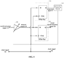
- the metastable state detection device includes: a delay unit 110, a first flip-flop unit 120, a second flip-flop unit 130, and a processing module 140.
- An input terminal of the delay unit 110 is configured to receive a synchronization (SYNC) signal 1A.
- the delay unit 110 receives the synchronization signal 1A, and can delay the synchronization signal 1A.
- the delay unit 110 can perform a corresponding delay on the received synchronization signal 1A.
- the delay unit 110 may include a register or a counter.
- the delay unit 110 may be a register, which is referred to as DSYNC.
- Control bits of the register can be set as ⁇ M-1:0>, wherein M represents the number of the control bits of the register, ⁇ M-1:0> represents that there are M control bits and 2 ⁇ M register values in total.
- the delay value used by the delay unit 110 to perform a delay processing on the synchronization signal 1A is Td ⁇ 1>; when the control value is 1, the delay value used by the delay unit 110 to perform a delay processing on the synchronization signal 1A is Td ⁇ 2>, and so on.
- the delay value used by the delay unit 110 to perform a delay processing on the synchronization signal 1A is Td ⁇ M>.
- each delay value used by the delay unit 110 to perform a delay processing on the synchronization signal 1A is set according to a preset step.
- the delay value Td ⁇ 1> is less than the delay value Td ⁇ 2>
- the delay value Td ⁇ 2> is less than the delay value Td ⁇ 3>.
- the difference between any two adjacent delay value may not the same. In the present invention, the difference between two adjacent delay values is not further limited.
- the first flip-flop unit 120 includes a first clock input terminal, a first data input terminal, and a first data output terminal.
- the second flip-flop unit 130 includes a second clock input terminal, a second data input terminal, and a second data output terminal.
- the first clock input terminal of the first flip-flop unit 120 and the second data input terminal of the second flip-flop unit 130 are connected with each other, both of which are configured to receive a clock signal 1B.
- the first data input terminal of the first flip-flop unit 120 and the second clock input terminal of the second flip-flop unit 130 are both connected to the delay unit 110, both of which are configured to receive a synchronization signal 1A that has been delay processed by the delay unit 110.
- the first flip-flop unit 120 can synchronize the delay processed synchronization signal 1A with the clock signal 1B such that the first data output terminal outputs a target synchronization signal 1D that is synchronized with the clock signal 1B.
- the synchronization signal 1A can be used as a sampling clock
- the clock signal 1B can be used as a data signal. That is, the high frequency clock signal 1B can be sampled with the low frequency synchronization signal 1A, such that the second data output terminal of the second flip-flop unit 130 can output a target clock signal 1C that is synchronized with the delayed synchronization signal 1A to recover the clock signal 1B. That is, the second data output terminal of the second flip-flop unit 130 can be used as a metastable state detection terminal.
- the processing module 140 is connected to the second data output terminal, and is configured to receive the target clock signal 1C, and detect a metastable state of the first flip-flop unit 120 according to the target clock signal 1C.
- the metastable state means that a flip-flop cannot reach a confirmable state within a prescribed period of time.
- the setup time and hold time of the flip-flop define a time window around a clock rising edge. If a data signal at a data input terminal of the flip-flop is changed (or the data is updated) within the time window, a timing violation will be generated, and thus a metastable state will occur.
- the processing module 140 may obtain a level signal of a corresponding target clock signal 1B output from the second data output terminal of the second flip-flop unit 130 (which can be corresponding to a recorded delay value such as Td ⁇ 1>, Td ⁇ 2>,..., ⁇ Td ⁇ 14> as shown in FIG. 2 ) and a level signal of a corresponding target clock signal 1C output from the second data output terminal of the second flip-flop unit 130 (P401, P402, P403,..., P414, and etc. as shown in FIG. 2 ) for each delay value.
- a correspondence relationship between the target clock signal 1C and the delay value can be obtained.
- the point where the first flip-flop unit 120 presents a metastable state can be detected according to the correspondence relationship.
- P407 and P414 are the points where the metastable state is most likely to occur. That is, the first flip-flop unit 120 is most likely to present a metastable state when the delay value is Td ⁇ 7> or Td ⁇ 14>.
- the second data output terminal of the second flip-flop unit 130 can be used as a metastable state detection terminal of the first flip-flop unit 120 to detect a metastable state of the first flip-flop unit 120, which has a simple structure and high detection accuracy.
- the first flip-flop unit 120 and the second flip-flop unit 130 are both D flip-flops.
- the D flip-flop includes 3 data ports, namely D, Q and CLK, wherein D is a data input terminal, Q is a data output terminal, and CLK is a clock input terminal.
- the data input terminal D of the D flip-flop can be used as the first data input terminal of the first flip-flop unit 120 and the second data input terminal of the second flip-flop unit 130;
- the data output terminal Q of the D flip-flop can be used as the first data output terminal of the first flip-flop unit 120 and the second data output terminal of the second flip-flop unit 130;
- the clock input terminal CLK of the D flip-flop can be used as the first clock input terminal of the first flip-flop unit 120 and the second clock input terminal of the second flip-flop unit 130.
- the first flip-flop unit 120 includes a first inverter 121 and a first JK flip-flop 122.
- the J terminal of the first JK flip-flop 122 is connected to the K terminal of the first JK flip-flop 122 via the first inverter 121.
- the clock terminal of the first JK flip-flop 122 is used as the first clock input terminal of the first flip-flop unit 120, and a common connection terminal of the J terminal of the first JK flip-flop 122 and the first inverter 121 is used as the first data input terminal of the first flip-flop unit 120.
- the second flip-flop unit 130 includes a second inverter 131 and a second JK flip-flop 132.
- the J terminal of the second JK flip-flop 132 is connected to the K terminal of the second JK flip-flop 132 via the second inverter 131.
- the clock terminal of the second JK flip-flop 132 is used as the second clock input terminal of the second flip-flop unit 130, and a common connection terminal of the J terminal of the second JK flip-flop unit 132 and the second inverter 131 is used as the second data input terminal of the second flip-flop unit 130. That is, the data output terminal Q of the second JK flip-flop 132 can be used as the metastable state detection terminal of the first JK flip-flop 122 to detect the metastable state of the first JK flip-flop 122.
- a D flip-flop can be composed of a JK flip-flop and an inverter to realize a metastable state detection function.
- the specific implementation of this embodiment is identical to that of the foregoing embodiment, and will not be repeated here.
- first flip-flop unit 120 have a same structural formation as the second flip-flop unit 130, so as to ensure that the output signal of the first flip-flop unit 120 has a same state as that of the second flip-flop unit 130.
- the processing module 140 includes a reading unit and a controller.
- the reading unit is connected to the second data output terminal of the second flip-flop unit 130, and is configured to read the target clock signal 1C output from the second flip-flop unit 130.
- the reading unit may be a SPI reading module, which can read the target clock signal 1C output from the second flip-flop unit 130 to the controller for processing.
- the controller is respectively connected to the reading unit and the delay unit 110, and is configured to detect a metastable state of the first flip-flop unit 120.
- the controller may be a processor of an external device that is capable of processing the target clock signal 1C, such as a CPU, a MCU, or an FPGA.
- the controller can also obtain a calibration delay value for calibrating the metastable state according to the target clock signal 1C, and is also configured to control the delay unit 110 to delay the synchronization signal 1A by the calibration delay value.
- P407 P4114 is a metastable point of the first flip-flop unit 120. A farthest point from the two metastable state points P407 and P414 is the midpoint P410 between them. Further, P403 is also a point farthest from the metastable state P407. Accordingly, P410 and P407 can also be understood as points with a largest margin. The point P403 or P410 with a largest margin can be used as the calibration delay value.
- the controller can take the delay value corresponding to a position (P403 or P410) where logic "1" is changed to logical “0” to be a calibration delay value according to the level signal (P401, P402, P403,..., P414 and etc. as shown in FIG. 2 ) of the target clock signal 1C output from the second data output terminal.
- the controller may set the control bits ⁇ M-1:0> of the delay unit 110 to be a fixed calibration delay value, such that the delay unit 110 can delay the synchronization signal 1A with the calibration delay value.
- the metastable state detection device can also obtain a corresponding correction delay value, and calibrate the metastable state of the first flip-flop unit 120 according to the calibration delay value, so as to remove the metastable state of the first flip-flop unit 120 and thus improve the performance of the first flip-flop unit 120.
- the metastable state detection device in the above embodiment can implement the detection of a metastable state that occurs when a plurality of clock modules is synchronized. By adjusting the delay and detecting the target clock signal 1C that is output after the delay is performed, the calibration of the data synchronization is achieved.
- the metastable state detection device can be arranged outside an ADC, or integrated into an ADC to form an ADC with a metastable detection function.
- the metastable state detection device can be arranged within a Field Programmable Gate Array (FPGA). Both the clock signal 1B and the synchronization signal 1A of the metastable state detection device can be generated by the FPGA.
- the first data output terminal of the first flip-flop unit 120 can be connected to a module A within the FPGA that need to use the clock signal 1B.
- the first data output terminal of the first flip-flop unit 120 can be connected to a reset RST signal of the module A. That is, a low frequency synchronization signal 1A can be used to sample a high frequency clock signal 1B, and the clock signal 1B can be finally recovered.
- the metastable state detection device When the metastable state detection device is built in the FPGA, the detection of a metastable state that occurs when a plurality of clock modules is synchronized can be implemented. By adjusting the delay and detecting the target clock signal 1C that is output after the delay is performed, the calibration of the data synchronization can be achieved.
- the metastable state detection device is also applicable to other electronic devices that need to synchronize a plurality of clock modules.
- an ADC circuit is also provided in the embodiments of the present application.
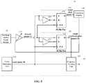
- the ADC circuit includes a clock module 20, a synchronization signal module 30, and a metastable state detection device 10 in any of the above embodiments.
- the clock module 20 is configured to output a clock signal 1B.
- the clock module 20 includes a clock generating unit 210 and a frequency dividing unit 220.
- the clock generating unit 210 is respectively connected to the first clock input terminal and the second data input terminal, and is configured to provide a generated clock signal 1B to the first flip-flop unit 120 and the second flip-flop unit 130;
- the frequency dividing unit 220 is respectively connected to the clock generating unit 210 and the first data output terminal, and is configured to perform a frequency dividing processing on a target synchronization signal 1D output from the first flip-flop unit 120.
- the clock generating unit 210 may be a clock distributor with a phase-locked loop, and may output a plurality of channels of clock signals 1B.
- the frequency dividing unit 220 may be a frequency divider, and may perform a 4 or 8 frequency dividing processing on the target synchronization signal 1D output from the first flip-flop unit 120.
- the synchronization signal module 30 is configured to output a synchronization signal 1A.
- the metastable state detection device 10 includes a delay unit 110, a first flip-flop unit 120, a second flip-flop unit 130 and a processing module 140.
- An input terminal of the delay unit 110 is connected to the synchronization signal module 30, and an output terminal of the delay unit 110 is respectively connected to the first data input terminal and the second clock input terminal.
- the first clock input terminal, the second data input terminal, and the first data output terminal are respectively connected to the clock module 20.
- the metastable state detection device 10 is arranged in the ADC circuit, wherein the second data input terminal of the second flip-flop unit 130 is connected to the first clock input terminal of the first flip-flop unit 120 in the metastable state detection device 10.
- the second data output terminal of the second flip-flop unit 130 can be used as the metastable state detection terminal of the first flip-flop unit 120 to detect the metastable state of the first flip-flop unit 120.
- the ADC circuit has a metastable detection function, and has a simple structure and high detection accuracy.
- the embodiment of the application also provides a metastable state detection method.
- the metastable state detection method is applicable to a metastable state detection device.
- the metastable state detection device includes a delay unit 110, a first flip-flop unit 120, and a second flip-flop unit 130.
- the clock input terminal of the first flip-flop unit is connected to the data input terminal of the second flip-flop unit, both of which are configured to receive a clock signal 1B.
- the data input terminal of the first flip-flop unit and the clock input terminal of the second flip-flop unit are respectively connected to the delay unit, both of which are configured to receive a delay processed synchronization signal 1A.
- the metastable state detection method includes step 602-step 606, in which:
- Step 602 the delay unit is controlled to delay the received synchronization signal based on preset delay values
- the delay unit may include a register, which is referred to as DSYNC.
- Control bits of the register can be set as ⁇ M-1:0>, wherein M represents the number of the control bits of the register, ⁇ M-1:0> represents that there are M control bits and 2 ⁇ M register values in total.
- M represents the number of the control bits of the register
- ⁇ M-1:0> represents that there are M control bits and 2 ⁇ M register values in total.
- the delay value used by the delay unit 110 to perform a delay processing on the synchronization signal 1A is Td ⁇ M>.
- each delay value used by the delay unit 110 to perform a delay processing on the synchronization signal 1A is set according to a preset step.
- the delay value Td ⁇ 1> is less than the delay value Td ⁇ 2>
- the delay value Td ⁇ 2> is less than the delay value Td ⁇ 3>.
- the difference between any two adjacent delay values may not be the same. In the present invention, the difference between two adjacent delay values is not further limited.
- Step 604 target clock signals from the second flip-flop unit is recorded in correspondence with each of the delay values.
- the delay values (Td ⁇ 1>, Td ⁇ 2>,..., ⁇ Td ⁇ 14> in FIG. 2 ) can be recorded in correspondence with the level signals (P401, P402, P403,..., P414, and etc. in FIG. 2 ) of the target clock signal 1B output from the second data output terminal can be recorded.
- Step 606 a metastable state of the first flip-flop unit is detected according to the recorded correspondence relationships between the delay values and the target clock signals.
- a metastable state of the first flip-flop unit is detected according to the recorded correspondence relationships between the delay values and the target clock signals includes:
- a delay value within a setup/hold time window (a window where the metastable state is most likely to occur) is used as the detected metastable state according to the relationships between the delay values and the clock phase outputs.
- the correspondence relationships between the target clock signals 1C and the delay values can be obtained, and points where the first flip-flop unit presents a metastable state can be detected according to the correspondence relationships.
- P407 and P414 are the points where a metastable state is most likely to occur. That is, the first flip-flop unit is most likely to present a metastable state when the delay value is Td ⁇ 7> or Td ⁇ 14>.
- the metastable state detection method further includes a step of calibrating the metastable state of the first flip-flop unit.
- calibrating the metastable state of the first flip-flop unit includes:
- Step 702 a delay value within a window where logic "1" previous to a transition is transitioned to logic "0" next to the transition is obtained according to a recorded clock signal.
- Step 704 the delay value corresponding to the transition from logic "1" previous to the transition to logic "0" next to the transition is taken to be a calibration value.
- P407 (P414) is the metastable state point of the first flip-flop unit.
- a farthest point from the two metastable state points P407 and P414 is the midpoint P410 between them.
- P403 is also a farthest point from the metastable state point P407.
- P410 and P407 can be understood as points with a largest margin, and the point P403 or P410 with a largest margin can be used as the calibration delay value.
- the controller can take the delay value that is corresponding to a position (P403 or P410) where logic "1" previous to a transition is transitioned to logic "0" next to the transition to be a calibration delay value according to the level signal (P401, P402, P403,..., P414 and etc. in FIG. 2 ) of the target clock signal 1C output from the second data output terminal.
- Step 706 the delay unit is controlled to delay the synchronization signal 1A with the calibration value.
- the control bits ⁇ M-1:0> of the delay unit are set to be a fixed calibration delay value, such that the delay unit delays the synchronization signal 1A with the calibration delay value.
- a calibration value of the minimum value is selected to be the target calibration value.
- the control bits ⁇ M-1:0> of the delay unit is set to be the fixed target calibration value, such that the delay unit delays the synchronization signal 1A for the target calibration value. As a result, the metastable state of the first flip-flop unit is eliminated.
- a corresponding calibration delay value can further be obtained, and the metastable state of the first flip-flop unit can be calibrated based on the calibration delay value, such that the metastable state of the first flip-flop unit is eliminated and thus the performance of the first flip-flop unit is improved.
- the metastable state detection method further includes: detecting if a clock mode of the clock signal 1B has been changed; and when the clock mode has been changed, recalibrating the metastable state of the first flip-flop unit.
- the clock mode can include single-channel mode, dual-channel mode, four-channel mode, and other modes.
- the phase of its clock signal 1B will also be changed.
- the metastable state of the first flip-flop unit is required to be recalibrated.
- steps of the recalibration reference can be made to the above-mentioned steps 702 to 706, which will not be repeated herein.
- the metastable state of the first flip-flop unit may be recalibrated to improve the performance of the first flip-flop unit.
Landscapes
- Engineering & Computer Science (AREA)
- Theoretical Computer Science (AREA)
- Synchronisation In Digital Transmission Systems (AREA)
- Pulse Circuits (AREA)
- Manipulation Of Pulses (AREA)
Applications Claiming Priority (2)
| Application Number | Priority Date | Filing Date | Title |
|---|---|---|---|
| CN201911366573.5A CN111262583B (zh) | 2019-12-26 | 2019-12-26 | 亚稳态检测装置和方法、adc电路 |
| PCT/CN2020/089478 WO2021128701A1 (fr) | 2019-12-26 | 2020-05-09 | Dispositif et procédé de détection d'état métastable et circuit can |
Publications (2)
| Publication Number | Publication Date |
|---|---|
| EP3872995A1 true EP3872995A1 (fr) | 2021-09-01 |
| EP3872995A4 EP3872995A4 (fr) | 2022-08-31 |
Family
ID=70948521
Family Applications (1)
| Application Number | Title | Priority Date | Filing Date |
|---|---|---|---|
| EP20859675.9A Pending EP3872995A4 (fr) | 2019-12-26 | 2020-05-09 | Dispositif et procédé de détection d'état métastable et circuit can |
Country Status (5)
| Country | Link |
|---|---|
| US (1) | US11451236B2 (fr) |
| EP (1) | EP3872995A4 (fr) |
| JP (1) | JP7214855B2 (fr) |
| CN (1) | CN111262583B (fr) |
| WO (1) | WO2021128701A1 (fr) |
Cited By (1)
| Publication number | Priority date | Publication date | Assignee | Title |
|---|---|---|---|---|
| CN119603107A (zh) * | 2025-01-24 | 2025-03-11 | 四川天邑康和通信股份有限公司 | 低压差分信号的降采样方法和装置、电子设备及存储介质 |
Families Citing this family (3)
| Publication number | Priority date | Publication date | Assignee | Title |
|---|---|---|---|---|
| CN112332834B (zh) * | 2021-01-04 | 2021-04-13 | 南京芯视界微电子科技有限公司 | 激光雷达的时间数字转换器避免亚稳态的矫正方法及装置 |
| CN121091960A (zh) * | 2024-06-06 | 2025-12-09 | 普源精电科技股份有限公司 | 一种时钟同步系统 |
| CN118590067B (zh) * | 2024-08-08 | 2024-11-08 | 合肥健天电子有限公司 | 一种模数接口采样电路及采样方法 |
Family Cites Families (38)
| Publication number | Priority date | Publication date | Assignee | Title |
|---|---|---|---|---|
| US5122694A (en) * | 1990-12-26 | 1992-06-16 | Tektronix, Inc. | Method and electrical circuit for eliminating time jitter caused by metastable conditions in asynchronous logic circuits |
| US6265904B1 (en) * | 1998-10-02 | 2001-07-24 | Vlsi Technology Inc. | Digital phase shift amplification and detection system and method |
| JP2002107381A (ja) * | 2000-10-02 | 2002-04-10 | Teratekku:Kk | コヒーレント・サンプリング方法と装置 |
| US7430141B2 (en) * | 2004-11-16 | 2008-09-30 | Texas Instruments Incorporated | Method and apparatus for memory data deskewing |
| KR100886354B1 (ko) * | 2007-05-17 | 2009-03-03 | 삼성전자주식회사 | 다중 위상 클럭신호를 사용하는 통신 시스템 및 통신 방법 |
| US8471754B2 (en) * | 2008-08-01 | 2013-06-25 | Advantest Corporation | Time measurement circuit |
| CN101860353B (zh) * | 2010-06-17 | 2012-02-29 | 广州市广晟微电子有限公司 | 数模混合芯片中的时钟电路控制装置及方法 |
| JP2012244521A (ja) * | 2011-05-23 | 2012-12-10 | Keio Gijuku | 比較器及びad変換器 |
| ITTO20110485A1 (it) * | 2011-06-03 | 2012-12-04 | Torino Politecnico | Method and circuit for solving metastability conditions and recovering signal errors in digitalintegrated circuits |
| CN103095289B (zh) * | 2011-11-08 | 2015-03-04 | 澜起科技(上海)有限公司 | 一种信号延迟控制电路 |
| TWI448081B (zh) * | 2012-01-20 | 2014-08-01 | Nat Univ Chung Cheng | All-digital clock correction circuit and method thereof |
| US9020084B2 (en) * | 2013-01-31 | 2015-04-28 | Qualcomm Incorporated | High frequency synchronizer |
| US8872691B1 (en) * | 2013-05-03 | 2014-10-28 | Keysight Technologies, Inc. | Metastability detection and correction in analog to digital converter |
| US8957802B1 (en) * | 2013-09-13 | 2015-02-17 | Cadence Design Systems, Inc. | Metastability error detection and correction system and method for successive approximation analog-to-digital converters |
| CN103746698B (zh) * | 2014-01-28 | 2017-02-01 | 华为技术有限公司 | 模数转换器 |
| PL223881B1 (pl) * | 2014-02-07 | 2016-11-30 | Politechnika Warszawska | Układ fizycznie nieklonowalnej funkcji |
| CN104320138A (zh) * | 2014-08-29 | 2015-01-28 | 成都锐成芯微科技有限责任公司 | 全异步sar adc亚稳态消除电路与方法 |
| KR20170005330A (ko) * | 2015-07-03 | 2017-01-12 | 에스케이하이닉스 주식회사 | 클럭 생성 회로 및 방법, 이를 이용한 반도체 장치 및 전자 시스템 |
| CN105159374B (zh) * | 2015-08-31 | 2016-09-21 | 东南大学 | 面向超宽电压的在线监测单元及监测窗口自适应调节系统 |
| CN105187053B (zh) * | 2015-09-07 | 2017-12-22 | 电子科技大学 | 一种用于tdc的亚稳态消除电路 |
| US10038450B1 (en) * | 2015-12-10 | 2018-07-31 | Xilinx, Inc. | Circuits for and methods of transmitting data in an integrated circuit |
| CN106537786B (zh) * | 2016-05-05 | 2019-03-19 | 香港应用科技研究院有限公司 | 同步系统里的异步逐次逼近寄存器模数转换器(sar adc) |
| US9899992B1 (en) * | 2016-08-17 | 2018-02-20 | Advanced Micro Devices, Inc. | Low power adaptive synchronizer |
| US9634680B1 (en) * | 2016-10-24 | 2017-04-25 | Keysight Technologies, Inc. | Large-error detection and correction of digital sample sequence from analog-to-digital converter |
| US10175655B2 (en) * | 2017-03-17 | 2019-01-08 | Intel Corporation | Time-to-digital converter |
| WO2019117803A1 (fr) * | 2017-12-14 | 2019-06-20 | Huawei International Pte. Ltd. | Convertisseur temps-numérique |
| CN110311659B (zh) * | 2018-03-27 | 2021-02-12 | 华为技术有限公司 | 一种触发器及集成电路 |
| CN110504968B (zh) * | 2018-05-17 | 2023-03-24 | 四川锦江电子医疗器械科技股份有限公司 | 一种双异步信号采样计数装置与方法 |
| CN109032498B (zh) * | 2018-07-25 | 2021-03-30 | 电子科技大学 | 一种多fpga的多通道采集系统的波形量化同步方法 |
| CN109150182B (zh) * | 2018-08-28 | 2021-10-26 | 电子科技大学 | 一种适用于比较器的亚稳态检测电路 |
| CN110912539B (zh) * | 2018-09-14 | 2025-02-21 | 恩智浦美国有限公司 | 时钟发生器和产生时钟信号的方法 |
| US10928447B2 (en) * | 2018-10-31 | 2021-02-23 | Taiwan Semiconductor Manufacturing Co., Ltd. | Built-in self test circuit for measuring phase noise of a phase locked loop |
| CN109995359B (zh) * | 2019-04-10 | 2023-03-28 | 侯凤妹 | 边沿触发器亚稳态观测系统及其观测方法 |
| CN110401443B (zh) * | 2019-06-25 | 2023-03-31 | 中国科学院上海微系统与信息技术研究所 | 同步时钟adc电路的亚稳态的检测消除电路 |
| CN110401444B (zh) * | 2019-06-25 | 2023-04-07 | 中国科学院上海微系统与信息技术研究所 | 异步时钟adc电路的亚稳态的检测消除电路 |
| TWI716975B (zh) * | 2019-08-21 | 2021-01-21 | 智原科技股份有限公司 | 時間偵測電路及時間偵測方法 |
| US10999050B1 (en) * | 2020-05-04 | 2021-05-04 | Stmicroelectronics International N.V. | Methods and apparatus for data synchronization in systems having multiple clock and reset domains |
| US10848140B1 (en) * | 2020-07-20 | 2020-11-24 | Nxp Usa, Inc. | Method and system for detecting clock failure |
-
2019
- 2019-12-26 CN CN201911366573.5A patent/CN111262583B/zh active Active
-
2020
- 2020-05-09 JP JP2021518702A patent/JP7214855B2/ja active Active
- 2020-05-09 EP EP20859675.9A patent/EP3872995A4/fr active Pending
- 2020-05-09 US US17/276,027 patent/US11451236B2/en active Active
- 2020-05-09 WO PCT/CN2020/089478 patent/WO2021128701A1/fr not_active Ceased
Cited By (1)
| Publication number | Priority date | Publication date | Assignee | Title |
|---|---|---|---|---|
| CN119603107A (zh) * | 2025-01-24 | 2025-03-11 | 四川天邑康和通信股份有限公司 | 低压差分信号的降采样方法和装置、电子设备及存储介质 |
Also Published As
| Publication number | Publication date |
|---|---|
| JP2022517895A (ja) | 2022-03-11 |
| CN111262583B (zh) | 2021-01-29 |
| CN111262583A (zh) | 2020-06-09 |
| EP3872995A4 (fr) | 2022-08-31 |
| JP7214855B2 (ja) | 2023-01-30 |
| US11451236B2 (en) | 2022-09-20 |
| WO2021128701A1 (fr) | 2021-07-01 |
| US20220109450A1 (en) | 2022-04-07 |
Similar Documents
| Publication | Publication Date | Title |
|---|---|---|
| EP3872995A1 (fr) | Dispositif et procédé de détection d'état métastable et circuit can | |
| US8824224B2 (en) | Frequency-agile strobe window generation | |
| US9628258B2 (en) | Clock generation circuit and method and semiconductor apparatus and electronic system using the same | |
| CN109254941B (zh) | 基于fpga的串行信号时钟同步方法、串转并方法及装置 | |
| US8594264B1 (en) | Phase detection and aligned signal selection with multiple phases of clocks | |
| US20010018751A1 (en) | Integrated data clock extractor | |
| KR101076109B1 (ko) | 패턴 삽입을 이용한 수신 데이터의 스큐 보정 방법 및 그 장치 | |
| US8504865B2 (en) | Dynamic phase alignment | |
| CN212622809U (zh) | 检测电路 | |
| US8711996B2 (en) | Methods and apparatus for determining a phase error in signals | |
| US7430141B2 (en) | Method and apparatus for memory data deskewing | |
| US20240313748A1 (en) | Sampling signals | |
| US6937953B2 (en) | Circuit configuration for receiving at least two digital signals | |
| US20050146365A1 (en) | Apparatus for generating internal clock signal | |
| CN114076849B (zh) | 检测电路和检测方法 | |
| US20130294555A1 (en) | Method and apparatus for deskewing data transmissions | |
| JP2008047118A (ja) | 受信ウィンドウの位置確認方法および受信ウィンドウの位置確認装置 | |
| CN116192355B (zh) | Mipi发送器及其时钟校准方法 | |
| US20040128603A1 (en) | Device for testing the conformity of an electronic connection | |
| EP4012423B1 (fr) | Circuit de détection et procédé de détection | |
| US11804825B1 (en) | System and method of compensating for voltage and temperature variations in communication link | |
| US10225115B1 (en) | Low-frequency periodic signal detector | |
| RU2806240C1 (ru) | Схема обнаружения и способ обнаружения | |
| US20230307021A1 (en) | Data reading/writing circuit, method, and device | |
| US7091764B2 (en) | Duty distortion detector |
Legal Events
| Date | Code | Title | Description |
|---|---|---|---|
| STAA | Information on the status of an ep patent application or granted ep patent |
Free format text: STATUS: UNKNOWN |
|
| STAA | Information on the status of an ep patent application or granted ep patent |
Free format text: STATUS: THE INTERNATIONAL PUBLICATION HAS BEEN MADE |
|
| PUAI | Public reference made under article 153(3) epc to a published international application that has entered the european phase |
Free format text: ORIGINAL CODE: 0009012 |
|
| STAA | Information on the status of an ep patent application or granted ep patent |
Free format text: STATUS: REQUEST FOR EXAMINATION WAS MADE |
|
| 17P | Request for examination filed |
Effective date: 20210312 |
|
| AK | Designated contracting states |
Kind code of ref document: A1 Designated state(s): AL AT BE BG CH CY CZ DE DK EE ES FI FR GB GR HR HU IE IS IT LI LT LU LV MC MK MT NL NO PL PT RO RS SE SI SK SM TR |
|
| REG | Reference to a national code |
Ref country code: DE Ref legal event code: R079 Free format text: PREVIOUS MAIN CLASS: H03M0001100000 Ipc: H03M0001080000 |
|
| A4 | Supplementary search report drawn up and despatched |
Effective date: 20220803 |
|
| RIC1 | Information provided on ipc code assigned before grant |
Ipc: H03M 1/12 20060101ALI20220728BHEP Ipc: H03M 1/08 20060101AFI20220728BHEP |
|
| DAV | Request for validation of the european patent (deleted) | ||
| DAX | Request for extension of the european patent (deleted) | ||
| P01 | Opt-out of the competence of the unified patent court (upc) registered |
Effective date: 20230530 |
|
| STAA | Information on the status of an ep patent application or granted ep patent |
Free format text: STATUS: EXAMINATION IS IN PROGRESS |
|
| 17Q | First examination report despatched |
Effective date: 20240527 |
|
| GRAP | Despatch of communication of intention to grant a patent |
Free format text: ORIGINAL CODE: EPIDOSNIGR1 |
|
| STAA | Information on the status of an ep patent application or granted ep patent |
Free format text: STATUS: GRANT OF PATENT IS INTENDED |
|
| INTG | Intention to grant announced |
Effective date: 20260130 |