EP3876154B1 - Procédé d'identification de carte mémoire et dispositif mobile - Google Patents
Procédé d'identification de carte mémoire et dispositif mobile Download PDFInfo
- Publication number
- EP3876154B1 EP3876154B1 EP19903739.1A EP19903739A EP3876154B1 EP 3876154 B1 EP3876154 B1 EP 3876154B1 EP 19903739 A EP19903739 A EP 19903739A EP 3876154 B1 EP3876154 B1 EP 3876154B1
- Authority
- EP
- European Patent Office
- Prior art keywords
- memory card
- card
- command
- type memory
- identified
- Prior art date
- Legal status (The legal status is an assumption and is not a legal conclusion. Google has not performed a legal analysis and makes no representation as to the accuracy of the status listed.)
- Active
Links
Images


Classifications
-
- G—PHYSICS
- G06—COMPUTING OR CALCULATING; COUNTING
- G06F—ELECTRIC DIGITAL DATA PROCESSING
- G06F13/00—Interconnection of, or transfer of information or other signals between, memories, input/output devices or central processing units
- G06F13/38—Information transfer, e.g. on bus
- G06F13/382—Information transfer, e.g. on bus using universal interface adapter
- G06F13/385—Information transfer, e.g. on bus using universal interface adapter for adaptation of a particular data processing system to different peripheral devices
-
- G—PHYSICS
- G06—COMPUTING OR CALCULATING; COUNTING
- G06K—GRAPHICAL DATA READING; PRESENTATION OF DATA; RECORD CARRIERS; HANDLING RECORD CARRIERS
- G06K19/00—Record carriers for use with machines and with at least a part designed to carry digital markings
- G06K19/06—Record carriers for use with machines and with at least a part designed to carry digital markings characterised by the kind of the digital marking, e.g. shape, nature, code
- G06K19/067—Record carriers with conductive marks, printed circuits or semiconductor circuit elements, e.g. credit or identity cards also with resonating or responding marks without active components
- G06K19/07—Record carriers with conductive marks, printed circuits or semiconductor circuit elements, e.g. credit or identity cards also with resonating or responding marks without active components with integrated circuit chips
- G06K19/0722—Record carriers with conductive marks, printed circuits or semiconductor circuit elements, e.g. credit or identity cards also with resonating or responding marks without active components with integrated circuit chips comprising an arrangement for testing the record carrier
-
- G—PHYSICS
- G06—COMPUTING OR CALCULATING; COUNTING
- G06F—ELECTRIC DIGITAL DATA PROCESSING
- G06F13/00—Interconnection of, or transfer of information or other signals between, memories, input/output devices or central processing units
- G06F13/10—Program control for peripheral devices
- G06F13/102—Program control for peripheral devices where the program performs an interfacing function, e.g. device driver
-
- G—PHYSICS
- G06—COMPUTING OR CALCULATING; COUNTING
- G06K—GRAPHICAL DATA READING; PRESENTATION OF DATA; RECORD CARRIERS; HANDLING RECORD CARRIERS
- G06K19/00—Record carriers for use with machines and with at least a part designed to carry digital markings
- G06K19/06—Record carriers for use with machines and with at least a part designed to carry digital markings characterised by the kind of the digital marking, e.g. shape, nature, code
- G06K19/067—Record carriers with conductive marks, printed circuits or semiconductor circuit elements, e.g. credit or identity cards also with resonating or responding marks without active components
- G06K19/07—Record carriers with conductive marks, printed circuits or semiconductor circuit elements, e.g. credit or identity cards also with resonating or responding marks without active components with integrated circuit chips
- G06K19/077—Constructional details, e.g. mounting of circuits in the carrier
- G06K19/0772—Physical layout of the record carrier
- G06K19/07732—Physical layout of the record carrier the record carrier having a housing or construction similar to well-known portable memory devices, such as SD cards, USB or memory sticks
-
- G—PHYSICS
- G06—COMPUTING OR CALCULATING; COUNTING
- G06K—GRAPHICAL DATA READING; PRESENTATION OF DATA; RECORD CARRIERS; HANDLING RECORD CARRIERS
- G06K19/00—Record carriers for use with machines and with at least a part designed to carry digital markings
- G06K19/06—Record carriers for use with machines and with at least a part designed to carry digital markings characterised by the kind of the digital marking, e.g. shape, nature, code
- G06K19/067—Record carriers with conductive marks, printed circuits or semiconductor circuit elements, e.g. credit or identity cards also with resonating or responding marks without active components
- G06K19/07—Record carriers with conductive marks, printed circuits or semiconductor circuit elements, e.g. credit or identity cards also with resonating or responding marks without active components with integrated circuit chips
- G06K19/077—Constructional details, e.g. mounting of circuits in the carrier
- G06K19/07743—External electrical contacts
-
- G—PHYSICS
- G06—COMPUTING OR CALCULATING; COUNTING
- G06K—GRAPHICAL DATA READING; PRESENTATION OF DATA; RECORD CARRIERS; HANDLING RECORD CARRIERS
- G06K7/00—Methods or arrangements for sensing record carriers, e.g. for reading patterns
- G06K7/0013—Methods or arrangements for sensing record carriers, e.g. for reading patterns by galvanic contacts, e.g. card connectors for ISO-7816 compliant smart cards or memory cards, e.g. SD card readers
-
- G—PHYSICS
- G06—COMPUTING OR CALCULATING; COUNTING
- G06K—GRAPHICAL DATA READING; PRESENTATION OF DATA; RECORD CARRIERS; HANDLING RECORD CARRIERS
- G06K7/00—Methods or arrangements for sensing record carriers, e.g. for reading patterns
- G06K7/0013—Methods or arrangements for sensing record carriers, e.g. for reading patterns by galvanic contacts, e.g. card connectors for ISO-7816 compliant smart cards or memory cards, e.g. SD card readers
- G06K7/0052—Methods or arrangements for sensing record carriers, e.g. for reading patterns by galvanic contacts, e.g. card connectors for ISO-7816 compliant smart cards or memory cards, e.g. SD card readers connectors capable of contacting cards of different formats, e.g. memory stick and SD card readers sharing at least one connector contact and the associated signal line, e.g. both using the same signal line for input or output of data
Definitions
- This application relates to the field of storage technologies, and in particular, to a memory card identification method and a mobile device.
- memory cards are supported by more and more terminal devices.
- a terminal device loads data to the memory card by using an identification program, to identify the memory card.
- a CMD8 command and an ACMD41 command are usually used to determine whether the SD card responds, so as to identify the SD card. This manner is implemented through two steps, and therefore is relatively slow and has relatively low identification efficiency.
- US 2005 / 251 593 A1 describes a memory card that comprises a multiple interface controller, comprising at least a USB processor, MMC/HS MMC processor and SD processor, and each processor individually connected to a data r/w controller and a shared interface bus, the data r/w controller connected to at least a data-storage medium, and shared interface bus connected to a computer system or IA product.
- a method of controlling a SIM card and SD card that may determine a card having a high priority and that may determine whether to reset a card, when a different plurality of memory cards are inserted, is known from EP 3 197 059 A1 .
- the present invention provides a memory card identification method and a mobile device according to the independent claims. Particular embodiments are specified in the dependent claims.
- This application further provides a memory card identification method and a mobile device, to resolve a prior-art problem that different memory cards are identified at a relatively slow speed.
- a memory card identification method comprising: sending an initialization command of a first-type memory card communications protocol to a to-be-identified memory card; detecting whether there is a response; and identifying the memory card; characterized in that the response is a response on a command pin of the memory card and the memory card is identified as a first-type memory card or a second-type memory card based on a response status of the command pin; wherein the method further comprises before the step of sending an initialization command of a first-type memory card communications protocol to a to-be-identified memory card: powering on a DAT3 pin of the to-be-identified memory card, so that the DAT3 pin is in a non-grounded state.
- the method further includes: sending a reset command shared by the first-type memory card communications protocol and the second-type memory card communications protocol to the command pin of the to-be-identified memory card, so that the to-be-identified memory card enters an idle state.
- the step of identifying the memory card as a first-type memory card or a second-type memory card based on a response status of the command pin includes: identifying the memory card as the first-type memory card if there is a response; or identifying the memory card as the second-type memory card if there is no response.
- the method further includes: initializing the first-type memory card by using the initialization command of the first-type memory card communications protocol.
- the method further includes: initializing the second-type memory card by using an initialization command of a second-type memory card communications protocol.
- a first type memory card is an MMC card
- a second type memory card is an SD card.
- the reset command is a CMD0 command.
- the method further includes: powering on the memory card.
- the initialization command is a CMD1 command.
- a mobile device wherein the mobile device comprises a controller and a card tray that can be embedded into a body of the mobile device, a card slot is disposed on the card tray, the card slot is configured to accommodate a memory card and electrically connect the memory card and the controller, and the controller is configured to identify the memory card by using the foregoing method.
- an MMC protocol type card is identified by using a protocol feature of the MMC card. This implementation can shorten an identification procedure and accelerate an identification speed.
- a memory card is an independent storage medium used in a mobile phone, a digital camera, a portable computer, MP3, and other digital products.
- the memory card is usually in a card form, and therefore is collectively referred to as a "memory card”, also known as a "digital memory card”, a “digital memory card”, a “storage card”, or the like.
- FIG. 1 is a schematic flowchart of a first embodiment of a memory card identification method according to this application. The method includes the following steps.
- Step 11 Send an initialization command of a first-type memory card communications protocol to a to-be-identified memory card.
- Step 12 Detect whether there is a response in a command pin of the memory card.
- this embodiment is mainly used for memory cards that use different communications protocols, and different communications protocols have different initialization manners.
- a communications protocol used by a first-type memory card is the first-type memory card communications protocol, and the initialization command of the first-type memory card communications protocol is a command A; and a communications protocol used by a second-type memory card is a second-type memory card communications protocol, and an initialization command of the second-type memory card communications protocol is a command B.
- the command A is sent to the to-be-identified memory card, only the first-type memory card responds, and the second-type memory card does not respond.
- the command B is sent to the to-be-identified memory card, only the second-type memory card responds, and the first-type memory card does not respond.
- Step 13 Identify the memory card as a first-type memory card or a second-type memory card based on a response status of the command pin.
- the memory card identification method includes: sending the initialization command of the first-type memory card communications protocol to the to-be-identified memory card; detecting whether there is a response in the command pin of the memory card; and identifying the memory card as the first-type memory card or the second-type memory card based on the response status of the command pin.
- a first type memory card is an MMC card and a second type memory card is an SD card.
- the SD card (Secure Digital Memory Card) is a new-generation memory device based on a semiconductor flash memory, and is characterized with a high memory capacity, a fast data transmission rate, great mobility, and high security.
- the SD card usually includes a standard SD card and a micro SD card.
- the MMC is an abbreviation of MultiMediaCard, namely, a multimedia card.
- the MMC is a non-volatile storage device, is characterized with a small size, a large capacity, low power consumption, and a fast transmission speed, and is widely applied to consumer electronics.
- the MMC is an interface agreement (a card type), and a memory that conforms to this interface can be referred to as an mmc memory (mmc card).
- the following describes an identification method of the MMC card and the SD card.
- the MMC card has a total of seven pins, and the seven pins are classified into two operation modes: an MMC mode (also referred to as an MMC identification mode) and an SPI mode.
- MMC mode also referred to as an MMC identification mode
- SPI mode an SPI mode
- the MMC mode mainly includes the following three states:
- the pins of the MMC card are shown in the following table: Pin number Name Function (MMC mode) Function (SPI mode) 1 RES/CS Reset Chip select 2 CMD/DI Command Master-Out-Slave-In 3 VSS1 GND GND 4 VDD Power supply Power supply 5 CLK Clock Clock 6 VSS2 GND GND 7 DAT/DO Data Master-In-Slave-Out
- the SD card has nine pins, and the nine pins are classified into two operation modes: an SD mode and an SPI mode.
- the SD card is mainly run in the SD mode. Therefore, a DAT3 pin of the SD card cannot be grounded, so that the SD card can be prevented from being switched to the SPI mode.
- a DAT3 pin of the to-be-identified memory card is powered on, so that the DAT3 pin is in a non-grounded state.
- the pins of the SD card are shown in the following table: Pin number Name Function (SD mode) Function (SPI mode) 1 DAT3/CS Data 3 Chip select 2 CMD/DI Command Master-Out-Slave-In 3 VSS1 GND GND 4 VDD Power supply Power supply 5 CLK Clock Clock 6 VSS2 GND GND 7 DAT0/DO Data 0 Master-In-Slave-Out 8 DAT1/IRQ Data 1 Reserved 9 DAT2/NC Data 2 Reserved
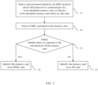
- FIG. 2 is a schematic flowchart of a second embodiment of a memory card identification method according to this application. The method includes the following steps.
- Step 21 Send an initialization command of an MMC protocol to a to-be-identified memory card.
- Commands in an SPI mode are a subset of commands in an MMC mode, but there are fewer commands in the SPI mode than in the MMC mode.
- a host distinguishes the MMC card and the SD card by sending a CMD1 command and a CMD41 command.
- the CMD1 command is sent, and if success information is returned, it indicates that the to-be-identified memory card is the MMC card. Otherwise, the CMD41 command is sent, and if success information is returned, it indicates that the to-be-identified memory card is the SD card.
- Step 22 Detect whether there is a response in a command pin of the memory card.
- step 23 is performed. If there is no response, step 24 is performed.
- Step 23 Identify the memory card as an MMC card.
- Step 24 Identify the memory card as an SD card.
- whether there is a response in a CMD pin of the to-be-detected memory card is detected by sending a CMD1 command.
- the memory card is identified as the MMC card if there is a response.
- the memory card is identified as the SD card if there is no response.
- the detection manner in this embodiment is mainly to determine whether the to-be-identified memory card is the MMC card, and the foregoing command is responded to through the CMD pin. Therefore, only the seventh pin needs to be detected, and the to-be-identified memory card may be determined as the SD card if there is no response.
- a corresponding initialization procedure may be further performed on the memory card. Specifically, after the memory card is identified as the MMC card, the MMC card is initialized by using the initialization command of the MMC protocol. After the memory card is identified as the SD card, the SD card is initialized by using an initialization command of an SD protocol.
- the memory card identification method provided in this embodiment includes: sending the initialization command of the MMC protocol to the to-be-identified memory card; detecting whether there is a response in the command pin of the memory card; and identifying the memory card as the MMC card or the SD card based on a response status of the command pin.
- an MMC protocol type card is identified by using a protocol feature of the MMC card. This implementation can shorten an identification procedure and accelerate an identification speed.
- FIG. 3 is a schematic flowchart of a third embodiment of a memory card identification method according to this application. The method includes the following steps.
- Step 31 Send a reset command shared by an MMC protocol and an SD protocol to a command pin of a to-be-identified memory card, so that the to-be-identified memory card enters an idle state.
- the reset command is a CMD0.
- Step 32 Send a CMD1 command to the memory card.
- Step 33 Detect whether there is a response in the command pin of the memory card.
- step 34 is performed. If there is no response, step 35 is performed.
- Step 34 Identify the memory card as an MMC card.
- Step 35 Identify the memory card as an SD card.
- FIG. 4 is a schematic flowchart of a fourth embodiment of a memory card identification method according to this application. The method includes the following steps.
- Step 41 Power on a to-be-identified memory card.
- an operating voltage of an MMC card is 2.7 V to 3.6 V
- an identification voltage is 1.8 V and 2.7 V to 3.6 V (power-on is performed at 3.3 V in most cases)
- an operating voltage of an SD card is 3.3 V
- a voltage of 1.8 V or 3.3 V may be used in step 41 to ensure that the MMC protocol can be used for identification.
- the memory card is powered on by using a voltage of 3.3 V
- the method may further include: sending a reset command shared by an MMC protocol and an SD protocol to a command pin of the to-be-identified memory card, so that the to-be-identified memory card enters an idle state.
- the reset command is a CMD0.
- Step 42 Send a CMD1 command to the memory card.
- Step 43 Detect whether there is a response in a command pin of the memory card.
- step 34 is performed. If there is no response, step 35 is performed.
- Step 44 Identify the memory card as an MMC card.
- Step 45 Identify the memory card as an SD card.
- FIG. 5 is a schematic structural diagram of an embodiment of a mobile device according to this application.
- a mobile device 50 includes a controller 51 and a card tray 52 that can be embedded into a body of the mobile device 50.
- a card slot 52a is disposed on the card tray 52.
- the card slot 52a is configured to accommodate a memory card and electrically connect the memory card and the controller 51.
- the controller 51 is configured to identify different types of memory cards in the foregoing manner.
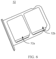
- FIG. 6 is a schematic structural diagram of a card tray in an embodiment of a mobile device according to this application.
- a card tray 52 includes a first card slot 52a and a second card slot 52b, and a shape of the first card slot 52a is the same as that of the second card slot 52b.
- the first card slot 52a and the second card slot 52b are configured to accommodate a plurality of types of memory cards provided in the foregoing embodiment.
- the mobile device may be a wearable device such as a mobile phone, a tablet computer, or a smartwatch.
- the mobile device may further include a memory, configured to store program data.
- the program data is executed by the controller 51, the foregoing identification method is implemented.
- the method may be stored in a computer-readable storage medium.
- the computer software product is stored in a storage medium and includes several instructions for instructing a computer device (which may be a personal computer, a server, or a network device) or a processor to perform all or some of the steps of the methods described in the implementations of this application.
- the foregoing storage medium includes: any medium that can store program code, such as a USB flash drive, a removable hard disk, a read-only memory (ROM, Read-Only Memory), a random access memory (RAM, Random Access Memory), a magnetic disk, or an optical disc.
- program code such as a USB flash drive, a removable hard disk, a read-only memory (ROM, Read-Only Memory), a random access memory (RAM, Random Access Memory), a magnetic disk, or an optical disc.
Landscapes
- Engineering & Computer Science (AREA)
- Theoretical Computer Science (AREA)
- Physics & Mathematics (AREA)
- General Physics & Mathematics (AREA)
- Computer Hardware Design (AREA)
- Microelectronics & Electronic Packaging (AREA)
- General Engineering & Computer Science (AREA)
- Artificial Intelligence (AREA)
- Computer Vision & Pattern Recognition (AREA)
- Telephone Function (AREA)
- Telephonic Communication Services (AREA)
- Power Sources (AREA)
- Techniques For Improving Reliability Of Storages (AREA)
Claims (13)
- Procédé d'identification de carte mémoire, dans lequel le procédé comprend :l'envoi (11, 21, 32, 42) d'une commande d'initialisation d'un protocole de communication de carte mémoire de premier type à une carte mémoire à identifier ;le fait de détecter (12, 22, 33, 43) s'il y a une réponse ; etl'identification (13, 23, 24, 34, 35, 44, 45) de la carte mémoire ;caractérisé en ce quela réponse est une réponse sur une broche de commande de la carte mémoire et la carte mémoire est identifiée comme une carte mémoire de premier type ou une carte mémoire de second type sur la base d'un état de réponse de la broche de commande ;le procédé comprenant en outreavant l'étape d'envoi d'une commande d'initialisation d'un protocole de communication de carte mémoire de premier type vers une carte mémoire à identifier :
la mise sous tension d'une broche DAT3 de la carte mémoire à identifier, de sorte que la broche DAT3 est dans un état non mis à la terre. - Procédé selon la revendication 1, dans lequel
l'identification de la carte mémoire en tant que carte mémoire de premier type ou carte mémoire de second type sur la base d'un état de réponse de la broche de commande comprend :l'identification (23, 34, 44) de la carte mémoire comme carte mémoire de premier type s'il y a une réponse ; oul'identification (24, 35, 45) de la carte mémoire comme carte mémoire de second type en cas d'absence de réponse. - Procédé selon la revendication 2, dans lequel
après l'étape d'identification de la carte mémoire comme carte mémoire de premier type, le procédé comprend en outre :
l'initialisation de la carte mémoire de premier type à l'aide de la commande d'initialisation du protocole de communication de carte mémoire de premier type. - Procédé selon la revendication 2, dans lequel
après l'étape d'identification de la carte mémoire comme carte mémoire de second type, le procédé comprend en outre :
l'initialisation de la carte mémoire de second type à l'aide d'une commande d'initialisation d'un protocole de communication de carte mémoire de second type. - Procédé selon l'une quelconque des revendications 1 à 4, dans lequel
avant l'étape d'envoi d'une commande d'initialisation d'un protocole de communication de carte mémoire de premier type vers une carte mémoire à identifier, le procédé comprend en outre :
l'envoi (31) d'une commande de réinitialisation partagée par le protocole de communication de la carte mémoire du premier type et le protocole de communication de la carte mémoire du second type à la broche de commande de la carte mémoire à identifier, de sorte que la carte mémoire à identifier entre dans un état inactif. - Procédé selon l'une quelconque des revendications 1 à 5, dans lequel
la carte mémoire du premier type est une carte MMC, et la carte mémoire du second type est une carte SD. - Procédé selon la revendication 5 ou 6 lorsqu'elle dépend de la revendication 5, dans lequel la commande de réinitialisation est une commande CMD0.
- Procédé selon l'une quelconque des revendications 1 à 7, dans lequel
avant l'étape d'envoi d'une commande d'initialisation d'un protocole de communication de carte mémoire de premier type vers une carte mémoire à identifier, le procédé comprend en outre :
la mise sous tension (41) de la carte mémoire. - Procédé selon l'une quelconque des revendications 1 à 8, dans lequel
la commande d'initialisation est une commande CMD1. - Procédé selon la revendication 8, dans lequel la mise sous tension de la carte mémoire comprend la mise sous tension de la carte mémoire à l'aide d'une tension de 3,3 V.
- Dispositif mobile (50), dans lequel le dispositif mobile comprend un dispositif de commande (51) et un plateau de carte (52) qui peut être intégré dans un corps du dispositif mobile (50), un logement pour carte est disposé sur le plateau de carte (52), le logement pour carte (52a) est conçu pour recevoir une carte mémoire et connecter électriquement la carte mémoire et le dispositif de commande (51), et le dispositif de commande (51) est configuré pour identifier la carte mémoire à l'aide du procédé selon l'une quelconque des revendications 1 à 8.
- Dispositif mobile selon la revendication 11, dans lequel le dispositif mobile est un téléphone mobile, une tablette électronique ou une montre intelligente.
- Dispositif mobile selon la revendication 11 ou 12, dans lequel le plateau de carte (52) du dispositif mobile (50) comprend un premier logement pour carte (52a) et un second logement pour carte (52b), une forme du premier logement pour carte (52a) étant la même qu'une forme du second logement pour carte (52b).
Applications Claiming Priority (2)
| Application Number | Priority Date | Filing Date | Title |
|---|---|---|---|
| CN201811585279.9A CN111428842B (zh) | 2018-12-24 | 2018-12-24 | 一种存储卡的识别方法以及移动设备 |
| PCT/CN2019/096438 WO2020134040A1 (fr) | 2018-12-24 | 2019-07-17 | Procédé d'identification de carte mémoire et dispositif mobile |
Publications (4)
| Publication Number | Publication Date |
|---|---|
| EP3876154A1 EP3876154A1 (fr) | 2021-09-08 |
| EP3876154A4 EP3876154A4 (fr) | 2022-01-05 |
| EP3876154B1 true EP3876154B1 (fr) | 2023-09-06 |
| EP3876154C0 EP3876154C0 (fr) | 2023-09-06 |
Family
ID=71129051
Family Applications (1)
| Application Number | Title | Priority Date | Filing Date |
|---|---|---|---|
| EP19903739.1A Active EP3876154B1 (fr) | 2018-12-24 | 2019-07-17 | Procédé d'identification de carte mémoire et dispositif mobile |
Country Status (5)
| Country | Link |
|---|---|
| US (1) | US11893436B2 (fr) |
| EP (1) | EP3876154B1 (fr) |
| CN (1) | CN111428842B (fr) |
| ES (1) | ES2960711T3 (fr) |
| WO (1) | WO2020134040A1 (fr) |
Families Citing this family (2)
| Publication number | Priority date | Publication date | Assignee | Title |
|---|---|---|---|---|
| CN111414125A (zh) * | 2018-12-18 | 2020-07-14 | 华为技术有限公司 | 一种存储设备的操作方法及存储设备 |
| CN112820345A (zh) * | 2020-12-31 | 2021-05-18 | 展讯通信(上海)有限公司 | 存储卡兼容性测试方法及系统 |
Family Cites Families (24)
| Publication number | Priority date | Publication date | Assignee | Title |
|---|---|---|---|---|
| US6438638B1 (en) * | 2000-07-06 | 2002-08-20 | Onspec Electronic, Inc. | Flashtoaster for reading several types of flash-memory cards with or without a PC |
| US6725291B2 (en) * | 2002-01-18 | 2004-04-20 | Key Technology Corporation | Detection method used in adaptor capable of inserting various kinds of memory cards |
| US7225357B2 (en) * | 2003-01-21 | 2007-05-29 | Zentek Technology Japan, Inc. | SDIO card development system |
| US7069369B2 (en) | 2004-02-12 | 2006-06-27 | Super Talent Electronics, Inc. | Extended-Secure-Digital interface using a second protocol for faster transfers |
| TWI271659B (en) | 2004-05-05 | 2007-01-21 | Prolific Technology Inc | Memory card equipped with a multi-interface function and method for choosing a compatible transmission mode |
| JP4209820B2 (ja) * | 2004-07-15 | 2009-01-14 | 株式会社ハギワラシスコム | メモリカードシステム及び該メモリカードシステムで使用されるライトワンス型メモリカード、ホストシステムと半導体記憶デバイスとからなるシステム |
| US20060218324A1 (en) * | 2005-03-25 | 2006-09-28 | Matsushita Electrical Industrial Co., Ltd | Systems and methods for flexible data transfers in SDIO and/or MMC |
| US7739487B2 (en) * | 2006-01-17 | 2010-06-15 | Nokia Corporation | Method for booting a host device from an MMC/SD device, a host device bootable from an MMC/SD device and an MMC/SD device method a host device may booted from |
| US20070274033A1 (en) * | 2006-05-26 | 2007-11-29 | Chin-Hwa Hwang | Drawer-type memory card adapter |
| KR100782113B1 (ko) * | 2006-11-13 | 2007-12-05 | 삼성전자주식회사 | 메모리 카드 시스템 및 그것의 호스트 식별 정보 전송 방법 |
| CN101483939B (zh) * | 2008-01-09 | 2012-04-25 | 联芯科技有限公司 | 一种识别终端卡的方法及装置 |
| US20100125689A1 (en) | 2008-11-20 | 2010-05-20 | Mediatek Inc. | Electronic apparatus capable of receiving different types of memory cards |
| US7899967B2 (en) * | 2008-11-24 | 2011-03-01 | Mediatek Inc. | Systems for accessing memory card and methods for accessing memory card by a control unit |
| US20100224684A1 (en) * | 2009-03-03 | 2010-09-09 | Atmel Corporation | Smart card reader |
| CN102253809A (zh) * | 2010-05-17 | 2011-11-23 | 中兴通讯股份有限公司 | 一种复合存储卡及其控制方法 |
| CN101986327A (zh) * | 2010-09-06 | 2011-03-16 | 建荣集成电路科技(珠海)有限公司 | 一种sd/mmc卡免检测脚在线/离线检测方法 |
| US8621258B2 (en) * | 2011-07-18 | 2013-12-31 | Maishi Electronic (Shanghai) Ltd. | Device for operating two memory cards in two sockets with different pin arrangements |
| EP2849119A4 (fr) * | 2012-05-08 | 2015-04-29 | Panasonic Corp | Unité de dispositif, dispositif d'accès, système d'accès et procédé d'établissement de communication |
| CN103310175B (zh) * | 2013-06-24 | 2016-01-20 | 飞天诚信科技股份有限公司 | 一种基于标准ccid协议的多卡槽读卡器的工作方法 |
| KR20160045284A (ko) * | 2014-10-17 | 2016-04-27 | 삼성전자주식회사 | 트레이, 트레이 분리용 지그 및 그것을 포함하는 전자 장치 |
| EP3197059B1 (fr) * | 2016-01-21 | 2018-07-18 | Samsung Electronics Co., Ltd | Procédé de contrôle de carte sim et de carte sd et dispositif électronique mettant en oeuvre ledit procédé |
| CN106776383B (zh) * | 2016-12-28 | 2023-07-04 | 深圳市道通智能航空技术股份有限公司 | 存储卡的识别方法、装置及电子设备 |
| US10353840B2 (en) * | 2017-11-27 | 2019-07-16 | Motorola Solutions, Inc. | Secure digital format card having two interfaces to communicate with two processors |
| US10296766B2 (en) * | 2018-01-11 | 2019-05-21 | Intel Corporation | Technologies for secure enumeration of USB devices |
-
2018
- 2018-12-24 CN CN201811585279.9A patent/CN111428842B/zh active Active
-
2019
- 2019-07-17 ES ES19903739T patent/ES2960711T3/es active Active
- 2019-07-17 US US17/417,705 patent/US11893436B2/en active Active
- 2019-07-17 WO PCT/CN2019/096438 patent/WO2020134040A1/fr not_active Ceased
- 2019-07-17 EP EP19903739.1A patent/EP3876154B1/fr active Active
Also Published As
| Publication number | Publication date |
|---|---|
| EP3876154A4 (fr) | 2022-01-05 |
| ES2960711T3 (es) | 2024-03-06 |
| CN111428842A (zh) | 2020-07-17 |
| US20220076090A1 (en) | 2022-03-10 |
| CN111428842B (zh) | 2022-10-18 |
| EP3876154A1 (fr) | 2021-09-08 |
| WO2020134040A1 (fr) | 2020-07-02 |
| EP3876154C0 (fr) | 2023-09-06 |
| US11893436B2 (en) | 2024-02-06 |
Similar Documents
| Publication | Publication Date | Title |
|---|---|---|
| CN100507940C (zh) | 可移除电子电路卡的模块之间的有效连接 | |
| US7836236B2 (en) | Extended secure-digital (SD) devices and hosts | |
| EP2128789B1 (fr) | Procédé pour réduire l'interférence RF dans un lecteur à double interface de cartes et lecteur à double interface correspondant | |
| JP7200366B2 (ja) | メモリカード、メモリカードアダプタ、及び端末デバイス | |
| US20040064612A1 (en) | Method and system for using a memory card protocol inside a bus protocol | |
| KR101754438B1 (ko) | 페이징된 낸드 파워-온 리셋 | |
| US10360490B2 (en) | IC card, portable terminal, and portable electronic apparatus | |
| EP3876154A1 (fr) | Procédé d'identification de carte mémoire et dispositif mobile | |
| EP2911066B1 (fr) | Procédé de transfert de données, dispositif de programme informatique et étiquette | |
| CN101221547B (zh) | 具有多个接口的存储卡及其复位控制方法 | |
| CN111414125A (zh) | 一种存储设备的操作方法及存储设备 | |
| CN100373404C (zh) | 一种初始化存储卡的方法 | |
| CN111428841B (zh) | 一种存储卡的识别方法以及移动设备 | |
| CN111428840B (zh) | 一种功能卡的识别方法以及移动设备 | |
| US9251454B2 (en) | Storage medium, transmittal system and control method thereof | |
| CN111428526B (zh) | 一种功能卡的识别方法以及移动设备 |
Legal Events
| Date | Code | Title | Description |
|---|---|---|---|
| STAA | Information on the status of an ep patent application or granted ep patent |
Free format text: STATUS: THE INTERNATIONAL PUBLICATION HAS BEEN MADE |
|
| PUAI | Public reference made under article 153(3) epc to a published international application that has entered the european phase |
Free format text: ORIGINAL CODE: 0009012 |
|
| STAA | Information on the status of an ep patent application or granted ep patent |
Free format text: STATUS: REQUEST FOR EXAMINATION WAS MADE |
|
| 17P | Request for examination filed |
Effective date: 20210604 |
|
| AK | Designated contracting states |
Kind code of ref document: A1 Designated state(s): AL AT BE BG CH CY CZ DE DK EE ES FI FR GB GR HR HU IE IS IT LI LT LU LV MC MK MT NL NO PL PT RO RS SE SI SK SM TR |
|
| A4 | Supplementary search report drawn up and despatched |
Effective date: 20211206 |
|
| RIC1 | Information provided on ipc code assigned before grant |
Ipc: G06F 13/38 20060101ALI20211130BHEP Ipc: G06K 19/077 20060101ALI20211130BHEP Ipc: G06K 7/00 20060101ALI20211130BHEP Ipc: G06K 19/07 20060101AFI20211130BHEP |
|
| DAV | Request for validation of the european patent (deleted) | ||
| DAX | Request for extension of the european patent (deleted) | ||
| GRAP | Despatch of communication of intention to grant a patent |
Free format text: ORIGINAL CODE: EPIDOSNIGR1 |
|
| STAA | Information on the status of an ep patent application or granted ep patent |
Free format text: STATUS: GRANT OF PATENT IS INTENDED |
|
| INTG | Intention to grant announced |
Effective date: 20230203 |
|
| GRAS | Grant fee paid |
Free format text: ORIGINAL CODE: EPIDOSNIGR3 |
|
| GRAA | (expected) grant |
Free format text: ORIGINAL CODE: 0009210 |
|
| STAA | Information on the status of an ep patent application or granted ep patent |
Free format text: STATUS: THE PATENT HAS BEEN GRANTED |
|
| AK | Designated contracting states |
Kind code of ref document: B1 Designated state(s): AL AT BE BG CH CY CZ DE DK EE ES FI FR GB GR HR HU IE IS IT LI LT LU LV MC MK MT NL NO PL PT RO RS SE SI SK SM TR |
|
| REG | Reference to a national code |
Ref country code: GB Ref legal event code: FG4D |
|
| REG | Reference to a national code |
Ref country code: CH Ref legal event code: EP |
|
| REG | Reference to a national code |
Ref country code: IE Ref legal event code: FG4D |
|
| REG | Reference to a national code |
Ref country code: DE Ref legal event code: R096 Ref document number: 602019037150 Country of ref document: DE |
|
| U01 | Request for unitary effect filed |
Effective date: 20230906 |
|
| U07 | Unitary effect registered |
Designated state(s): AT BE BG DE DK EE FI FR IT LT LU LV MT NL PT SE SI Effective date: 20230912 |
|
| PG25 | Lapsed in a contracting state [announced via postgrant information from national office to epo] |
Ref country code: GR Free format text: LAPSE BECAUSE OF FAILURE TO SUBMIT A TRANSLATION OF THE DESCRIPTION OR TO PAY THE FEE WITHIN THE PRESCRIBED TIME-LIMIT Effective date: 20231207 |
|
| PG25 | Lapsed in a contracting state [announced via postgrant information from national office to epo] |
Ref country code: RS Free format text: LAPSE BECAUSE OF FAILURE TO SUBMIT A TRANSLATION OF THE DESCRIPTION OR TO PAY THE FEE WITHIN THE PRESCRIBED TIME-LIMIT Effective date: 20230906 Ref country code: NO Free format text: LAPSE BECAUSE OF FAILURE TO SUBMIT A TRANSLATION OF THE DESCRIPTION OR TO PAY THE FEE WITHIN THE PRESCRIBED TIME-LIMIT Effective date: 20231206 Ref country code: HR Free format text: LAPSE BECAUSE OF FAILURE TO SUBMIT A TRANSLATION OF THE DESCRIPTION OR TO PAY THE FEE WITHIN THE PRESCRIBED TIME-LIMIT Effective date: 20230906 Ref country code: GR Free format text: LAPSE BECAUSE OF FAILURE TO SUBMIT A TRANSLATION OF THE DESCRIPTION OR TO PAY THE FEE WITHIN THE PRESCRIBED TIME-LIMIT Effective date: 20231207 |
|
| REG | Reference to a national code |
Ref country code: ES Ref legal event code: FG2A Ref document number: 2960711 Country of ref document: ES Kind code of ref document: T3 Effective date: 20240306 |
|
| PG25 | Lapsed in a contracting state [announced via postgrant information from national office to epo] |
Ref country code: IS Free format text: LAPSE BECAUSE OF FAILURE TO SUBMIT A TRANSLATION OF THE DESCRIPTION OR TO PAY THE FEE WITHIN THE PRESCRIBED TIME-LIMIT Effective date: 20240106 |
|
| PG25 | Lapsed in a contracting state [announced via postgrant information from national office to epo] |
Ref country code: SM Free format text: LAPSE BECAUSE OF FAILURE TO SUBMIT A TRANSLATION OF THE DESCRIPTION OR TO PAY THE FEE WITHIN THE PRESCRIBED TIME-LIMIT Effective date: 20230906 Ref country code: RO Free format text: LAPSE BECAUSE OF FAILURE TO SUBMIT A TRANSLATION OF THE DESCRIPTION OR TO PAY THE FEE WITHIN THE PRESCRIBED TIME-LIMIT Effective date: 20230906 Ref country code: IS Free format text: LAPSE BECAUSE OF FAILURE TO SUBMIT A TRANSLATION OF THE DESCRIPTION OR TO PAY THE FEE WITHIN THE PRESCRIBED TIME-LIMIT Effective date: 20240106 Ref country code: CZ Free format text: LAPSE BECAUSE OF FAILURE TO SUBMIT A TRANSLATION OF THE DESCRIPTION OR TO PAY THE FEE WITHIN THE PRESCRIBED TIME-LIMIT Effective date: 20230906 Ref country code: SK Free format text: LAPSE BECAUSE OF FAILURE TO SUBMIT A TRANSLATION OF THE DESCRIPTION OR TO PAY THE FEE WITHIN THE PRESCRIBED TIME-LIMIT Effective date: 20230906 |
|
| PG25 | Lapsed in a contracting state [announced via postgrant information from national office to epo] |
Ref country code: PL Free format text: LAPSE BECAUSE OF FAILURE TO SUBMIT A TRANSLATION OF THE DESCRIPTION OR TO PAY THE FEE WITHIN THE PRESCRIBED TIME-LIMIT Effective date: 20230906 |
|
| REG | Reference to a national code |
Ref country code: DE Ref legal event code: R097 Ref document number: 602019037150 Country of ref document: DE |
|
| PLBE | No opposition filed within time limit |
Free format text: ORIGINAL CODE: 0009261 |
|
| STAA | Information on the status of an ep patent application or granted ep patent |
Free format text: STATUS: NO OPPOSITION FILED WITHIN TIME LIMIT |
|
| 26N | No opposition filed |
Effective date: 20240607 |
|
| U20 | Renewal fee for the european patent with unitary effect paid |
Year of fee payment: 6 Effective date: 20240731 |
|
| PG25 | Lapsed in a contracting state [announced via postgrant information from national office to epo] |
Ref country code: MC Free format text: LAPSE BECAUSE OF FAILURE TO SUBMIT A TRANSLATION OF THE DESCRIPTION OR TO PAY THE FEE WITHIN THE PRESCRIBED TIME-LIMIT Effective date: 20230906 |
|
| REG | Reference to a national code |
Ref country code: CH Ref legal event code: PL |
|
| PG25 | Lapsed in a contracting state [announced via postgrant information from national office to epo] |
Ref country code: CH Free format text: LAPSE BECAUSE OF NON-PAYMENT OF DUE FEES Effective date: 20240731 |
|
| PGFP | Annual fee paid to national office [announced via postgrant information from national office to epo] |
Ref country code: GB Payment date: 20250529 Year of fee payment: 7 |
|
| PG25 | Lapsed in a contracting state [announced via postgrant information from national office to epo] |
Ref country code: IE Free format text: LAPSE BECAUSE OF NON-PAYMENT OF DUE FEES Effective date: 20240717 |
|
| U20 | Renewal fee for the european patent with unitary effect paid |
Year of fee payment: 7 Effective date: 20250731 |
|
| PGFP | Annual fee paid to national office [announced via postgrant information from national office to epo] |
Ref country code: ES Payment date: 20250806 Year of fee payment: 7 |
|
| PG25 | Lapsed in a contracting state [announced via postgrant information from national office to epo] |
Ref country code: CY Free format text: LAPSE BECAUSE OF FAILURE TO SUBMIT A TRANSLATION OF THE DESCRIPTION OR TO PAY THE FEE WITHIN THE PRESCRIBED TIME-LIMIT; INVALID AB INITIO Effective date: 20190717 |
|
| PG25 | Lapsed in a contracting state [announced via postgrant information from national office to epo] |
Ref country code: HU Free format text: LAPSE BECAUSE OF FAILURE TO SUBMIT A TRANSLATION OF THE DESCRIPTION OR TO PAY THE FEE WITHIN THE PRESCRIBED TIME-LIMIT; INVALID AB INITIO Effective date: 20190717 |