EP3876251A1 - Empilement sans fil comprenant des condensateurs céramiques - Google Patents
Empilement sans fil comprenant des condensateurs céramiques Download PDFInfo
- Publication number
- EP3876251A1 EP3876251A1 EP21160086.1A EP21160086A EP3876251A1 EP 3876251 A1 EP3876251 A1 EP 3876251A1 EP 21160086 A EP21160086 A EP 21160086A EP 3876251 A1 EP3876251 A1 EP 3876251A1
- Authority
- EP
- European Patent Office
- Prior art keywords
- ceramic capacitor
- capacitor
- multilayer ceramic
- conductive adhesive
- electroplating
- Prior art date
- Legal status (The legal status is an assumption and is not a legal conclusion. Google has not performed a legal analysis and makes no representation as to the accuracy of the status listed.)
- Pending
Links
Images




Classifications
-
- H—ELECTRICITY
- H01—ELECTRIC ELEMENTS
- H01G—CAPACITORS; CAPACITORS, RECTIFIERS, DETECTORS, SWITCHING DEVICES, LIGHT-SENSITIVE OR TEMPERATURE-SENSITIVE DEVICES OF THE ELECTROLYTIC TYPE
- H01G2/00—Details of capacitors not covered by a single one of groups H01G4/00-H01G11/00
- H01G2/02—Mountings
- H01G2/06—Mountings specially adapted for mounting on a printed-circuit support
- H01G2/065—Mountings specially adapted for mounting on a printed-circuit support for surface mounting, e.g. chip capacitors
-
- H—ELECTRICITY
- H01—ELECTRIC ELEMENTS
- H01G—CAPACITORS; CAPACITORS, RECTIFIERS, DETECTORS, SWITCHING DEVICES, LIGHT-SENSITIVE OR TEMPERATURE-SENSITIVE DEVICES OF THE ELECTROLYTIC TYPE
- H01G4/00—Fixed capacitors; Processes of their manufacture
- H01G4/30—Stacked capacitors
-
- H—ELECTRICITY
- H01—ELECTRIC ELEMENTS
- H01G—CAPACITORS; CAPACITORS, RECTIFIERS, DETECTORS, SWITCHING DEVICES, LIGHT-SENSITIVE OR TEMPERATURE-SENSITIVE DEVICES OF THE ELECTROLYTIC TYPE
- H01G4/00—Fixed capacitors; Processes of their manufacture
- H01G4/002—Details
- H01G4/018—Dielectrics
- H01G4/06—Solid dielectrics
- H01G4/08—Inorganic dielectrics
- H01G4/12—Ceramic dielectrics
-
- H—ELECTRICITY
- H01—ELECTRIC ELEMENTS
- H01G—CAPACITORS; CAPACITORS, RECTIFIERS, DETECTORS, SWITCHING DEVICES, LIGHT-SENSITIVE OR TEMPERATURE-SENSITIVE DEVICES OF THE ELECTROLYTIC TYPE
- H01G4/00—Fixed capacitors; Processes of their manufacture
- H01G4/002—Details
- H01G4/228—Terminals
- H01G4/232—Terminals electrically connecting two or more layers of a stacked or rolled capacitor
-
- H—ELECTRICITY
- H01—ELECTRIC ELEMENTS
- H01G—CAPACITORS; CAPACITORS, RECTIFIERS, DETECTORS, SWITCHING DEVICES, LIGHT-SENSITIVE OR TEMPERATURE-SENSITIVE DEVICES OF THE ELECTROLYTIC TYPE
- H01G4/00—Fixed capacitors; Processes of their manufacture
- H01G4/38—Multiple capacitors, i.e. structural combinations of fixed capacitors
- H01G4/385—Single unit multiple capacitors, e.g. dual capacitor in one coil
Definitions
- the present invention relates to ceramic capacitor technology and more particularly, to a leadless stack comprising ceramic capacitor, especially the external electrodes of a plurality of stacked ceramic capacitors are adhered and fixed by conductive adhesive.
- the multi-layer ceramic capacitor (MLCC) in ceramic capacitors its capacitance content is proportional to the surface area of the product and the number of layers of ceramic film stacked, and the MLCC can be directly adhered through the surface mount technology (SMT) process, and the production speed is faster. Coupled with its advantages such as easy chipization, small size and good frequency characteristics, the MLCC has become a mainstream product in the capacitor industry.
- the disadvantage of the MLCC is that the capacitance value is small.
- the conventional multilayer ceramic capacitor stack is to form a junction point of the two sides of the external electrode A1 of the multilayer ceramic capacitor A through solder B , and weld it to the junction surface C1 on the opposite inner side of the two lead frames C to form a stacked structure, and then welded on the circuit board by the outer leads C2 of the lead frames C .
- the two lead frames C can provide support strength and conductive channels at the same time, so that the total capacitance value can be improved.
- the temperature required for the welding process is mostly higher than 300°C.
- TLPS transient-liquid-phase-sintering
- the solder used at the same time, and form a stacked junction on the outer electrode end of each ceramic capacitor, so that multiple ceramic capacitors are stacked and supported each other like building blocks without collapsing. Moreover, the junction also forms a conductive path. Since the lead frame is not used for mounting, it must be able to resist the stress damage caused by the bending of the substrate, and it cannot even cause an unexpected degree of stress damage to the ceramic capacitor stacking position or the junction.
- TLPS paste as a bonding material needs to rely on high temperature heating to easily form intermetallic compounds. Although it has the advantage of improving mechanical strength, high temperature heating and phase change processes will increase process variation factors. If you observe the microstructure of the sintered joints, it is easy to form hard and brittle intermetallic compounds, and even the stacking position or the surface of the bonding point forms microcracks after phase change or volume change. Even if the support strength is sufficient, it still cannot effectively provide the toughness that can resist the repeated bending or vibration of the plate. On the contrary, it will promote the stress concentration to form a source of structural damage or rupture, which limits the application of the product.
- TLPS paste cannot be filled with nickel or tin plating after sintering, it is difficult to react with the electroplating solution to form a uniform and detailed electroplating surface. Therefore, the problem of micro cracks or micro gaps cannot be improved. This industry is eager to study the direction of improvement.
- the present invention has been accomplished under the circumstances in view. It is a first object of the present invention to provide a leadless stack comprising ceramic capacitor, which lets the external electrodes of a plurality of multilayer ceramic capacitors use a polymer conductive adhesive as the bonding material to form a adhesive interface that provides support strength and conductive channels, so that the external electrodes of the multiple multilayer ceramic capacitors can be stacked vertically with each other through the adhesive interface to be electrically conductive and form a series combination. Its total capacitance value is also proportional to the number of capacitors stacked.
- the polymer conductive adhesive contains 75% ⁇ 85% metal powder and 15% ⁇ 25% viscose, which can make the adhesive interface have sufficient supporting adhesion strength, and the toughness required to absorb the bending or vibration energy of the board, and resist the bending of the repeated board or mechanical damage caused by the vibrating environment. This can eliminate the need for high-temperature heating of metal leads and TLPS paste, simplifying the process, and the operating temperature of the solderless operation of the polymer conductive adhesive is relatively low, and the process variation factors are relatively reduced.
- the secondary object of the present invention is that the adhesive interface of the stacking position of a plurality of multilayer ceramic capacitors with external electrodes between each other can be electroplated, and a first plating layer and a second plating layer of an electroplating strengthening layer are formed by nickel plating and tin plating in sequence. Since the polymer conductive adhesive used in the adhesive interface contains sufficient metal powder, it can react with the electroplating solution to form a uniform and detailed electroplating surface, so that any micro cracks or micro gaps on the adhesive interface will be filled by the electroplating strengthening layer after electroplating to avoid the formation of cracked nuclei.
- each adhesive interface and the external electrodes of the multilayer ceramic capacitors can form the flat side surface of the electroplating strengthening layer, so that the electroplating strengthening layer can completely cover the external electrodes of the multiple multilayer ceramic capacitors, thereby strengthening the mechanical strength of the adhesive interface.
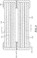
- the leadless stack comprising ceramic capacitor comprises a plurality of multilayer ceramic capacitors 100 stacked vertically to each other, wherein each multilayer ceramic capacitor 100 comprises a capacitor body 110 , a plurality of dielectric layers 111 stacked in each capacitor body 110 , a plurality of internal electrodes 120 interspersed in each two adjacent dielectric layers 111 and arranged facing each other in a staggered manner with electrode ends thereof respectively exposed to two opposite ends of the capacitor body 110 , and two external electrodes 130 respectively arranged on the two ends of the capacitor body 110 and electrically connected to the ends of the internal electrodes 120 .
- the external electrode 130 is the innermost layer of the external electrode formed by burning copper or called burning copper layer.
- the external electrodes 130 of each two adjacent multilayer ceramic capacitors 100 are bonded and fixed in a temperature range of 150°C to 200°C through a polymer conductive adhesive 210 to form a adhesive interface 200 at each end without welding.
- two multilayer ceramic capacitors 100 are vertically stacked up and down, and the external electrodes 130 of the two multilayer ceramic capacitors 100 are adhered and fixed to each other through the polymer conductive adhesive 210 to form the adhesive interface 200 .
- the overall structure is a stack of multiple multilayer ceramic capacitors 100 .
- the stacking method is to first apply the polymer conductive adhesive 210 to the upper surface of the external electrodes 130 of the first multilayer ceramic capacitor 100 , and to attach the lower surface of the external electrodes 130 of the second multilayer ceramic capacitor 100 to the polymer conductive adhesive 210 .
- the conductive adhesive 210 On the conductive adhesive 210 , at the same time, make the burnt copper of the external electrodes 130 of the second multilayer ceramic capacitor 100 correspond to the burnt copper of the external electrodes 130 of the first multilayer ceramic capacitor 100 and stack them on the same position, and then proceed low temperature operation about 150 ⁇ 200°C temperature range without welding. After the polymer conductive adhesive 210 is cured, the two adjacent external electrodes 130 can be adhered and fixed to form the adhesive interface 200 with support strength and as a conductive channel for the two adjacent external electrodes 130 , so that two multilayer ceramic capacitors 100 can be electrically conducted to form a series combination. Its total capacitance value is higher than that of a single multilayer ceramic capacitor 100 , and because the capacitor stack structure does not need to be heated at high temperature to form a bond, in addition to less process variation factors, the damage to the capacitor body can also be minimized.
- the external electrodes 130 of the plurality of multilayer ceramic capacitors 100 are bonded to each other using polymer conductive adhesive 210 as the bonding material, and after curing, the adhesive interface 200 can be formed to provide support strength and conductive channels.
- the composition of polymer conductive adhesive 210 comprises 75% ⁇ 85% of metal powder and 15% ⁇ 25% of viscose, wherein the metal powder is selected from the group consisting of silver (Ag), copper (Cu) and nickel (Ni), and the adhesive uses a polymer resin, and has a special viscous strength.
- the better specification is the polymer conductive adhesive of H926 commercially available product specification, such as resin silver glue, and the suitable ratio can also be adjusted according to different requirements of polymer (generally called polymer) resin, fluidity or conductivity, etc. , or can adjust the suitable ratio according to the specifications of different models of multilayer ceramic capacitor 100 and the number of stacks.
- the polymer resin can contain 75% to 85% of the metal powder without affecting the purpose of the present invention, but it is not limited to this.
- Graphene can also be added to the polymer resin, and the metal powder and graphene can be further adjusted.
- the suitable ratio of different compositions of polymer resin makes the polymer conductive adhesive 210 more excellent in conductivity.
- the adhesive interface 200 formed by the resin silver glue has the strong and tough characteristics of a polymer material, and after the resin is cured, it can provide sufficient adhesion strength to support the capacitor stack structure. Moreover, the polymer components contained in the resin can give the toughness required to absorb the bending or vibration energy of the board, and it can effectively resist the mechanical damage caused by the repeated bending of the board or the vibration environment.
- the number of multilayer ceramic capacitors 100 that can be stacked in the above-mentioned capacitor stack structure is not fixed, and two or more can be stacked according to the specifications (such as volume and weight) of different types of multilayer ceramic capacitors 100 . The preferred implementation is between two to four, and the adhesive interface 200 can still provide sufficient support strength without collapse.
- the composition of the polymer conductive adhesive 210 used in the adhesive interface 200 can be adjusted according to different multilayer ceramic capacitors 100 and the number of stacks.
- the selected metal powder particle size can also be between 0.3 and 5.0 ⁇ m.
- the closer the multilayer ceramic capacitor 100 to the bottom side the greater the load.
- the external electrodes 130 where the multiple multilayer ceramic capacitors 100 are stacked are applied with a polymer conductive adhesive 210 to form the adhesive interface 200 .
- the outside of each adhesive interface 200 can be electroplated to form a first plating layer 221 and a second plating layer 222 of an electroplating strengthening layer 220 with nickel plating and tin plating in sequence.
- the polymer conductive adhesive 210 contains 75% ⁇ 85% of sufficient metal powder, it can react with the electroplating solution to form a uniform and detailed electroplating surface, so that any micro cracks or micro gaps on the adhesive interface 200 will be filled by the electroplating strengthening layer 220 after electroplating to avoid the formation of cracked nuclei.
- each adhesive interface 200 and the external electrodes 130 of the multilayer ceramic capacitors 100 co-extend each adhesive interface 200 and the external electrodes 130 of the multilayer ceramic capacitors 100 to form the flat side surface of the electroplating strengthening layer 220 , so that the electroplating strengthening layer 220 can completely cover the external electrodes 130 of the multiple multilayer ceramic capacitors 100 , thereby strengthening the mechanical strength of the adhesive interface 200 .
- the external electrodes 130 at one end of multiple multilayer ceramic capacitors 100 or multiple burnt copper layers can be covered by the same continuous and uninterrupted surface electroplating strengthening layer 220 , so as to form a special external terminal electrode that can achieve the effect of multiple ceramic capacitors in series at the same time.
- the electroplating strengthening layer 220 covers the external electrodes 130 of vertically stacked multilayer ceramic capacitors 100 that use polymer conductive adhesive 210 to form the adhesive interface 200 .
- This type of leadless stack comprising ceramic capacitor can eliminate the use of metal leads and the troubles and limitations of high-temperature heating of TLPS paste as a bonding material.
- the curing temperature of the polymer conductive adhesive 210 without soldering is relatively low, so that the process variation factors are relatively reduced, so as to achieve the purpose of improving product yield and reducing costs.
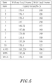
- FIG. 5-6 can be learned from the data table of the leadless stack comprising ceramic capacitor (without lead frame) of the present invention and the conventional multilayer ceramic capacitor (with lead frame) as the comparison group for the side push experiment.
- the average lateral thrust (AVG) measured in the comparison group was approximately 166.7N. f.
- the range of the minimum (MIN) and maximum (MAX) lateral thrust is between 120 ⁇ 180N. f, it is the mechanical strength level of the multilayer ceramic capacitors with lead frame on the market. Specifically, even if the leadless stack comprising ceramic capacitor of the experimental group of the present invention removes the metal leads (without lead frame), the actual measured average lateral thrust (AVG) is about 165.228N.
- the range of the minimum (MIN) and maximum (MAX) lateral thrust is between 133.28-176.4N. f.
- the overall lateral strength value performance is not inferior to multilayer ceramic capacitors with metal leads, but the production process is far more simplified than the comparison group above. Even if metal leads are not used for surface mounting (SMT) on the circuit board, it still has the toughness required to absorb the bending or vibration energy of the board, and will not cause unpredictable levels of stress in the stacking position of the multilayer ceramic capacitors 100 or the adhesive interface 200 damage, it can effectively resist mechanical damage caused by repeated plate bending or vibration environment.
- SMT surface mounting
- the leadless stack comprising ceramic capacitor of the experimental group of the present invention
- its manufacturing process does not need to be formed by high temperature heating or secondary heating like transient liquid phase sintering. It can be changed to a low temperature of about 150 to 200°C to form a solidified bonding point with supportive strength.
- the polymer conductive adhesive has a good electroplating effect because it contains 75-85% of metal powder. Any microcracks or micro-gaps located at the burnt copper or solidified bonding point will be filled by the electroplating strengthening layer 220 after the electroplating process.
- the polymer conductive adhesive 210 or the cured adhesive interface 200 at the same time can be strengthened by the first plating layer 221 and the second plating layer 222 .
- the better specification of the adhesive is to choose the polymer conductive adhesive of the H926 commercial product specification, but the number of stacked capacitors is different, and it may even increase to five or six or more. Choosing the viscous strength to meet the support strength requirements and mixing conductive adhesives containing 75 ⁇ 85% metal powder are listed as options. The principle of 75 ⁇ 85% is the weight percentage, but it is not limited to this. As long as it does not deviate from the scope of the invention and enables the stacked capacitors to use the same first plating layer 221 and second plating layer 222 on the outside of the burnt copper layer, then 75 ⁇ 85% can also be a volume percentage.
- the polymer conductive adhesive 210 contains 15-25% of viscose on the one hand, and its viscose uses polymer resin and is mainly selected from the group consisting of polyacetylenes, polythiophenes, polypyrroles, polyanilines and polyaromatic ethylene, epoxy resins, phenolic resins, urea resins, melamine resins, unsaturated polyester resin, silicone resin and polyurethane.
- the conductive medium can also be selected from the group consisting of metal foil, metal fiber, and carbon-based conductive mixtures.
- the conductive component contained in the metal or conductive additive is a material selected from the group consisting of nickel, silver, copper, palladium, gold, zinc and their alloys.
- the carbon-based conductive mixture may also be added with a material selected from the group consisting of activated carbon, carbon fiber, and carbon nanotubes. More specifically, the physical properties required by polymer conductive adhesive 210 include viscosity ⁇ 47 ⁇ 5Pa.
- the adhesive interface 200 of the leadless stack comprising ceramic capacitor of the experimental group of the present invention will be formed by bonding and fixing in the temperature range of 150°C ⁇ 200°C without welding operation.
- first plating layer 221 and second plating layer 222 are usually formed by electroplating, thanks to the polymer conductive adhesive containing 75 ⁇ 85% of metal powder, if it is changed to sputter, CVP, PVD or ion vapor deposition, the first plating layer 221 and the second plating layer 222 can be formed smoothly on the burnt copper and the outermost side of the polymer conductive adhesive 210 , and it is also possible to form a special external electrode layered structure that shares the same first plating layer 221 and second plating layer 222 on either side of each ceramic capacitor.
- the thickness of the first plating layer 221 or the second plating layer 222 is 0.1 ⁇ m ⁇ 20 ⁇ m, and the preferred thickness is 3 ⁇ m ⁇ 10 ⁇ m.
- the thickness of the first plating layer 221 and the second plating layer 222 is 0.1nm ⁇ 2 ⁇ m.
- the material of the first plating layer 221 or the second plating layer 222 is selected from the group consisting of nickel, tin, copper, silver, platinum, palladium and gold.
- the material of the internal electrodes 120 of the multilayer ceramic capacitor 100 is selected from the group consisting of nickel, nickel-containing alloys, nickel-containing compounds and nickel-containing organic composite materials, or selected from the group consisting of copper, copper-containing alloys, copper-containing compounds and copper-containing organic composite materials, or selected from the group consisting of palladium, palladium-containing alloys, palladium-containing compounds and palladium-containing organic composite materials.
- the nickel-containing alloy internal electrode may be Ni-Cu alloy internal electrode, Ni-Sn alloy internal electrode, and Cu or Sn content of about 1 to 3% can effectively inhibit the volume shrinkage of the internal electrode at high temperatures.
- the corners of the core of the internal electrodes 120 can be chamfered with a radius of curvature, so that the physical shape of the chamfered corners of the core becomes such as arc rounded corners or fan-shaped rounded corners, etc., so as to increase the ability of the internal electrode to withstand instantaneous voltage or stress damage, avoiding energy concentration caused by the sharpness of the corners when the number of layers of the internal electrode 120 increases.
- the lower surfaces of the external electrodes 130 of the second multilayer ceramic capacitor 100 are respectively attached to the respective polymer conductive adhesives 210 , and the burnt copper of the external electrodes 130 of the second multilayer ceramic capacitor 100 corresponds to the burnt copper of the external electrodes 130 of the first multilayer ceramic capacitor 100 at the same position and stacked on top of it.
- the purpose of the so-called burnt copper is to directly form an electrical connection with the end of the internal electrode 120 . It is mainly through high-temperature sintering to form a conductive layer containing copper metal components.
- the conductive layer formed by sputtering is also a possible alternative in the future.
- the alternative option of burnt copper or conductive layer that directly forms an electrical connection with the end of the internal electrode 120 does not include conductive resin or polymer conductive adhesive, because it is easy to cause poor heat dissipation problems.
- the leadless stack comprising ceramic capacitor of the present invention can indeed achieve its effects and purposes when used. Therefore, the present invention is an invention with excellent practicality.
- an application is filed in accordance with the law.
Landscapes
- Engineering & Computer Science (AREA)
- Power Engineering (AREA)
- Microelectronics & Electronic Packaging (AREA)
- Manufacturing & Machinery (AREA)
- Chemical & Material Sciences (AREA)
- Ceramic Engineering (AREA)
- Inorganic Chemistry (AREA)
- Fixed Capacitors And Capacitor Manufacturing Machines (AREA)
- Ceramic Capacitors (AREA)
Applications Claiming Priority (2)
| Application Number | Priority Date | Filing Date | Title |
|---|---|---|---|
| TW109106652 | 2020-03-02 | ||
| TW110104967A TWI737568B (zh) | 2020-03-02 | 2021-02-09 | 無引線堆疊陶瓷電容器 |
Publications (1)
| Publication Number | Publication Date |
|---|---|
| EP3876251A1 true EP3876251A1 (fr) | 2021-09-08 |
Family
ID=75581356
Family Applications (1)
| Application Number | Title | Priority Date | Filing Date |
|---|---|---|---|
| EP21160086.1A Pending EP3876251A1 (fr) | 2020-03-02 | 2021-03-01 | Empilement sans fil comprenant des condensateurs céramiques |
Country Status (3)
| Country | Link |
|---|---|
| EP (1) | EP3876251A1 (fr) |
| JP (2) | JP2021141323A (fr) |
| CN (1) | CN113345715B (fr) |
Cited By (2)
| Publication number | Priority date | Publication date | Assignee | Title |
|---|---|---|---|---|
| CN114974890A (zh) * | 2022-04-20 | 2022-08-30 | 福建火炬电子科技股份有限公司 | 一种多引线层叠陶瓷电容器及其制备方法 |
| CN117219451A (zh) * | 2023-09-19 | 2023-12-12 | 福建火炬电子科技股份有限公司 | 一种组合焊料支架电容器的制备工艺 |
Families Citing this family (3)
| Publication number | Priority date | Publication date | Assignee | Title |
|---|---|---|---|---|
| CN116362091A (zh) * | 2023-04-06 | 2023-06-30 | 北京理工大学 | 一种多层陶瓷电容在冲击环境下容值数值模拟求解方法 |
| KR20250072163A (ko) * | 2023-11-16 | 2025-05-23 | 삼성전기주식회사 | 적층 세라믹 커패시터 |
| CN119993743B (zh) * | 2025-03-19 | 2025-10-21 | 池州昀冢电子科技有限公司 | 一种多层陶瓷电容器及其组合 |
Citations (2)
| Publication number | Priority date | Publication date | Assignee | Title |
|---|---|---|---|---|
| TW201626412A (zh) * | 2015-01-08 | 2016-07-16 | Holy Stone Entpr Co Ltd | 積層陶瓷電子元件之製造方法及其裝置 |
| US20170358397A1 (en) * | 2010-05-26 | 2017-12-14 | Kemet Electronics Corporation | Leadless Stack Comprising Multiple Components |
Family Cites Families (10)
| Publication number | Priority date | Publication date | Assignee | Title |
|---|---|---|---|---|
| JPH04188813A (ja) * | 1990-11-22 | 1992-07-07 | Mitsubishi Materials Corp | 複合セラミックコンデンサ及びその製造方法 |
| JP3206734B2 (ja) * | 1997-06-27 | 2001-09-10 | ティーディーケイ株式会社 | セラミックコンデンサ |
| CA2359347A1 (fr) * | 2001-10-18 | 2003-04-18 | Cesur Celik | Materiau electrode interne de condensateur en stratifie ceramiqu |
| KR20050093878A (ko) * | 2004-03-19 | 2005-09-23 | 삼성전기주식회사 | 스택형 적층세라믹 콘덴서 |
| JP2012043947A (ja) * | 2010-08-18 | 2012-03-01 | Tdk Corp | 積層コンデンサの実装構造 |
| KR101525652B1 (ko) * | 2012-05-04 | 2015-06-03 | 삼성전기주식회사 | 도전성 수지 조성물, 이를 포함하는 적층 세라믹 커패시터 및 그 제조방법 |
| JP6091639B2 (ja) * | 2012-11-26 | 2017-03-08 | ケメット エレクトロニクス コーポレーション | リードレスの多層セラミックコンデンサスタック |
| JP2016004659A (ja) * | 2014-06-16 | 2016-01-12 | 株式会社村田製作所 | 導電性樹脂ペーストおよびセラミック電子部品 |
| CN204695967U (zh) * | 2015-03-25 | 2015-10-07 | 禾伸堂企业股份有限公司 | 积层陶瓷电子组件装置 |
| US10982119B2 (en) * | 2017-12-01 | 2021-04-20 | The Regents Of The University Of California | Methods for conductive adhesives based on graphene and applications thereof |
-
2021
- 2021-03-01 EP EP21160086.1A patent/EP3876251A1/fr active Pending
- 2021-03-01 CN CN202110224289.5A patent/CN113345715B/zh active Active
- 2021-03-01 JP JP2021031575A patent/JP2021141323A/ja active Pending
-
2023
- 2023-04-25 JP JP2023001404U patent/JP3242794U/ja active Active
Patent Citations (2)
| Publication number | Priority date | Publication date | Assignee | Title |
|---|---|---|---|---|
| US20170358397A1 (en) * | 2010-05-26 | 2017-12-14 | Kemet Electronics Corporation | Leadless Stack Comprising Multiple Components |
| TW201626412A (zh) * | 2015-01-08 | 2016-07-16 | Holy Stone Entpr Co Ltd | 積層陶瓷電子元件之製造方法及其裝置 |
Cited By (2)
| Publication number | Priority date | Publication date | Assignee | Title |
|---|---|---|---|---|
| CN114974890A (zh) * | 2022-04-20 | 2022-08-30 | 福建火炬电子科技股份有限公司 | 一种多引线层叠陶瓷电容器及其制备方法 |
| CN117219451A (zh) * | 2023-09-19 | 2023-12-12 | 福建火炬电子科技股份有限公司 | 一种组合焊料支架电容器的制备工艺 |
Also Published As
| Publication number | Publication date |
|---|---|
| CN113345715B (zh) | 2023-07-21 |
| CN113345715A (zh) | 2021-09-03 |
| JP2021141323A (ja) | 2021-09-16 |
| JP3242794U (ja) | 2023-07-13 |
Similar Documents
| Publication | Publication Date | Title |
|---|---|---|
| US11581141B2 (en) | Leadless stack comprising ceramic capacitor | |
| EP3876251A1 (fr) | Empilement sans fil comprenant des condensateurs céramiques | |
| US11342119B2 (en) | Multilayer capacitor having external electrode including conductive resin layer | |
| CN109216022B (zh) | 多层陶瓷电容器及其制造方法以及电子组件 | |
| US11393628B2 (en) | Multilayer ceramic capacitor | |
| US20190295773A1 (en) | Multilayer capacitor having external electrode including conductive resin layer | |
| CN111029147B (zh) | 多层陶瓷电子组件 | |
| CN108695067A (zh) | 多层电容器及制造多层电容器的方法 | |
| JP2014135463A (ja) | 導電性樹脂組成物、これを含む積層セラミックキャパシタ及びその製造方法 | |
| CN106910631A (zh) | 多层陶瓷电子部件及其制造方法 | |
| JP7239239B2 (ja) | 積層セラミックキャパシタ及びその製造方法 | |
| KR20150033341A (ko) | 적층 세라믹 커패시터 및 그 제조 방법 | |
| JP2015023268A (ja) | 外部電極用導電性ペースト組成物及びこれを含む積層セラミック電子部品 | |
| CN108364786A (zh) | 积层陶瓷电容器及其制造方法 | |
| KR102867013B1 (ko) | 적층형 전자 부품 | |
| EP4542598A1 (fr) | Composant électronique multicouche | |
| TWI737568B (zh) | 無引線堆疊陶瓷電容器 | |
| CN111180207A (zh) | 多层陶瓷电子组件和多层陶瓷电子组件封装件 | |
| CN116705506A (zh) | 多层电子组件及其制造方法 | |
| TWM629817U (zh) | 陶瓷電容器之抗震結構 | |
| EP4435811A2 (fr) | Composant électronique multicouche | |
| US20200161055A1 (en) | Multilayer ceramic capacitor | |
| JP2023106281A (ja) | セラミック電子部品 | |
| JPH08273987A (ja) | アルミ固体コンデンサ |
Legal Events
| Date | Code | Title | Description |
|---|---|---|---|
| PUAI | Public reference made under article 153(3) epc to a published international application that has entered the european phase |
Free format text: ORIGINAL CODE: 0009012 |
|
| STAA | Information on the status of an ep patent application or granted ep patent |
Free format text: STATUS: THE APPLICATION HAS BEEN PUBLISHED |
|
| AK | Designated contracting states |
Kind code of ref document: A1 Designated state(s): AL AT BE BG CH CY CZ DE DK EE ES FI FR GB GR HR HU IE IS IT LI LT LU LV MC MK MT NL NO PL PT RO RS SE SI SK SM TR |
|
| STAA | Information on the status of an ep patent application or granted ep patent |
Free format text: STATUS: REQUEST FOR EXAMINATION WAS MADE |
|
| 17P | Request for examination filed |
Effective date: 20220131 |
|
| RBV | Designated contracting states (corrected) |
Designated state(s): AL AT BE BG CH CY CZ DE DK EE ES FI FR GB GR HR HU IE IS IT LI LT LU LV MC MK MT NL NO PL PT RO RS SE SI SK SM TR |
|
| STAA | Information on the status of an ep patent application or granted ep patent |
Free format text: STATUS: EXAMINATION IS IN PROGRESS |
|
| 17Q | First examination report despatched |
Effective date: 20250919 |