EP3876257A1 - Dispositif de capteur optique - Google Patents
Dispositif de capteur optique Download PDFInfo
- Publication number
- EP3876257A1 EP3876257A1 EP19880898.2A EP19880898A EP3876257A1 EP 3876257 A1 EP3876257 A1 EP 3876257A1 EP 19880898 A EP19880898 A EP 19880898A EP 3876257 A1 EP3876257 A1 EP 3876257A1
- Authority
- EP
- European Patent Office
- Prior art keywords
- light
- sensor device
- optical sensor
- region
- opening
- Prior art date
- Legal status (The legal status is an assumption and is not a legal conclusion. Google has not performed a legal analysis and makes no representation as to the accuracy of the status listed.)
- Withdrawn
Links
- 230000003287 optical effect Effects 0.000 title claims abstract description 87
- 239000000758 substrate Substances 0.000 claims abstract description 150
- 230000007423 decrease Effects 0.000 claims 1
- 239000000463 material Substances 0.000 description 31
- 238000005259 measurement Methods 0.000 description 16
- 239000011521 glass Substances 0.000 description 14
- 238000000034 method Methods 0.000 description 12
- 239000004020 conductor Substances 0.000 description 11
- 229920005989 resin Polymers 0.000 description 10
- 239000011347 resin Substances 0.000 description 10
- 230000000694 effects Effects 0.000 description 8
- 229910052751 metal Inorganic materials 0.000 description 8
- 239000002184 metal Substances 0.000 description 8
- 210000004369 blood Anatomy 0.000 description 7
- 239000008280 blood Substances 0.000 description 7
- 229910010293 ceramic material Inorganic materials 0.000 description 7
- -1 acryl Chemical group 0.000 description 6
- 239000011368 organic material Substances 0.000 description 5
- VYPSYNLAJGMNEJ-UHFFFAOYSA-N silicon dioxide Inorganic materials O=[Si]=O VYPSYNLAJGMNEJ-UHFFFAOYSA-N 0.000 description 5
- PPBRXRYQALVLMV-UHFFFAOYSA-N Styrene Chemical compound C=CC1=CC=CC=C1 PPBRXRYQALVLMV-UHFFFAOYSA-N 0.000 description 4
- 210000000601 blood cell Anatomy 0.000 description 4
- 210000004204 blood vessel Anatomy 0.000 description 4
- 239000005388 borosilicate glass Substances 0.000 description 4
- 239000000919 ceramic Substances 0.000 description 4
- 239000003822 epoxy resin Substances 0.000 description 4
- 239000012530 fluid Substances 0.000 description 4
- 238000004519 manufacturing process Methods 0.000 description 4
- 238000005459 micromachining Methods 0.000 description 4
- 229920000647 polyepoxide Polymers 0.000 description 4
- PXHVJJICTQNCMI-UHFFFAOYSA-N Nickel Chemical compound [Ni] PXHVJJICTQNCMI-UHFFFAOYSA-N 0.000 description 3
- PNEYBMLMFCGWSK-UHFFFAOYSA-N aluminium oxide Inorganic materials [O-2].[O-2].[O-2].[Al+3].[Al+3] PNEYBMLMFCGWSK-UHFFFAOYSA-N 0.000 description 3
- 239000011810 insulating material Substances 0.000 description 3
- 239000007769 metal material Substances 0.000 description 3
- 239000000049 pigment Substances 0.000 description 3
- 229910000679 solder Inorganic materials 0.000 description 3
- NCGICGYLBXGBGN-UHFFFAOYSA-N 3-morpholin-4-yl-1-oxa-3-azonia-2-azanidacyclopent-3-en-5-imine;hydrochloride Chemical compound Cl.[N-]1OC(=N)C=[N+]1N1CCOCC1 NCGICGYLBXGBGN-UHFFFAOYSA-N 0.000 description 2
- 229910020632 Co Mn Inorganic materials 0.000 description 2
- 229910020678 Co—Mn Inorganic materials 0.000 description 2
- XUIMIQQOPSSXEZ-UHFFFAOYSA-N Silicon Chemical compound [Si] XUIMIQQOPSSXEZ-UHFFFAOYSA-N 0.000 description 2
- 229910020836 Sn-Ag Inorganic materials 0.000 description 2
- 229910020988 Sn—Ag Inorganic materials 0.000 description 2
- CDBYLPFSWZWCQE-UHFFFAOYSA-L Sodium Carbonate Chemical compound [Na+].[Na+].[O-]C([O-])=O CDBYLPFSWZWCQE-UHFFFAOYSA-L 0.000 description 2
- 239000011358 absorbing material Substances 0.000 description 2
- 239000000853 adhesive Substances 0.000 description 2
- 230000001070 adhesive effect Effects 0.000 description 2
- 230000017531 blood circulation Effects 0.000 description 2
- 239000001023 inorganic pigment Substances 0.000 description 2
- 238000010030 laminating Methods 0.000 description 2
- 230000031700 light absorption Effects 0.000 description 2
- 238000003754 machining Methods 0.000 description 2
- 150000002739 metals Chemical class 0.000 description 2
- 229910052759 nickel Inorganic materials 0.000 description 2
- 239000003960 organic solvent Substances 0.000 description 2
- 229920000515 polycarbonate Polymers 0.000 description 2
- 239000004417 polycarbonate Substances 0.000 description 2
- 229920005668 polycarbonate resin Polymers 0.000 description 2
- 239000004431 polycarbonate resin Substances 0.000 description 2
- 229920000098 polyolefin Polymers 0.000 description 2
- 239000000843 powder Substances 0.000 description 2
- 239000010453 quartz Substances 0.000 description 2
- 229910052594 sapphire Inorganic materials 0.000 description 2
- 239000010980 sapphire Substances 0.000 description 2
- 238000007650 screen-printing Methods 0.000 description 2
- 239000004065 semiconductor Substances 0.000 description 2
- 229910052710 silicon Inorganic materials 0.000 description 2
- 239000010703 silicon Substances 0.000 description 2
- 239000002002 slurry Substances 0.000 description 2
- 239000002904 solvent Substances 0.000 description 2
- 238000004544 sputter deposition Methods 0.000 description 2
- 229910052719 titanium Inorganic materials 0.000 description 2
- 239000010936 titanium Substances 0.000 description 2
- 229920006337 unsaturated polyester resin Polymers 0.000 description 2
- KXGFMDJXCMQABM-UHFFFAOYSA-N 2-methoxy-6-methylphenol Chemical compound [CH]OC1=CC=CC([CH])=C1O KXGFMDJXCMQABM-UHFFFAOYSA-N 0.000 description 1
- 229910017944 Ag—Cu Inorganic materials 0.000 description 1
- 229910015365 Au—Si Inorganic materials 0.000 description 1
- 229910015363 Au—Sn Inorganic materials 0.000 description 1
- ODINCKMPIJJUCX-UHFFFAOYSA-N Calcium oxide Chemical compound [Ca]=O ODINCKMPIJJUCX-UHFFFAOYSA-N 0.000 description 1
- OKTJSMMVPCPJKN-UHFFFAOYSA-N Carbon Chemical compound [C] OKTJSMMVPCPJKN-UHFFFAOYSA-N 0.000 description 1
- 229910017061 Fe Co Inorganic materials 0.000 description 1
- YCKRFDGAMUMZLT-UHFFFAOYSA-N Fluorine atom Chemical compound [F] YCKRFDGAMUMZLT-UHFFFAOYSA-N 0.000 description 1
- 229910001218 Gallium arsenide Inorganic materials 0.000 description 1
- 229910000530 Gallium indium arsenide Inorganic materials 0.000 description 1
- CPLXHLVBOLITMK-UHFFFAOYSA-N Magnesium oxide Chemical compound [Mg]=O CPLXHLVBOLITMK-UHFFFAOYSA-N 0.000 description 1
- 229910018487 Ni—Cr Inorganic materials 0.000 description 1
- 229910052581 Si3N4 Inorganic materials 0.000 description 1
- RTAQQCXQSZGOHL-UHFFFAOYSA-N Titanium Chemical compound [Ti] RTAQQCXQSZGOHL-UHFFFAOYSA-N 0.000 description 1
- 229910045601 alloy Inorganic materials 0.000 description 1
- 239000000956 alloy Substances 0.000 description 1
- 229910052782 aluminium Inorganic materials 0.000 description 1
- 238000005219 brazing Methods 0.000 description 1
- 229910052799 carbon Inorganic materials 0.000 description 1
- 239000006229 carbon black Substances 0.000 description 1
- 229910052804 chromium Inorganic materials 0.000 description 1
- 229910052802 copper Inorganic materials 0.000 description 1
- PMHQVHHXPFUNSP-UHFFFAOYSA-M copper(1+);methylsulfanylmethane;bromide Chemical compound Br[Cu].CSC PMHQVHHXPFUNSP-UHFFFAOYSA-M 0.000 description 1
- 238000005260 corrosion Methods 0.000 description 1
- 230000007797 corrosion Effects 0.000 description 1
- 229910052593 corundum Inorganic materials 0.000 description 1
- 238000005520 cutting process Methods 0.000 description 1
- 230000003247 decreasing effect Effects 0.000 description 1
- 238000000151 deposition Methods 0.000 description 1
- KZHJGOXRZJKJNY-UHFFFAOYSA-N dioxosilane;oxo(oxoalumanyloxy)alumane Chemical compound O=[Si]=O.O=[Si]=O.O=[Al]O[Al]=O.O=[Al]O[Al]=O.O=[Al]O[Al]=O KZHJGOXRZJKJNY-UHFFFAOYSA-N 0.000 description 1
- 238000006073 displacement reaction Methods 0.000 description 1
- 210000003743 erythrocyte Anatomy 0.000 description 1
- 239000000945 filler Substances 0.000 description 1
- 238000010304 firing Methods 0.000 description 1
- 229910052731 fluorine Inorganic materials 0.000 description 1
- 239000011737 fluorine Substances 0.000 description 1
- 229910052732 germanium Inorganic materials 0.000 description 1
- GNPVGFCGXDBREM-UHFFFAOYSA-N germanium atom Chemical compound [Ge] GNPVGFCGXDBREM-UHFFFAOYSA-N 0.000 description 1
- 239000002241 glass-ceramic Substances 0.000 description 1
- 229910052737 gold Inorganic materials 0.000 description 1
- 229910052738 indium Inorganic materials 0.000 description 1
- 229910044991 metal oxide Inorganic materials 0.000 description 1
- 150000004706 metal oxides Chemical class 0.000 description 1
- 238000012986 modification Methods 0.000 description 1
- 230000004048 modification Effects 0.000 description 1
- 229910052863 mullite Inorganic materials 0.000 description 1
- 150000004767 nitrides Chemical class 0.000 description 1
- TWNQGVIAIRXVLR-UHFFFAOYSA-N oxo(oxoalumanyloxy)alumane Chemical compound O=[Al]O[Al]=O TWNQGVIAIRXVLR-UHFFFAOYSA-N 0.000 description 1
- 229910052763 palladium Inorganic materials 0.000 description 1
- 229920001568 phenolic resin Polymers 0.000 description 1
- 239000005011 phenolic resin Substances 0.000 description 1
- 238000007747 plating Methods 0.000 description 1
- 229910052697 platinum Inorganic materials 0.000 description 1
- 229920001225 polyester resin Polymers 0.000 description 1
- 239000004645 polyester resin Substances 0.000 description 1
- 229920001721 polyimide Polymers 0.000 description 1
- 239000009719 polyimide resin Substances 0.000 description 1
- 238000007639 printing Methods 0.000 description 1
- 229910052707 ruthenium Inorganic materials 0.000 description 1
- 239000000565 sealant Substances 0.000 description 1
- HBMJWWWQQXIZIP-UHFFFAOYSA-N silicon carbide Chemical compound [Si+]#[C-] HBMJWWWQQXIZIP-UHFFFAOYSA-N 0.000 description 1
- 229910010271 silicon carbide Inorganic materials 0.000 description 1
- HQVNEWCFYHHQES-UHFFFAOYSA-N silicon nitride Chemical compound N12[Si]34N5[Si]62N3[Si]51N64 HQVNEWCFYHHQES-UHFFFAOYSA-N 0.000 description 1
- 229910052709 silver Inorganic materials 0.000 description 1
- 238000010345 tape casting Methods 0.000 description 1
- 229910052718 tin Inorganic materials 0.000 description 1
- 238000002834 transmittance Methods 0.000 description 1
- 238000009966 trimming Methods 0.000 description 1
- WFKWXMTUELFFGS-UHFFFAOYSA-N tungsten Chemical compound [W] WFKWXMTUELFFGS-UHFFFAOYSA-N 0.000 description 1
- 229910052721 tungsten Inorganic materials 0.000 description 1
- 239000010937 tungsten Substances 0.000 description 1
- 238000007740 vapor deposition Methods 0.000 description 1
- 229910001845 yogo sapphire Inorganic materials 0.000 description 1
Images





Classifications
-
- G—PHYSICS
- G02—OPTICS
- G02B—OPTICAL ELEMENTS, SYSTEMS OR APPARATUS
- G02B27/00—Optical systems or apparatus not provided for by any of the groups G02B1/00 - G02B26/00, G02B30/00
- G02B27/42—Diffraction optics, i.e. systems including a diffractive element being designed for providing a diffractive effect
- G02B27/4233—Diffraction optics, i.e. systems including a diffractive element being designed for providing a diffractive effect having a diffractive element [DOE] contributing to a non-imaging application
-
- A—HUMAN NECESSITIES
- A61—MEDICAL OR VETERINARY SCIENCE; HYGIENE
- A61B—DIAGNOSIS; SURGERY; IDENTIFICATION
- A61B5/00—Measuring for diagnostic purposes; Identification of persons
- A61B5/02—Detecting, measuring or recording for evaluating the cardiovascular system, e.g. pulse, heart rate, blood pressure or blood flow
- A61B5/026—Measuring blood flow
- A61B5/0261—Measuring blood flow using optical means, e.g. infrared light
-
- G—PHYSICS
- G01—MEASURING; TESTING
- G01F—MEASURING VOLUME, VOLUME FLOW, MASS FLOW OR LIQUID LEVEL; METERING BY VOLUME
- G01F1/00—Measuring the volume flow or mass flow of fluid or fluent solid material wherein the fluid passes through a meter in a continuous flow
- G01F1/66—Measuring the volume flow or mass flow of fluid or fluent solid material wherein the fluid passes through a meter in a continuous flow by measuring frequency, phase shift or propagation time of electromagnetic or other waves, e.g. using ultrasonic flowmeters
- G01F1/661—Measuring the volume flow or mass flow of fluid or fluent solid material wherein the fluid passes through a meter in a continuous flow by measuring frequency, phase shift or propagation time of electromagnetic or other waves, e.g. using ultrasonic flowmeters using light
-
- G—PHYSICS
- G01—MEASURING; TESTING
- G01F—MEASURING VOLUME, VOLUME FLOW, MASS FLOW OR LIQUID LEVEL; METERING BY VOLUME
- G01F1/00—Measuring the volume flow or mass flow of fluid or fluent solid material wherein the fluid passes through a meter in a continuous flow
- G01F1/66—Measuring the volume flow or mass flow of fluid or fluent solid material wherein the fluid passes through a meter in a continuous flow by measuring frequency, phase shift or propagation time of electromagnetic or other waves, e.g. using ultrasonic flowmeters
- G01F1/663—Measuring the volume flow or mass flow of fluid or fluent solid material wherein the fluid passes through a meter in a continuous flow by measuring frequency, phase shift or propagation time of electromagnetic or other waves, e.g. using ultrasonic flowmeters by measuring Doppler frequency shift
-
- G—PHYSICS
- G02—OPTICS
- G02B—OPTICAL ELEMENTS, SYSTEMS OR APPARATUS
- G02B19/00—Condensers, e.g. light collectors or similar non-imaging optics
- G02B19/0033—Condensers, e.g. light collectors or similar non-imaging optics characterised by the use
- G02B19/0076—Condensers, e.g. light collectors or similar non-imaging optics characterised by the use for use with a detector
-
- G—PHYSICS
- G02—OPTICS
- G02B—OPTICAL ELEMENTS, SYSTEMS OR APPARATUS
- G02B3/00—Simple or compound lenses
- G02B3/02—Simple or compound lenses with non-spherical faces
-
- G—PHYSICS
- G02—OPTICS
- G02B—OPTICAL ELEMENTS, SYSTEMS OR APPARATUS
- G02B5/00—Optical elements other than lenses
- G02B5/003—Light absorbing elements
-
- H—ELECTRICITY
- H10—SEMICONDUCTOR DEVICES; ELECTRIC SOLID-STATE DEVICES NOT OTHERWISE PROVIDED FOR
- H10F—INORGANIC SEMICONDUCTOR DEVICES SENSITIVE TO INFRARED RADIATION, LIGHT, ELECTROMAGNETIC RADIATION OF SHORTER WAVELENGTH OR CORPUSCULAR RADIATION
- H10F55/00—Radiation-sensitive semiconductor devices covered by groups H10F10/00, H10F19/00 or H10F30/00 being structurally associated with electric light sources and electrically or optically coupled thereto
-
- A—HUMAN NECESSITIES
- A61—MEDICAL OR VETERINARY SCIENCE; HYGIENE
- A61B—DIAGNOSIS; SURGERY; IDENTIFICATION
- A61B2562/00—Details of sensors; Constructional details of sensor housings or probes; Accessories for sensors
- A61B2562/02—Details of sensors specially adapted for in-vivo measurements
- A61B2562/0233—Special features of optical sensors or probes classified in A61B5/00
-
- A—HUMAN NECESSITIES
- A61—MEDICAL OR VETERINARY SCIENCE; HYGIENE
- A61B—DIAGNOSIS; SURGERY; IDENTIFICATION
- A61B2562/00—Details of sensors; Constructional details of sensor housings or probes; Accessories for sensors
- A61B2562/02—Details of sensors specially adapted for in-vivo measurements
- A61B2562/0233—Special features of optical sensors or probes classified in A61B5/00
- A61B2562/0238—Optical sensor arrangements for performing transmission measurements on body tissue
-
- A—HUMAN NECESSITIES
- A61—MEDICAL OR VETERINARY SCIENCE; HYGIENE
- A61B—DIAGNOSIS; SURGERY; IDENTIFICATION
- A61B2562/00—Details of sensors; Constructional details of sensor housings or probes; Accessories for sensors
- A61B2562/18—Shielding or protection of sensors from environmental influences, e.g. protection from mechanical damage
- A61B2562/185—Optical shielding, e.g. baffles
-
- A—HUMAN NECESSITIES
- A61—MEDICAL OR VETERINARY SCIENCE; HYGIENE
- A61B—DIAGNOSIS; SURGERY; IDENTIFICATION
- A61B5/00—Measuring for diagnostic purposes; Identification of persons
- A61B5/145—Measuring characteristics of blood in vivo, e.g. gas concentration or pH-value ; Measuring characteristics of body fluids or tissues, e.g. interstitial fluid or cerebral tissue
- A61B5/1455—Measuring characteristics of blood in vivo, e.g. gas concentration or pH-value ; Measuring characteristics of body fluids or tissues, e.g. interstitial fluid or cerebral tissue using optical sensors, e.g. spectral photometrical oximeters
- A61B5/14551—Measuring characteristics of blood in vivo, e.g. gas concentration or pH-value ; Measuring characteristics of body fluids or tissues, e.g. interstitial fluid or cerebral tissue using optical sensors, e.g. spectral photometrical oximeters for measuring blood gases
- A61B5/14552—Details of sensors specially adapted therefor
-
- G—PHYSICS
- G02—OPTICS
- G02B—OPTICAL ELEMENTS, SYSTEMS OR APPARATUS
- G02B5/00—Optical elements other than lenses
- G02B5/18—Diffraction gratings
- G02B5/1876—Diffractive Fresnel lenses; Zone plates; Kinoforms
Definitions
- the present disclosure relates to an optical sensor device.
- Optical sensor devices including measurement sensors that can easily and quickly measure bio-information such as the bloodstream or a state of fluid flowing through, for example, a semiconductor device have been sought.
- the bloodstream can be measured using the optical Doppler effect.
- the blood is irradiated with light, the light is scattered at blood cells such as red blood cells.
- a speed of travel of the blood cells is calculated from a frequency of the irradiated light and a frequency of the scattered light.
- Patent Document 1 discloses such an optical sensor device that can measure the bloodstream, etc.
- An optical sensor device includes a substrate, a light-receiving element, a light-emitting element, a first transparent substrate, and a second transparent substrate.
- the substrate includes a first opening, and a second opening at a distance from the first opening.
- the light-receiving element is in the first opening.
- the light-emitting element is in the second opening, and at a distance from the light-receiving element.
- the first transparent substrate is placed on an upper surface of the substrate and bonded to the substrate to close the first opening and the second opening.
- the second transparent substrate is placed on an upper surface of the first transparent substrate.
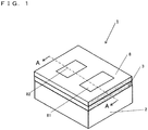
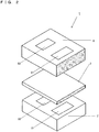
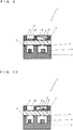
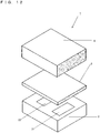
- an optical sensor device 1 includes a substrate 2, a first transparent substrate 3, a light shielding film 4, a light-emitting element 5, a light-receiving element 6, and a second transparent substrate 8.
- the substrate 2 may be rectangular in a plan view.
- the substrate 2 may be formed by laminating a plurality of dielectric layers.
- the dimensions of the substrate 2 range from 0.5 mm to 5 mm, and its thickness ranges from 0.5 mm to 5 mm in a plan view.
- the dielectric layers of the substrate 2 may be made of, for example, a ceramic material or an organic material.
- the substrate 2 is a wiring substrate made of a ceramic material (a ceramic wiring substrate)
- conductors such as connection pads, interconnections, and signal traces are formed in the dielectric layers made of the ceramic material.
- Ceramic material contained in the ceramic wiring substrate examples include sintered aluminum oxide, sintered mullite, sintered silicon carbide, sintered aluminum nitride, sintered silicon nitride, and sintered glass ceramic.
- the substrate 2 is a wiring substrate made of an organic material (an organic wiring substrate)
- a wiring conductor such as signal traces to be described later is formed in an insulating layer made of the organic material.
- the organic wiring substrate is formed from a plurality of organic dielectric layers.
- the organic wiring substrate may be any as long as it includes dielectric layers made of an organic material, such as a printed wiring substrate, a build-up wiring substrate, or a flexible wiring substrate.
- Examples of the organic material contained in the organic wiring substrate include an epoxy resin, a polyimide resin, a polyester resin, an acryl resin, a phenolic resin, and a fluorine resin.
- This substrate 2 includes at least two recesses as openings.
- One of the two recesses is a first opening 21 for accommodating the light-receiving element 6, and the other of the two recesses is a second opening 22 for accommodating the light-emitting element 5.
- the first opening 21 and the second opening 22 are formed to be opened on the same principal surface 21 of the substrate 2 (the first surface of the substrate 2).
- the optical sensor device 1 is preferably used as a measurement sensor that measures the flow of fluid such as the bloodstream, with the optical Doppler effect.
- the measurement sensor includes the light-emitting element 5 that irradiates an object to be measured with light, and the light-receiving element 6 that receives the light scattered by the object to be measured to take advantage of the optical Doppler effect.
- the measurement sensor irradiates a part of the body, for example, a finger with light from the outside. Then, the measurement sensor receives the light scattered by the blood cells contained in the blood that flows through the blood vessel under the skin, and measures the bloodstream from changes in the frequency.
- the light-emitting element 5 and the light-receiving element 6 are disposed at a predetermined distance, based on the position relationship between the irradiated light and the scattered light.
- the first opening 21 and the second opening 22 are formed according to the position relationship between the light-emitting element 5 and the light-receiving element 6.
- each of the light-emitting element 5 and the light-receiving element 6 ranges, for example, from 0.1 mm ⁇ 0.1 mm ⁇ 0.1 mm to 1.5 mm ⁇ 1.5 mm ⁇ 1.2 mm.
- the second opening 22 may be, for example, rectangular or square.
- the second opening 22 has a vertical dimension ranging from 0.3 mm to 2.0 mm, a horizontal dimension ranging from 0.3 mm to 2.0 mm, and a depth ranging from 0.3 mm to 1.0 mm.
- the first opening 21 may be, for example, rectangular or square.
- the first opening 21 has a vertical dimension ranging from 0.3 mm to 2.0 mm, a horizontal dimension ranging from 0.3 mm to 2.0 mm, and a depth ranging from 0.4 mm to 1.5 mm.
- the first opening 21 and the second opening 22 may be spaced apart to the extent that the light emitted by the light-emitting element 5 does not directly enter the light-receiving element 6. Furthermore, forming a lightproof wall between the first opening 21 and the second opening 22 (between the light-emitting element 5 and the light-receiving element 6) can shorten a distance between the first opening 21 and the second opening 22 (between the light-emitting element 5 and the light-receiving element 6). For example, the center of the first opening 21 may be placed to overlap the center of the light-receiving element 6, and the center of the second opening 22 may be placed to overlap the center of the light-emitting element 5 in planar perspective.
- the first opening 21 and the second opening 22 may be, for example, circular, square, or rectangular, or of another shape.
- Each of the first opening 21 and the second opening 22 may have a uniform cross-section parallel to the principal surface of the substrate 2 in the depth direction.
- each of the first opening 21 and the second opening 22 may be a stepped recess having a uniform cross-section identical to that of its opening up to a predetermined depth and a uniform cross-section smaller than the former one from the predetermined depth to the bottom.
- the bottom of the first opening 21 includes a region for mounting the light-receiving element 6, and the bottom of the second opening 22 includes a region for mounting the light-emitting element 5. Furthermore, a connection pad electrically connected to the light-emitting element 5 or the light-receiving element 6 is placed on the stepped surface.
- the substrate 2 may include signal traces which are electrically connected to the light-emitting element 5 or the light-receiving element 6, through which an electrical signal is transmitted to the light-emitting element 5, and through which an electrical signal is output from the light-receiving element 6.
- the signal traces may include a bonding wire that is a connection part to be connected to the light-emitting element 5 or the light-receiving element 6, a connection pad to which the bonding wire is connected, a via conductor electrically connected to the connection pad and extending from immediately below the connection pad to the lower surface of the substrate 2 (the second surface of the substrate 2), and an external connection terminal electrically connected to the via conductor.
- the external connection terminal is disposed on the lower surface of the substrate 2, and is electrically connected to a connection terminal of an external mounting substrate on which the measurement sensor including the optical sensor device 1 is mounted, with a terminal connection material such as solder.
- a nickel layer 0.5 ⁇ m to 10 ⁇ m thick and a metal layer 0.5 ⁇ m to 5 ⁇ m thick may be deposited in turn by the plating technique for increasing the wettability with a bonding material such as solder and increasing the corrosion resistance.
- the first transparent substrate 3 covers the upper surface of the substrate 2 (the first surface of the substrate 2), and is bonded to the first surface of the substrate 2 through the bonding material.
- the first transparent substrate 3 closes and seals the first opening 21 and the second opening 22 accommodating the light-receiving element 6 and the light-emitting element 5, respectively.
- the first transparent substrate 3 is a plate-shaped component made of an insulating material, and the first transparent substrate 3 may be composed of a material having optical transparency allowing the light emitted from the light-emitting element 5 accommodated in the second opening 22 to pass through the first transparent substrate 3 and allowing the light received by the light-receiving element 6 accommodated in the first opening 21 to pass through the first transparent substrate 3.
- Semiconductor laser elements such as the VCSEL can be used as the light-emitting element 5, and various photodiodes including a silicon photodiode, a GaAs photodiode, an InGaAs photodiode, and a germanium photodiode can be used as the light-receiving element 6.
- various photodiodes including a silicon photodiode, a GaAs photodiode, an InGaAs photodiode, and a germanium photodiode can be used as the light-receiving element 6.
- the VCSEL functioning as the light-emitting element 5 may be the one that can emit laser light with a wavelength of 850 nm.
- selecting the light-emitting element 5 that emits laser light with a wavelength that fits the measurement purpose will suffice.
- the light-receiving element 6 may be any as long as it can receive the light emitted from the light-emitting element 5 in the absence of change in the wavelength of the light. If the wavelength of the light is changed, the light-receiving element 6 may be the one that can receive the light with the changed wavelength.
- connection pad is electrically connected to the connection pad by, for example, a bonding wire 32 in this embodiment
- another connection method such as flip chip bonding, bump connections, or connection using an anisotropic conductive film may be used.
- the first transparent substrate 3 needs to allow the irradiated light to the object to be measured and the scattered light through. Since the characteristics of the irradiated light and the scattered light are determined by a light-emitting element to be mounted, the first transparent substrate 3 may be structured to allow at least the light emitted from the light-emitting element to be mounted through.
- the first transparent substrate 3 is composed of the insulating material whose transmittance of the light with the wavelength that is emitted from the light-emitting element is higher than or equal to 70%, preferably, higher than or equal to 90% will suffice.
- Examples of the insulating material of the first transparent substrate 3 can include a transparent ceramic material such as sapphire, a glass material, and a resin material.
- Examples of the glass material can include borosilicate glass, crystallized glass, quartz, and soda glass.
- Examples of the resin material can include a polycarbonate resin, an unsaturated polyester resin, and an epoxy resin.
- the first transparent substrate 3 is, for example, rectangular in a plan view. The dimensions of the first transparent substrate 3 range from 0.5 mm ⁇ 1 mm to 5 mm ⁇ 5 mm. Furthermore, the first transparent substrate 3 is 0.5 mm to 5 mm thick.
- the bonding material bonds the substrate 2 to the first transparent substrate 3. Specifically, the bonding material bonds an upper surface of the substrate 2 to a lower surface of the first transparent substrate 3 at the periphery.
- the bonding material is ring-shaped on the upper surface of the substrate 2, and is a sealant for maintaining the airtightness and the water-tightness in the first opening 21 and the second opening 22 of the substrate 2. Since the light-receiving element 6 and the light-emitting element 5 accommodated in the first opening 21 and the second opening 22, respectively, are susceptible to, for example, moisture, the bonding material is shaped into a ring without a seam to reduce the entry of external moisture.
- the bonding material may be lightproof. This lightproof effect of the bonding material can reduce external light entering the first opening 21 and the second opening 22 through the substrate 2 and the first transparent substrate 3.
- the lightproof effect of the bonding material may be achieved by absorption of light. Although the lightproof effect may be achieved by reflection of light from the viewpoint of reducing the entry of external light, the stray light generated inside the measurement sensor may be reflected off the bonding material and further received by the light-receiving element. If the bonding material is the one that absorbs the light, the bonding material can absorb the external light to reduce the entry of the external light, and can also absorb the stray light generated inside.
- the bonding material functioning as a material with the lightproof effect through absorption of light is obtained by, for example, dispersing a light absorbing material into a resin adhesive with capability of bonding the substrate 2 and the first transparent substrate 3, such as an epoxy resin or a conductive silicon resin.
- the light absorbing material can include inorganic pigments.
- the inorganic pigments can include a carbon-based pigment such as carbon black, a nitride-based pigment such as titanium black, and a metal oxide-based pigment such as Cr-Fe-Co system, Cu-Co-Mn system, Fe-Co-Mn system, or Fe-Co-Ni-Cr system.
- the bonding material may be made of a metal material such as solder. Examples of the metal material can include brazing filler metals such as Sn-Ag, Sn-Ag-Cu, Au-Sn, Au-Sn-Ag, and Au-Si.
- the light shielding film 4 may be placed on the lower surface of the first transparent substrate 3.
- the light shielding film 4 is formed by, for example, vapor-depositing, sputtering, or baking a metal material, for example, a metal, e.g., Cr, Ti, Al, Cu, Co, Ag, Au, Pd, Pt, Ru, Sn, Ta, Fe, In, Ni, or W, or an alloy of some of these metals.
- the light shielding film 4 is, for example, 50 nm to 400 nm thick.
- the light shielding film 4 is placed to overlap the light-emitting element 5. The overlapping herein indicates a state where the light shielding film 4 covers a part of the light-emitting element 5.
- the light shielding film 4 partially includes a through hole through which at least the light emitted by the light-emitting element 5 and the reflected light that reaches the light-receiving element 6 pass.
- the light shielding film 4 may be placed on the upper surface of the second transparent substrate 8 to be described later. This can reduce the incidence of unnecessary scattered light onto the light-receiving element 6.
- a first through hole 81 is, for example, circular or rectangular, and the dimensions range from ⁇ 50 ⁇ m to ⁇ 1 mm.
- a second through hole 82 is, for example, circular or rectangular, and the dimensions range from ⁇ 5 ⁇ m to ⁇ 500 ⁇ m.
- the second transparent substrate 8 according to the first embodiment of the present disclosure includes the first through hole 81 in a position overlapping the first opening 21.
- the second transparent substrate 8 includes the second through hole 82 in a position overlapping the second opening 22 and at a distance from the first through hole 81.
- a lens 9 is placed in the first through hole 81.
- the second transparent substrate 8 is placed on the upper surface of the first transparent substrate 3.
- the second transparent substrate 8 can be made of, for example, a transparent ceramic material such as sapphire, a glass material, or a resin material.
- the glass material can include borosilicate glass, crystallized glass, quartz, and soda glass.
- the resin material can include a polycarbonate resin, an unsaturated polyester resin, and an epoxy resin.
- the dimensions of the second transparent substrate 8 may be the same as those of the first transparent substrate 3 in a plan view.
- the thickness of the second transparent substrate 8 may be any with consideration given to a distance to a target object.
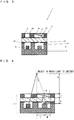
- the lens 9 has a first sloped surface S1.
- the first sloped surface S1 is sloped downward from the light-emitting element 5 side to the light-receiving element 6 side (sloped from the left side to the right side in FIG. 3 ).
- the first sloped surface S1 is more sloped toward the first transparent substrate 3 as it comes closer from the light-emitting element 5 side to the light-receiving element 6 side in a cross-sectional view.
- the lens is thicker from the inside of the substrate 2 toward the outside of the substrate 2.
- the cross-sectional view herein means a cross-section in a vertical direction and a direction of connecting the centers of the light-emitting element 5 and the light-receiving element 6 in the optical device 1.
- the optical sensor device 1 includes the lens 9 with the first sloped surface S1.
- the light reflected off the surface of a target object reference light
- more intense light reflected off the target object measured light
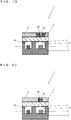
- a lower surface of the second transparent substrate 8 includes a first diffractive lens 91 whose surface is convex and concave in a position overlapping the first opening 21 in a plan view as illustrated in FIGS. 13 and 14 .
- the concave portions and the convex portions may be alternately and concentrically arranged from the center of the first diffractive lens 91, particularly, from the position overlapping the light-receiving element 6 in a plan view toward the outside.
- the convex portions of the first diffractive lens 91 may have third sloped surfaces S3 toward the center. The slope angles of the third sloped surfaces S3 may be gradually increased with respect to a direction perpendicular to the thickness direction of the second transparent substrate 8.
- the slope angles are angles of the slopes with respect to the plane such as the upper surface and the lower surface of the second transparent substrate 8.
- the convex portions, only the concave portions, or the convex portions and the concave portions may be alternately and concentrically arranged from the center toward the outside in a plan view.
- the spaces between the convex portions and the concave portions may be narrower toward the outside.
- the first diffractive lens 91 with such a concentric arrangement can be, for example, a spherical lens.
- the first diffractive lens 91 can be produced by micromachining the surface.
- the third sloped surfaces S3 of sloped convex portions can reduce the incidence of the light reflected off an object other than a target object and the reflected light that has an angle of reflection larger than that of the target object onto the light-receiving element 6.
- the third sloped surfaces S3 enable the light to be easily totally reflected.
- the concentric arrangement can reduce the incidence of the reflected light that has an angle of reflection larger than that of the target object onto the light-receiving element 6 in any direction, or enables the light to be easily totally reflected.
- the reflected light means the light emitted from the light-emitting element 5 and reflected off a target object or a certain object other than the target object.
- the upper surface of the second transparent substrate 8 may include a second diffractive lens 92 whose surface is convex and concave in a position overlapping the second opening 22 in a plan view.
- the convex portions of the second diffractive lens 92 may have fourth sloped surfaces S4 toward the center. Only the convex portions, only the concave portions, or the convex portions and the concave portions may be alternately and concentrically arranged from the center, particularly, from the position overlapping the light-emitting element 5 in a plan view toward the outside. Furthermore, the slope angles of the fourth sloped surfaces S4 may be increased with respect to the thickness direction of the second transparent substrate 8 and the vertical direction.
- only the convex portions, only the concave portions, or the convex portions and the concave portions may be alternately and concentrically arranged from the center toward the outside in a plan view.
- the spaces between the convex portions and the concave portions may be narrower toward the outside.
- the second diffractive lens 92 with such a concentric arrangement can be, for example, a spherical lens.
- the second diffractive lens 92 can be produced by micromachining the surface.
- the sloped convex portions can focus the light by the fourth sloped surfaces S4, and allow the light from the light-emitting element 5 to concentratedly hit a target object.
- the concentric arrangement allows the light incident from the light-emitting element 5 in any direction to be easily focused.
- the optical sensor device 1 includes the first diffractive lens 91 in the position overlapping the light-receiving element 6. This can totally reflect the light including the reference light except the desired light to be measured. Alternatively, this can keep the position at which the light including the reference light except the desired light to be measured is focused from overlapping the light-receiving element 6. Consequently, the magnitude of signal light incident on the light-receiving element 6 can be relatively increased.
- the second transparent substrate 8 includes a first region R1 and a second region R2 with different refractive indexes, in positions overlapping the first opening 21 in a plan view.
- a plurality of regions including the first region R1 and the second region R2 involve the plane and the thickness direction.
- the first region R1 and the second region R2 may be concentrically arranged in order from the center of the plurality of regions, particularly, from the positions overlapping the light-receiving element 6 toward the outside.
- a region with a different refractive index may be placed outside the first region R1 and the second region R2.
- regions with different refractive indexes may be concentrically arranged in positions overlapping the first opening 21 in a plan view.
- the boundary between the first region R1 and the second region R2 may be sloped so that each of the first region R1 and the second region R2 has a lower surface smaller than an upper surface, and in the second transparent substrate 8, a boundary of the second region R2 opposite to the boundary between the first region R1 and the second region R2 may have a slope angle larger than that of the boundary between the first region R1 and the second region R2.
- the second transparent substrate 8 may include the plurality of regions with different refractive indexes, and the plurality of regions may be concentrically arranged. Specifically, the plurality of regions may be concentrically arranged from the center of the plurality of regions toward the outside in a plan view with respect to the lower surface of the second transparent substrate 8. The widths of the regions may be narrower toward the outside. For example, a spherical lens may be bonded for use as the second transparent substrate 8 with the concentric arrangement. Furthermore, the second transparent substrate 8 can be produced by micromachining, for example, changing a refractive index using laser light. The concentric arrangement can reduce the incidence of the reflected light that has an angle of reflection larger than that of the target object onto the light-receiving element 6 in any direction, or enables the light to be easily totally reflected.
- the second transparent substrate 8 includes a third region R3 and a fourth region R4 with different refractive indexes, in positions overlapping the second opening 22 in a plan view.
- the third region R3 and the fourth region R4 may be concentrically arranged in order from the center of the plurality of regions, particularly, from the position overlapping the light-emitting element 5 toward the outside in a plan view.
- the boundary between the third region R3 and the fourth region R4 may be sloped so that each of the third region R3 and the fourth region R4 has a lower surface larger than an upper surface, and in the second transparent substrate 8, a boundary of the fourth region R4 opposite to the boundary between the third region R3 and the fourth region R4 may have a slope angle larger than that of the boundary between the third region R3 and the fourth region R4.
- the plurality of regions may be concentrically arranged from the center of the regions toward the outside in a plan view with respect to the upper surface of the second transparent substrate 8.
- the widths of the regions may be narrower toward the outside.
- a spherical lens may be bonded for use as the second transparent substrate 8 with the concentric arrangement.
- the second transparent substrate 8 can be produced by micromachining, for example, changing a refractive index using laser light. The concentric arrangement allows the light incident from the light-emitting element 5 in any direction to be easily focused.
- the optical sensor device 1 includes the first region R1 and the second region R2 with different refractive indexes, in the positions overlapping the light-receiving element 6. This can totally reflect the light including the reference light except the desired light to be measured. Alternatively, this can keep the position at which the light including the reference light except the desired light to be measured is focused from overlapping the light-receiving element 6. Consequently, the magnitude of the light incident on the light-receiving element 6 can be relatively increased.
- the substrate 2 is produced in a method for manufacturing a multilayer wiring substrate.
- the substrate 2 is a ceramic wiring substrate and is made of alumina as its ceramic material
- feedstock powder such as alumina (Al 2 O 3 ), silica (SiO 2 ), calcia (CaO), or magnesia (MgO) with an appropriate organic solvent or an appropriate solvent
- This slurry is molded into a sheet by a known method such as doctor-blading or calendar roll to obtain a ceramic green sheet (hereinafter may be referred to as a green sheet).
- the green sheet is die cut into a predetermined shape.
- admixing feedstock powder such as tungsten (W) or a glass material with an organic solvent or a solvent produces a metal paste.
- This metal paste is pattern printed on the surface of the green sheet in a printing method such as screen printing.
- a via conductor is produced by forming a through hole on the green sheet and filling the through hole with the metal paste by, for example, the screen printing.
- a metallized layer to be, for example, a ground conductor is formed on the top surface using the metal paste. Laminating a plurality of the green sheets obtained in such a manner, and simultaneously firing the green sheets at a temperature approximately 1600°C produce the substrate 2.
- the first transparent substrate 3 is prepared by cutting a glass material into a predetermined shape through, for example, trimming or cutting-off.
- the light shielding film 4 to be described later is formed on the lower surface of the first transparent substrate 3 through, for example, vapor-deposition, sputtering, or baking.
- the via conductors are aligned in the vertical direction in the substrate 2, the via conductors need not be aligned but may be formed in the substrate 2 with displacements, for example, through inner layer wiring or using an inner ground conductor layer as long as they are electrically connected from the upper surface of the substrate 2 to the external connection terminal on the lower surface.
- machining or an imprint technique using a die may be applied to the second transparent substrate 8, similarly to the method for manufacturing the first transparent substrate 3 and the lens 9, etc.
- the machining include a method for directly processing a rectangular parallelepiped transparent substrate, and a method for embedding a lens or a sloped glass separately produced into a pierced base substrate and fixing the lens or the sloped glass to the base substrate using, for example, an adhesive.
- the first sloped surface S1 of the lower surface of the lens 9 may have a slope angle at which the reflected light larger than the light reflected off a target object is totally reflected. This structure can reduce the incidence of light other than a target object, and increase the intensity of the light reflected off the target object. Thus, more accurate measurement can be performed.
- ⁇ 1 denotes an angle of reflection at which the light emitted from the light-emitting element 5 hits fluid, for example, the blood as a target object and is reflected off
- ⁇ 2 denotes an angle of reflection at which the light hits an object covering the fluid as the target object, for example, the surface of the blood vessel and is reflected off
- ⁇ is the one illustrated in FIG. 4 .
- the refractive index of the lens 9 may be larger than that of air. If this is applied to the equation above, n1 is the refractive index of air, and n2 is the refractive index of the lens 9. Increase in the refractive index of n2 can cause the total reflection of light with ease.
- h denotes a distance from an object for reflection to the upper surface of the lens 9 with the first sloped surface S1
- d denotes the thickness of the second transparent substrate 8
- g denotes a distance from the lens 9 with the first sloped surface S1 to the light receiver
- r denotes a half of the width of the light receiver
- L denotes a horizontal distance from the object for reflection to the center of the light receiver
- W denotes a horizontal distance from the right end of the lens 9 with the first sloped surface S1 to a light receiving point
- n denotes the refractive index of the lens 9 with the first sloped surface S1
- ⁇ , ⁇ , and ⁇ denote angles.
- W ((L - htan ⁇ - dtan ⁇ )(1 - tan ⁇ tan ⁇ ) - gtan ⁇ (1 - tan ⁇ tan ⁇ ))/(tan ⁇ (tan ⁇ -tan ⁇ )) holds.
- W1 ((L ⁇ r - htan ⁇ - dtan ⁇ )(1-tan ⁇ tan ⁇ ) - gtan ⁇ (1 - tan ⁇ tan ⁇ ))/(tan ⁇ (tan ⁇ - tan ⁇ )) holds.
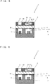
- the upper surface of the lens 9 may be sloped from the light-emitting element 5 side to the light-receiving element 6 side in a cross-sectional view.
- the upper surface of the lens 9 may include a second sloped surface S2.
- the second sloped surface S2 is sloped upward. This enables the light to be more easily totally reflected.
- the upper surface of the lens 9 closer to the light-emitting element 5 as illustrated in FIG. 5 or the entirety of the upper surface may be sloped, so that only the reference light is easily totally reflected.
- only a part of the lower surface of the lens 9 closer to the light-emitting element 5 or the entirety of the lower surface may be sloped, so that only the reference light is easily totally reflected.
- the lens 9 may be sloped symmetrically in the vertical direction.
- the upper surface and the lower surface of the lens 9 may be partly sloped.
- a first condenser lens 11 may be attached to the upper surface of the first transparent substrate 3 below the lens 9, in a position overlapping the first opening 21 and the first through hole 81 in the optical sensor device 1 according to the other embodiment of the present disclosure.
- the dimensions of the first condenser lens 11 range from ⁇ 20 ⁇ m to ⁇ 2 mm, and its thickness ranges from 0.5 mm to 2 mm in a plan view.
- the first condenser lens 11 is made of, for example, a glass material such as quartz glass or borosilicate glass, or a resin material such as acryl, polycarbonate, styrene, or polyolefine.
- the first condenser lens 11 may have optical transparency allowing the light emitted from the light-emitting element 5 to pass through the light-receiving element 6.
- the first condenser lens 11 may have the properties of refracting, in an optical axis direction, light through, for example, a convex lens with light focusing properties.
- the first condenser lens 11 can improve the light focusing properties toward the light-receiving element 6 by refracting the diffused light that is the light irradiated from the light-emitting element 5 to make converging rays or collimated light.
- a second condenser lens 12 may be further attached to the upper surface of the first transparent substrate 3 in a position overlapping the second opening 22 and the second through hole 82.
- the dimensions of the second condenser lens 12 range from ⁇ 70 ⁇ m to ⁇ 2 mm, and its thickness ranges from 50 ⁇ m to 2 mm in a plan view.
- the second condenser lens 12 is made of, for example, a glass material such as quartz glass or borosilicate glass, or a resin material such as acryl, polycarbonate, styrene, or polyolefine.
- the second condenser lens 12 may have optical transparency allowing the light irradiated from the light-emitting element 5 through.
- the second condenser lens 12 may have the properties of refracting, in an optical axis direction, light through, for example, a convex lens with light focusing properties.
- the second condenser lens 12 can improve the light focusing properties by refracting the diffused light that is the light irradiated from the light-emitting element 5 to make converging rays or collimated light.
- the optical sensor device 1 is mounted on an external mounting substrate and used.
- a control element that controls an emission of the light-emitting element 5, and an arithmetic element that calculates the blood flow velocity, etc., from an output signal of the light-receiving element 6 are mounted on the external mounting substrate.
- the optical sensor device 1 receives the current for controlling the light-emitting element from the external mounting substrate through the external connection terminal, with the fingertip of the finger being in contact with the surface of the second transparent substrate 8 as an object to be measured (target object). Then, the light-emitting element 5 receives the current through, for example, the via conductors and the connection pad, and emits the light for measurement. When the irradiated light reaches the fingertip through the first transparent substrate 3, the light is scattered at blood cells in the blood. Upon receipt of the scattered light through the first transparent substrate 3, the light-receiving element 6 outputs an electrical signal corresponding to the amount of the received light. The output signal passes through the connection pad and the via conductors, and is sent from the optical sensor device 1 to the external mounting substrate through the external connection terminal.
- the arithmetic element receives the signal output from the optical sensor device 1.
- the arithmetic element can calculate the blood flow velocity by analyzing the intensity of the scattered light received by the light-receiving element 6 for each frequency.
- the lower surface of the first transparent substrate 3 may be spaced from the substrate 2 between the first opening 21 and the second opening 22.
- the substrate 2 includes a lightproof wall between the first opening 21 and the second opening 22, and a part of the upper end of the wall is missing. Since this enables the reference light to directly reach the light-receiving element 6, more accurate measurement can be performed.
- the optical sensor device 1 may include the first diffractive lens 91 that totally reflects the reflected light with an angle of incidence larger than that of the light reflected off a target object.
- the optical sensor device 1 may include the first diffractive lens 91 that can keep the position at which the reflected light with an angle of incidence larger than that of the light reflected off at least a target object is focused from overlapping the light-receiving element 6. This structure can reduce the incidence of the light reflected off an object other than the target object onto the light-receiving element 6, and relatively increase the intensity of the light reflected off the target object. Thus, more accurate measurement can be performed.
- first diffractive lens 91 and the second diffractive lens 92 may be of the same shape.
- the shapes and the positions of the lenses may be the same on the upper surface and the lower surface as illustrated in FIG. 13 . This facilitates the processing.
- the first diffractive lens 91 and the second diffractive lens 92 may be of different shapes.
- the lenses may have the same dimensions, or may be of the same shape and geometrically similar.
- the convex portions and the concave portions of the first diffractive lens 91 may be alternately arranged from the center of the first diffractive lens 91 toward the outside.
- the outer edge of the first diffractive lens 91 may be rectangular, and convex and concave portions may be formed to be parallel in one side of the rectangular outer edge.
- the slope angles of the third sloped surfaces S3 of the convex portions may be increased as they are more distant from a position directly above the light-receiving element 6.
- intervals between the concave portions, between the convex portions, or between the concave portions and the convex portions are narrower toward the outside of the first diffractive lens 91 with respect to the center of the first diffractive lens 91 in a plan view. This can reduce the incidence of the reflected light that has an angle of reflection larger than that of the target object onto the light-receiving element 6 in any direction.
- the second diffractive lens 92 may also include convex and concave portions alternately arranged from the center toward the outside.
- the outer edge of the second diffractive lens 92 may be rectangular, and convex and concave portions may be formed to be parallel in one side of the rectangle.
- the slope angles of the third sloped surfaces S3 of the convex and concave portions may be increased as they are more distant from a position directly above the light-emitting element 5.
- the widths of the convex and concave portions are narrower from the center toward the outside in a plan view.
- the optical sensor device 1 is advantageous because the reflected light with an angle of incidence larger than that of the light reflected off a target object can be totally reflected.
- the position at which reflected light with an angle of incidence larger than that of reflected light from at least a target object is focused can be kept from overlapping the light-receiving element 6.
- the optical sensor device 1 may include the first region R1 and the second region R2 with different refractive indexes. This structure can reduce the incidence of the light other than the target object onto the light receiver, and relatively increase the intensity of the light reflected off the target object. Thus, more accurate measurement can be performed.
- first region R1 and the third region R3, and the second region R2 and the fourth region R4 may be of the same shape, and symmetrically arranged. This facilitates the processing. Furthermore, the first region R1 and the third region R3, and the second region R2 and the fourth region R4 may be of different shapes.
- first region R1 and the second region R2 may be aligned from the center toward the outside.
- the outer edge of the first region R1 and the second region R2 may be rectangular, and the first region R1 and the second region R2 may be aligned in parallel in one side of the rectangle.
- the third region R3 and the fourth region R4 may be aligned from the center toward the outside.
- the refractive index of the second region R2 may be smaller than that of the first region R1.
- the light is easily totally reflected off a boundary surface between the first region R1 and the second region R2.
- the light incident on the light-receiving element 6 can be easily reduced.
- the present disclosure is not limited by the examples of the embodiments. Various modifications of values, etc., are possible. Furthermore, the method for mounting the elements in the embodiments is not specified. The embodiments according to the present disclosure can be combined without departing from the scope. Although application of the optical sensor device in the embodiments according to the present disclosure to a pulse oximeter is described, it is applicable to other devices operated by a pair of sensor elements of a light-emitting element and a light-receiving element, for example, an integrated proximity/ambient light sensor device, a proximity sensor device, and a distance measuring sensor device.
Landscapes
- Physics & Mathematics (AREA)
- Health & Medical Sciences (AREA)
- Life Sciences & Earth Sciences (AREA)
- General Physics & Mathematics (AREA)
- Optics & Photonics (AREA)
- Engineering & Computer Science (AREA)
- Molecular Biology (AREA)
- Cardiology (AREA)
- Physiology (AREA)
- Veterinary Medicine (AREA)
- Biophysics (AREA)
- Pathology (AREA)
- Public Health (AREA)
- Biomedical Technology (AREA)
- Heart & Thoracic Surgery (AREA)
- Medical Informatics (AREA)
- Hematology (AREA)
- Surgery (AREA)
- Animal Behavior & Ethology (AREA)
- General Health & Medical Sciences (AREA)
- Electromagnetism (AREA)
- Fluid Mechanics (AREA)
- Measuring Pulse, Heart Rate, Blood Pressure Or Blood Flow (AREA)
- Investigating Or Analysing Materials By Optical Means (AREA)
- Switches Operated By Changes In Physical Conditions (AREA)
- Photo Coupler, Interrupter, Optical-To-Optical Conversion Devices (AREA)
Applications Claiming Priority (4)
| Application Number | Priority Date | Filing Date | Title |
|---|---|---|---|
| JP2018203998 | 2018-10-30 | ||
| JP2018223473 | 2018-11-29 | ||
| JP2018223552 | 2018-11-29 | ||
| PCT/JP2019/042568 WO2020090883A1 (fr) | 2018-10-30 | 2019-10-30 | Dispositif de capteur optique |
Publications (2)
| Publication Number | Publication Date |
|---|---|
| EP3876257A1 true EP3876257A1 (fr) | 2021-09-08 |
| EP3876257A4 EP3876257A4 (fr) | 2022-08-17 |
Family
ID=70462263
Family Applications (1)
| Application Number | Title | Priority Date | Filing Date |
|---|---|---|---|
| EP19880898.2A Withdrawn EP3876257A4 (fr) | 2018-10-30 | 2019-10-30 | Dispositif de capteur optique |
Country Status (5)
| Country | Link |
|---|---|
| US (1) | US20210382319A1 (fr) |
| EP (1) | EP3876257A4 (fr) |
| JP (1) | JP7134246B2 (fr) |
| CN (1) | CN112912984A (fr) |
| WO (1) | WO2020090883A1 (fr) |
Families Citing this family (5)
| Publication number | Priority date | Publication date | Assignee | Title |
|---|---|---|---|---|
| WO2021060364A1 (fr) * | 2019-09-27 | 2021-04-01 | 富士フイルム株式会社 | Dispositif de mesure de débit |
| WO2023079951A1 (fr) * | 2021-11-05 | 2023-05-11 | パナソニックホールディングス株式会社 | Capteur de proximité et appareil de câblage le comprenant |
| JP7344333B1 (ja) * | 2022-03-22 | 2023-09-13 | 維沃移動通信有限公司 | 測距装置及び電子機器 |
| JPWO2024106014A1 (fr) | 2022-11-17 | 2024-05-23 | ||
| CN116991054B (zh) * | 2023-09-28 | 2024-03-08 | 荣耀终端有限公司 | 一种光学器件及其制作方法、可穿戴设备 |
Family Cites Families (18)
| Publication number | Priority date | Publication date | Assignee | Title |
|---|---|---|---|---|
| JPH0315129A (ja) * | 1989-06-09 | 1991-01-23 | Omron Corp | 反射型光センサ |
| JP3358099B2 (ja) * | 1994-03-25 | 2002-12-16 | オムロン株式会社 | 光学式センサ装置 |
| JP2003207578A (ja) * | 2001-11-06 | 2003-07-25 | Toto Ltd | 衛生装置 |
| JP4708214B2 (ja) * | 2006-02-23 | 2011-06-22 | 浜松ホトニクス株式会社 | 光送受信デバイス |
| JP2008010832A (ja) * | 2006-06-01 | 2008-01-17 | Nippon Telegr & Teleph Corp <Ntt> | 光学センサ、センサチップ及び生体情報測定装置 |
| US20100056887A1 (en) * | 2006-11-27 | 2010-03-04 | Pioneer Corporation | Emission sensor device and bioinformation detecting method |
| JP5128232B2 (ja) * | 2007-10-16 | 2013-01-23 | アズビル株式会社 | 反射型光電センサ |
| WO2009139030A1 (fr) * | 2008-05-12 | 2009-11-19 | パイオニア株式会社 | Dispositif de capteur lumineux |
| JP2011134463A (ja) | 2009-12-22 | 2011-07-07 | Rohm Co Ltd | 検出センサ、および検出システム |
| GB2486000A (en) * | 2010-11-30 | 2012-06-06 | St Microelectronics Res & Dev | Optical proximity detectors with arrangements for reducing internal light propagation from emitter to detector |
| JP2012133455A (ja) * | 2010-12-20 | 2012-07-12 | Mitsumi Electric Co Ltd | ポインティングデバイス |
| JP5798977B2 (ja) * | 2012-05-15 | 2015-10-21 | 日本電信電話株式会社 | 生体情報検出装置 |
| JP2015080601A (ja) * | 2013-10-23 | 2015-04-27 | セイコーエプソン株式会社 | 脈波センサー及びそれを用いた生体情報測定装置 |
| US10162047B2 (en) * | 2013-12-16 | 2018-12-25 | Kyocera Corporation | Light receiving/emitting element module and sensor device using same |
| JP2016115862A (ja) * | 2014-12-17 | 2016-06-23 | セイコーエプソン株式会社 | 画像取得装置、生体情報取得装置、電子機器 |
| JP2016131733A (ja) * | 2015-01-20 | 2016-07-25 | セイコーエプソン株式会社 | 生体情報測定装置 |
| US9752925B2 (en) * | 2015-02-13 | 2017-09-05 | Taiwan Biophotonic Corporation | Optical sensor |
| WO2017110291A1 (fr) * | 2015-12-22 | 2017-06-29 | 京セラ株式会社 | Module de capteur de mesure et capteur de mesure |
-
2019
- 2019-10-30 JP JP2020553976A patent/JP7134246B2/ja active Active
- 2019-10-30 WO PCT/JP2019/042568 patent/WO2020090883A1/fr not_active Ceased
- 2019-10-30 US US17/288,087 patent/US20210382319A1/en not_active Abandoned
- 2019-10-30 EP EP19880898.2A patent/EP3876257A4/fr not_active Withdrawn
- 2019-10-30 CN CN201980070844.4A patent/CN112912984A/zh active Pending
Also Published As
| Publication number | Publication date |
|---|---|
| WO2020090883A1 (fr) | 2020-05-07 |
| US20210382319A1 (en) | 2021-12-09 |
| JPWO2020090883A1 (ja) | 2021-10-14 |
| EP3876257A4 (fr) | 2022-08-17 |
| JP7134246B2 (ja) | 2022-09-09 |
| CN112912984A (zh) | 2021-06-04 |
Similar Documents
| Publication | Publication Date | Title |
|---|---|---|
| US20210382319A1 (en) | Optical sensor device | |
| CN111919093B (zh) | 流量流速算出装置、流量流速传感器装置、流量装置以及流量流速算出方法 | |
| JP6616496B2 (ja) | 計測センサ用パッケージおよび計測センサ | |
| JP6999407B2 (ja) | 光学センサ装置 | |
| KR102136538B1 (ko) | 계측 센서용 패키지 및 계측 센서 | |
| JP7267304B2 (ja) | 光学センサ装置 | |
| JP6659377B2 (ja) | 計測センサ用パッケージおよび計測センサ | |
| JP6718339B2 (ja) | 計測センサ用パッケージおよび計測センサ | |
| JP2018100934A (ja) | センサ装置 | |
| JP2019093078A (ja) | 光学センサ装置 | |
| JP6942211B2 (ja) | 計測センサ用パッケージおよび計測センサ | |
| JP2019058451A (ja) | 光学センサ装置 | |
| JP6753731B2 (ja) | 計測センサ用パッケージおよび計測センサ | |
| JP6462904B2 (ja) | 計測センサ用パッケージおよび計測センサ | |
| WO2020158807A1 (fr) | Capteur optique et dispositif de capteur optique faisant appel audit capteur | |
| JP6666191B2 (ja) | 計測センサ用パッケージおよび計測センサ | |
| JP7054609B2 (ja) | 計測センサ用パッケージ及び計測センサ | |
| JP6753729B2 (ja) | 計測センサ用パッケージおよび計測センサ | |
| JP2019074651A (ja) | 光学装置および光学モジュール | |
| JP6666192B2 (ja) | 計測センサ用パッケージおよび計測センサ | |
| JP2021111747A (ja) | Ledパッケージ |
Legal Events
| Date | Code | Title | Description |
|---|---|---|---|
| STAA | Information on the status of an ep patent application or granted ep patent |
Free format text: STATUS: THE INTERNATIONAL PUBLICATION HAS BEEN MADE |
|
| PUAI | Public reference made under article 153(3) epc to a published international application that has entered the european phase |
Free format text: ORIGINAL CODE: 0009012 |
|
| STAA | Information on the status of an ep patent application or granted ep patent |
Free format text: STATUS: REQUEST FOR EXAMINATION WAS MADE |
|
| 17P | Request for examination filed |
Effective date: 20210422 |
|
| AK | Designated contracting states |
Kind code of ref document: A1 Designated state(s): AL AT BE BG CH CY CZ DE DK EE ES FI FR GB GR HR HU IE IS IT LI LT LU LV MC MK MT NL NO PL PT RO RS SE SI SK SM TR |
|
| DAV | Request for validation of the european patent (deleted) | ||
| DAX | Request for extension of the european patent (deleted) | ||
| A4 | Supplementary search report drawn up and despatched |
Effective date: 20220714 |
|
| RIC1 | Information provided on ipc code assigned before grant |
Ipc: G01F 1/663 20220101ALI20220708BHEP Ipc: G02B 19/00 20060101ALI20220708BHEP Ipc: A61B 5/1455 20060101ALI20220708BHEP Ipc: H01L 31/12 20060101ALI20220708BHEP Ipc: A61B 5/0285 20060101ALI20220708BHEP Ipc: A61B 5/026 20060101ALI20220708BHEP Ipc: H01H 35/00 20060101AFI20220708BHEP |
|
| P01 | Opt-out of the competence of the unified patent court (upc) registered |
Effective date: 20230508 |
|
| STAA | Information on the status of an ep patent application or granted ep patent |
Free format text: STATUS: THE APPLICATION HAS BEEN WITHDRAWN |
|
| 18W | Application withdrawn |
Effective date: 20231005 |