EP3878249B1 - Contact traversant rempli par impression dans un substrat biface et son procédé de fabrication - Google Patents
Contact traversant rempli par impression dans un substrat biface et son procédé de fabrication Download PDFInfo
- Publication number
- EP3878249B1 EP3878249B1 EP19797668.1A EP19797668A EP3878249B1 EP 3878249 B1 EP3878249 B1 EP 3878249B1 EP 19797668 A EP19797668 A EP 19797668A EP 3878249 B1 EP3878249 B1 EP 3878249B1
- Authority
- EP
- European Patent Office
- Prior art keywords
- carrier film
- hole
- printing
- micrometers
- conductive material
- Prior art date
- Legal status (The legal status is an assumption and is not a legal conclusion. Google has not performed a legal analysis and makes no representation as to the accuracy of the status listed.)
- Active
Links
Images


Classifications
-
- H—ELECTRICITY
- H05—ELECTRIC TECHNIQUES NOT OTHERWISE PROVIDED FOR
- H05K—PRINTED CIRCUITS; CASINGS OR CONSTRUCTIONAL DETAILS OF ELECTRIC APPARATUS; MANUFACTURE OF ASSEMBLAGES OF ELECTRICAL COMPONENTS
- H05K3/00—Apparatus or processes for manufacturing printed circuits
- H05K3/40—Forming printed elements for providing electric connections to or between printed circuits
- H05K3/4038—Through-connections; Vertical interconnect access [VIA] connections
- H05K3/4053—Through-connections; Vertical interconnect access [VIA] connections by thick-film techniques
- H05K3/4069—Through-connections; Vertical interconnect access [VIA] connections by thick-film techniques for via connections in organic insulating substrates
-
- B—PERFORMING OPERATIONS; TRANSPORTING
- B42—BOOKBINDING; ALBUMS; FILES; SPECIAL PRINTED MATTER
- B42D—BOOKS; BOOK COVERS; LOOSE LEAVES; PRINTED MATTER CHARACTERISED BY IDENTIFICATION OR SECURITY FEATURES; PRINTED MATTER OF SPECIAL FORMAT OR STYLE NOT OTHERWISE PROVIDED FOR; DEVICES FOR USE THEREWITH AND NOT OTHERWISE PROVIDED FOR; MOVABLE-STRIP WRITING OR READING APPARATUS
- B42D25/00—Information-bearing cards or sheet-like structures characterised by identification or security features; Manufacture thereof
- B42D25/30—Identification or security features, e.g. for preventing forgery
- B42D25/305—Associated digital information
-
- H—ELECTRICITY
- H05—ELECTRIC TECHNIQUES NOT OTHERWISE PROVIDED FOR
- H05K—PRINTED CIRCUITS; CASINGS OR CONSTRUCTIONAL DETAILS OF ELECTRIC APPARATUS; MANUFACTURE OF ASSEMBLAGES OF ELECTRICAL COMPONENTS
- H05K3/00—Apparatus or processes for manufacturing printed circuits
- H05K3/0011—Working of insulating substrates or insulating layers
- H05K3/0017—Etching of the substrate by chemical or physical means
- H05K3/0026—Etching of the substrate by chemical or physical means by laser ablation
- H05K3/0032—Etching of the substrate by chemical or physical means by laser ablation of organic insulating material
- H05K3/0035—Etching of the substrate by chemical or physical means by laser ablation of organic insulating material of blind holes, i.e. having a metal layer at the bottom
-
- H—ELECTRICITY
- H05—ELECTRIC TECHNIQUES NOT OTHERWISE PROVIDED FOR
- H05K—PRINTED CIRCUITS; CASINGS OR CONSTRUCTIONAL DETAILS OF ELECTRIC APPARATUS; MANUFACTURE OF ASSEMBLAGES OF ELECTRICAL COMPONENTS
- H05K3/00—Apparatus or processes for manufacturing printed circuits
- H05K3/22—Secondary treatment of printed circuits
- H05K3/24—Reinforcing of the conductive pattern
- H05K3/245—Reinforcing conductive patterns made by printing techniques or by other techniques for applying conductive pastes, inks or powders; Reinforcing other conductive patterns by such techniques
-
- G—PHYSICS
- G06—COMPUTING OR CALCULATING; COUNTING
- G06K—GRAPHICAL DATA READING; PRESENTATION OF DATA; RECORD CARRIERS; HANDLING RECORD CARRIERS
- G06K19/00—Record carriers for use with machines and with at least a part designed to carry digital markings
- G06K19/06—Record carriers for use with machines and with at least a part designed to carry digital markings characterised by the kind of the digital marking, e.g. shape, nature, code
- G06K19/067—Record carriers with conductive marks, printed circuits or semiconductor circuit elements, e.g. credit or identity cards also with resonating or responding marks without active components
- G06K19/07—Record carriers with conductive marks, printed circuits or semiconductor circuit elements, e.g. credit or identity cards also with resonating or responding marks without active components with integrated circuit chips
- G06K19/077—Constructional details, e.g. mounting of circuits in the carrier
- G06K19/07749—Constructional details, e.g. mounting of circuits in the carrier the record carrier being capable of non-contact communication, e.g. constructional details of the antenna of a non-contact smart card
- G06K19/07773—Antenna details
- G06K19/07777—Antenna details the antenna being of the inductive type
- G06K19/07779—Antenna details the antenna being of the inductive type the inductive antenna being a coil
- G06K19/07783—Antenna details the antenna being of the inductive type the inductive antenna being a coil the coil being planar
-
- H—ELECTRICITY
- H05—ELECTRIC TECHNIQUES NOT OTHERWISE PROVIDED FOR
- H05K—PRINTED CIRCUITS; CASINGS OR CONSTRUCTIONAL DETAILS OF ELECTRIC APPARATUS; MANUFACTURE OF ASSEMBLAGES OF ELECTRICAL COMPONENTS
- H05K1/00—Printed circuits
- H05K1/02—Details
- H05K1/0266—Marks, test patterns or identification means
- H05K1/0268—Marks, test patterns or identification means for electrical inspection or testing
-
- H—ELECTRICITY
- H05—ELECTRIC TECHNIQUES NOT OTHERWISE PROVIDED FOR
- H05K—PRINTED CIRCUITS; CASINGS OR CONSTRUCTIONAL DETAILS OF ELECTRIC APPARATUS; MANUFACTURE OF ASSEMBLAGES OF ELECTRICAL COMPONENTS
- H05K1/00—Printed circuits
- H05K1/02—Details
- H05K1/11—Printed elements for providing electric connections to or between printed circuits
- H05K1/115—Via connections; Lands around holes or via connections
-
- H—ELECTRICITY
- H05—ELECTRIC TECHNIQUES NOT OTHERWISE PROVIDED FOR
- H05K—PRINTED CIRCUITS; CASINGS OR CONSTRUCTIONAL DETAILS OF ELECTRIC APPARATUS; MANUFACTURE OF ASSEMBLAGES OF ELECTRICAL COMPONENTS
- H05K2201/00—Indexing scheme relating to printed circuits covered by H05K1/00
- H05K2201/09—Shape and layout
- H05K2201/09209—Shape and layout details of conductors
- H05K2201/095—Conductive through-holes or vias
- H05K2201/09609—Via grid, i.e. two-dimensional array of vias or holes in a single plane
-
- H—ELECTRICITY
- H05—ELECTRIC TECHNIQUES NOT OTHERWISE PROVIDED FOR
- H05K—PRINTED CIRCUITS; CASINGS OR CONSTRUCTIONAL DETAILS OF ELECTRIC APPARATUS; MANUFACTURE OF ASSEMBLAGES OF ELECTRICAL COMPONENTS
- H05K2201/00—Indexing scheme relating to printed circuits covered by H05K1/00
- H05K2201/09—Shape and layout
- H05K2201/09209—Shape and layout details of conductors
- H05K2201/09654—Shape and layout details of conductors covering at least two types of conductors provided for in H05K2201/09218 - H05K2201/095
- H05K2201/0979—Redundant conductors or connections, i.e. more than one current path between two points
-
- H—ELECTRICITY
- H05—ELECTRIC TECHNIQUES NOT OTHERWISE PROVIDED FOR
- H05K—PRINTED CIRCUITS; CASINGS OR CONSTRUCTIONAL DETAILS OF ELECTRIC APPARATUS; MANUFACTURE OF ASSEMBLAGES OF ELECTRICAL COMPONENTS
- H05K2201/00—Indexing scheme relating to printed circuits covered by H05K1/00
- H05K2201/10—Details of components or other objects attached to or integrated in a printed circuit board
- H05K2201/10007—Types of components
- H05K2201/10098—Components for radio transmission, e.g. radio frequency identification [RFID] tag, printed or non-printed antennas
-
- H—ELECTRICITY
- H05—ELECTRIC TECHNIQUES NOT OTHERWISE PROVIDED FOR
- H05K—PRINTED CIRCUITS; CASINGS OR CONSTRUCTIONAL DETAILS OF ELECTRIC APPARATUS; MANUFACTURE OF ASSEMBLAGES OF ELECTRICAL COMPONENTS
- H05K2203/00—Indexing scheme relating to apparatus or processes for manufacturing printed circuits covered by H05K3/00
- H05K2203/14—Related to the order of processing steps
- H05K2203/1461—Applying or finishing the circuit pattern after another process, e.g. after filling of vias with conductive paste, after making printed resistors
-
- H—ELECTRICITY
- H05—ELECTRIC TECHNIQUES NOT OTHERWISE PROVIDED FOR
- H05K—PRINTED CIRCUITS; CASINGS OR CONSTRUCTIONAL DETAILS OF ELECTRIC APPARATUS; MANUFACTURE OF ASSEMBLAGES OF ELECTRICAL COMPONENTS
- H05K3/00—Apparatus or processes for manufacturing printed circuits
- H05K3/0011—Working of insulating substrates or insulating layers
- H05K3/0044—Mechanical working of the substrate, e.g. drilling or punching
- H05K3/0047—Drilling of holes
-
- H—ELECTRICITY
- H05—ELECTRIC TECHNIQUES NOT OTHERWISE PROVIDED FOR
- H05K—PRINTED CIRCUITS; CASINGS OR CONSTRUCTIONAL DETAILS OF ELECTRIC APPARATUS; MANUFACTURE OF ASSEMBLAGES OF ELECTRICAL COMPONENTS
- H05K3/00—Apparatus or processes for manufacturing printed circuits
- H05K3/10—Apparatus or processes for manufacturing printed circuits in which conductive material is applied to the insulating support in such a manner as to form the desired conductive pattern
- H05K3/12—Apparatus or processes for manufacturing printed circuits in which conductive material is applied to the insulating support in such a manner as to form the desired conductive pattern using thick film techniques, e.g. printing techniques to apply the conductive material or similar techniques for applying conductive paste or ink patterns
- H05K3/1216—Apparatus or processes for manufacturing printed circuits in which conductive material is applied to the insulating support in such a manner as to form the desired conductive pattern using thick film techniques, e.g. printing techniques to apply the conductive material or similar techniques for applying conductive paste or ink patterns by screen printing or stencil printing
-
- H—ELECTRICITY
- H05—ELECTRIC TECHNIQUES NOT OTHERWISE PROVIDED FOR
- H05K—PRINTED CIRCUITS; CASINGS OR CONSTRUCTIONAL DETAILS OF ELECTRIC APPARATUS; MANUFACTURE OF ASSEMBLAGES OF ELECTRICAL COMPONENTS
- H05K3/00—Apparatus or processes for manufacturing printed circuits
- H05K3/10—Apparatus or processes for manufacturing printed circuits in which conductive material is applied to the insulating support in such a manner as to form the desired conductive pattern
- H05K3/12—Apparatus or processes for manufacturing printed circuits in which conductive material is applied to the insulating support in such a manner as to form the desired conductive pattern using thick film techniques, e.g. printing techniques to apply the conductive material or similar techniques for applying conductive paste or ink patterns
- H05K3/1241—Apparatus or processes for manufacturing printed circuits in which conductive material is applied to the insulating support in such a manner as to form the desired conductive pattern using thick film techniques, e.g. printing techniques to apply the conductive material or similar techniques for applying conductive paste or ink patterns by ink-jet printing or drawing by dispensing
- H05K3/125—Apparatus or processes for manufacturing printed circuits in which conductive material is applied to the insulating support in such a manner as to form the desired conductive pattern using thick film techniques, e.g. printing techniques to apply the conductive material or similar techniques for applying conductive paste or ink patterns by ink-jet printing or drawing by dispensing by ink-jet printing
-
- H—ELECTRICITY
- H05—ELECTRIC TECHNIQUES NOT OTHERWISE PROVIDED FOR
- H05K—PRINTED CIRCUITS; CASINGS OR CONSTRUCTIONAL DETAILS OF ELECTRIC APPARATUS; MANUFACTURE OF ASSEMBLAGES OF ELECTRICAL COMPONENTS
- H05K3/00—Apparatus or processes for manufacturing printed circuits
- H05K3/22—Secondary treatment of printed circuits
- H05K3/24—Reinforcing of the conductive pattern
-
- H—ELECTRICITY
- H05—ELECTRIC TECHNIQUES NOT OTHERWISE PROVIDED FOR
- H05K—PRINTED CIRCUITS; CASINGS OR CONSTRUCTIONAL DETAILS OF ELECTRIC APPARATUS; MANUFACTURE OF ASSEMBLAGES OF ELECTRICAL COMPONENTS
- H05K3/00—Apparatus or processes for manufacturing printed circuits
- H05K3/40—Forming printed elements for providing electric connections to or between printed circuits
- H05K3/42—Plated through-holes or plated via connections
- H05K3/425—Plated through-holes or plated via connections characterised by the sequence of steps for plating the through-holes or via connections in relation to the conductive pattern
- H05K3/426—Plated through-holes or plated via connections characterised by the sequence of steps for plating the through-holes or via connections in relation to the conductive pattern initial plating of through-holes in substrates without metal
-
- H—ELECTRICITY
- H05—ELECTRIC TECHNIQUES NOT OTHERWISE PROVIDED FOR
- H05K—PRINTED CIRCUITS; CASINGS OR CONSTRUCTIONAL DETAILS OF ELECTRIC APPARATUS; MANUFACTURE OF ASSEMBLAGES OF ELECTRICAL COMPONENTS
- H05K3/00—Apparatus or processes for manufacturing printed circuits
- H05K3/40—Forming printed elements for providing electric connections to or between printed circuits
- H05K3/42—Plated through-holes or plated via connections
- H05K3/425—Plated through-holes or plated via connections characterised by the sequence of steps for plating the through-holes or via connections in relation to the conductive pattern
- H05K3/428—Plated through-holes or plated via connections characterised by the sequence of steps for plating the through-holes or via connections in relation to the conductive pattern initial plating of through-holes in substrates having a metal pattern
Definitions
- the present invention relates to a method for producing a through-hole plating in a carrier film printed on both sides and to a carrier film printed on both sides with through-hole plating.
- RFID labels (“radio frequency identification” labels or labels for identification using electromagnetic waves) include an antenna in the form of a conductor track printed on a film, which is connected to an RFID chip and serves both as a power supply and for communication with an RFID reader.
- the conductor track is often designed in a spiral shape and is connected to two antenna taps that are spaced apart from each other and to corresponding contacts of the RFID chip.
- the two antenna taps directly to the RFID chip by placing the RFID chip directly on the spiral conductor track, thereby connecting two distantly arranged contacts of the RFID chip to the antenna taps.
- the RFID chip acts as a bridge between the two antenna taps via the additional antenna windings located between the antenna taps.
- a via is described in which a first conductive layer is contacted with a second conductive layer via a via, wherein the via can additionally be assigned a plating.
- the EP 1 096 842 A2 describes a method for producing a multilayer printed circuit board, in which a filling step is carried out by introducing an ink to produce the via.
- the US 2011 / 0 180 310 A1 describes a structure for a printed circuit board in which an electrically conductive plate is embedded between two vias.
- the WO 2013 / 139 470 A2 describes a substrate for a portable data carrier, in particular a chip card, which has a first antenna part on one side and a second antenna part on the other side, wherein the two antenna parts can be electrically connected to one another via the through-hole contact areas.
- the US 5,203,078 A describes an identity card that is equipped with an integrated circuit (IC), which also has a through-hole connection.
- IC integrated circuit
- the WO 2005 / 117 096 A1 describes a chip module that is fixed to a substrate via an electrical through-hole with an antenna. First, a through-hole is created in the substrate and filled with a first filling material, and then the antenna is applied to the substrate by means of electrochemical deposition.
- the object of the present invention to provide an improved method for producing a carrier film printed on both sides, wherein in particular the conductivity in the area of the through-hole is further improved.
- the invention is based on and includes the finding that due to the progressive miniaturization of RFID chips, bridging the antenna windings is becoming increasingly difficult, since the distance between the contacts of the RFID chips is often smaller than the minimum distance between the two antenna taps of the conductor track that can be achieved with reasonable effort.
- the method according to the invention for producing a through-hole in a carrier film printed on both sides with conductor tracks, wherein the carrier film comprises a first side and a second side, comprises several steps.
- the first side of the carrier film is printed with electrically conductive material, covering the area of the intended through-hole.
- a through-hole is then made in the carrier film.
- the second side of the carrier film is printed with electrically conductive material, preferably partially printed.
- the through-hole is filled with electrically conductive material, preferably completely covered.
- the second side of the carrier film is printed at least once more with electrically conductive material.
- the through-hole and the electrically conductive material already printed on are filled, preferably completely covered.
- filling is to be understood as meaning that a material connection is created between the electrically conductive material printed on the first side and the second side over the entire area or the entire cross-sectional area of the through hole.
- Completely filling or filling the through hole or the volume removed in this context with electrically conductive material up to the surface of the second side is advantageous, but not absolutely necessary.
- the first side of the carrier film is preferably partially printed with electrically conductive material, namely in the area of the intended through-plating.
- the area of the intended through-plating is preferably completely covered with electrically conductive material.
- the method according to the invention has the advantage that an additional pressure step is used to apply a filling pressure, which means that more conductive material is present in the through-hole.
- a filling pressure which means that more conductive material is present in the through-hole.
- increased stability is achieved against lateral constrictions in a subsequent lamination.
- the conductivity is increased and the electrical resistance is reduced.
- the additional pressure which is also an antenna pressure. This results in higher yields and a higher tolerance towards unfavorable geometries of the through-hole. Holes with a larger aspect ratio can be filled, for example when using thicker substrates if the hole diameter cannot be increased due to the sensitivity of the exposed "membrane".
- the first side of the carrier film is printed with electrically conductive material before the through hole is made in the carrier film.
- the through hole is made after the first side has been printed, whereby the electrically conductive material already applied is retained.
- the material from the first printing step thus forms an electrically conductive end to the through hole, which ensures a good electrical connection with the electrically conductive material introduced into the through hole in the second printing step.
- conductor tracks can first be applied to the first side of the carrier film in a first printing step before, after completion of the first printing step, the filling print and conductor tracks, according to the invention as antenna print, are applied to the second side of the carrier film in a second and third printing step.
- several printing steps can be carried out simultaneously or at an overlapping time. If the through-hole is made before the first printing step or if the through-hole extends through the already applied electrically conductive material when made after the first printing step, which does not fall within the scope of the claims, it is preferred if the through-hole is dimensioned in such a way that the electrically conductive material applied in the subsequent printing steps, in particular the first and second printing steps, does not shoot through the through-hole.
- the electrically conductive material printed on one side of the carrier film should essentially not pass through the through-hole and freely exit on the other side; rather, it should remain in the through-hole in order to fill it.
- This can usually be achieved by a sufficiently small cross-section of the through hole overall or at least on the other side, adapted to the flow properties of the electrically conductive material during the printing process.
- the through hole can be shaped like a truncated cone with a cross-section that decreases towards the other side.
- Printing especially the first printing of the second side, can be done using screen printing or a jet printing process.
- other technologies are also conceivable that are suitable for increasing the amount of conductive material introduced.
- the diameter of the through hole can be 50 micrometers to 5000 micrometers.
- the diameter of the through hole is 100 micrometers to 500 micrometers.
- a corresponding diameter ensures a secure Through-hole plating with a high electrical conductivity is ensured.
- the diameter of the through-hole is preferably 50 micrometers to 200 micrometers. With conventional electrically conductive materials used for printing processes, this can prevent the material from being shot through.
- the thickness of the carrier film is preferably 20 micrometers to 250 micrometers, more preferably 50 micrometers to 100 micrometers, so that the through-hole is filled as far as possible or completely by electrically conductive material applied in one printing step.
- the thickness of the carrier film and the diameter of the through-hole are usually selected in dependence on one another, with a thicker carrier film being associated with a larger diameter of the through-hole.
- the shape of the through hole is not limited to the preferred circular design.
- the cross-sectional area of the through hole that is directly linked to the diameter information is to be taken into account, i.e. preferably 0.002 square millimeters to 20.0 square millimeters, more preferably 0.008 square millimeters to 0.2 square millimeters or 0.002 square millimeters to 0.03 square millimeters.
- the through hole can be created, for example, by punching, drilling or lasering, preferably CO2 lasers.
- the through hole should preferably be created by lasering, as this makes it easy to maintain the required accuracy.
- the electrically conductive material comprises or consists of silver conductive paste.
- Silver conductive paste is well suited for printing Conductor tracks.
- the carrier film preferably comprises polycarbonate or is made of polycarbonate.
- a carrier film made of polycarbonate can be laminated with further layers of polycarbonate to form an RFID security document constructed as a layered composite, without increasing the risk of delamination due to incompatible materials in the layers of the layered composite.
- the carrier film according to the invention printed on both sides with conductor tracks, has at least one through-hole produced according to the invention.
- a through-hole produced according to the invention.
- the through-holes which are preferably arranged closely adjacent to one another, thus establish parallel connections between the two conductor tracks, resulting in an increased cumulative electrical conductivity between the two conductor tracks.
- there is redundancy of the through-holes whereby insufficient contact in one through-hole is compensated for by successful contact in another through-hole.
- two conductor tracks on the carrier film connected by at least one via include contact points for checking the via(s).
- Test probes of a measuring device can be placed on the contact points and thus the basic existence of an electrical connection via the via(s) and/or the electrical resistance or the electrical conductivity of the via(s) can be checked.
- the RFID inlay according to the invention comprises a carrier film according to the invention and an RFID chip connected to the conductor tracks.
- the value or security document according to the invention comprises such an RFID inlay according to the invention.
- the RFID inlay according to the invention and the value or security document according to the invention have the features and advantages already mentioned above in connection with the method according to the invention and the carrier film according to the invention.
- Typical examples of a value or security document according to the present invention are identity cards, passports, driving licenses, company ID cards, credit cards, encryption cards and the like.
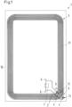
- an RFID inlay 1 as used in security documents (e.g. passports), is shown.
- the RFID inlay 1 comprises a carrier film 10 according to the invention, which is printed on both sides with conductor tracks 11.
- the conductor tracks 11 on the directly visible front side of the carrier film 10 are shown in solid lines, the conductor tracks 11 on the back side of the carrier film 10 are shown in dashed lines.
- the RFID inlay 1 also comprises the RFID chip 2, which is only indicated with a dash-dot line and is arranged on the back side of the carrier film 10.
- the RFID chip 2 of the RFID inlay 1 is connected via supply lines 3 to antenna taps 4 of an antenna 5, whereby the latter serves not only for communication purposes but also for the energy supply.
- the supply lines 3, the antenna taps 4 and the antenna 5 itself are formed by the conductor tracks 11 printed on the carrier film 10.
- the conductor track 11 is printed to form the Antenna 3 is designed in a spiral shape and is extended at the antenna taps 4 to form merely exemplary circular fields.
- the conductor tracks 11 are designed as two separate supply lines 3, each of which is connected at one end (in Figure 1 by the antenna taps 4 concealed) have, for example, circular fields analogous to the antenna taps 4 on the front.
- the two supply lines 3 are designed to converge on one another at their other ends on a common axis.
- This optional but preferred design allows the carrier film 10 to be flexibly equipped with various RFID chips 2, since the layout of the conductor tracks 11 does not prescribe a distance for the contacts of the RFID chip 2, but rather RFID chips 2 with different contact distances can be arranged on the carrier film 10 in such a way that one contact is connected to a supply line 3.
- fields of vias 12 are provided in the area of the antenna taps 4, with which the antenna taps 4 are electrically connected to the supply lines 3 and thus the antenna 5 to the RFID chip 2.
- FIGs 2a and b Two different design variants for the field of vias 12 are shown in schematic detail views, whereby the variant from Figure 2a the representation from Figure 1 The vias 12, which are actually hidden by the conductor track 11 on the front, are indicated by dotted lines.
- vias 12 are provided in the area of each antenna tap 4, each via 12 having a diameter of approximately 140 micrometers.
- each via 12 having a diameter of approximately 140 micrometers.
- five vias 12 are provided in the area of each antenna tap 4.
- the cumulative electrical conductivity of a respective field of vias 12, assuming identical materials and thickness of the carrier film 10, is practically identical.
- the invention is not limited to the number of vias 12 shown and can be implemented in individual cases with different configurations.
- the vias 12 of the carrier foil 10 of the RFID chip made of Figures 1 and 2a, b have been produced in a method according to the invention. A variant of the method according to the invention is described below with reference to the Figures 3 to 5 explained in more detail.
- the Figures 3 to 5 The carrier film 10 shown comprises a first side 21 and a second side 22. This can be a top side or bottom side or front side or back side.
- the first side 21 of the carrier film 10 is printed with electrically conductive material 13, for example silver conductive paste, in the area of the intended through-hole.
- the printing can include, for example, the printing of conductor tracks 11.
- a through hole 14 is made in the carrier film 10 from the second side 22. This can be done by means of a laser 24, preferably a CO2 laser, but also by punching or drilling.
- the second side 22 of the carrier film 10 is printed with electrically conductive material 13, for example silver conductive paste, whereby the through hole 14 is filled - preferably completely.
- electrically conductive material 13 for example silver conductive paste
- the filling pressure generated in this way is identified by the reference number 23.
- the filling pressure 23 ensures that the side surfaces and edges of the through hole 14 are completely covered with conductive material.
- the second side 22 of the carrier film 10 is printed again with electrically conductive material 13, for example silver conductive paste, whereby the through hole 14 and the filling print are covered - preferably completely.
- electrically conductive material 13 for example silver conductive paste
- the filling pressure 23 causes more conductive material to be placed in the through hole 14 or in the via 12. This results in greater mechanical stability and lower electrical resistance.
- the through hole 14 can also be made in the carrier film 10 first, for example by means of a laser 24.
- the first side 21 can then be printed with conductive material, for example as part of the printing of conductor tracks 11.
- the filling print 23 can then be applied and finally the antenna print 25.
- Multiple filling pressure steps may also be performed to further increase the amount of conductive material 13 present in the through hole 14.
- the printing of the first side 21 can also involve the antenna printing and the final printing of the second side 22, which covers the filling printing, can involve the printing of the conductor tracks. This last embodiment does not fall under the subject matter of the protection sought.
Landscapes
- Engineering & Computer Science (AREA)
- Manufacturing & Machinery (AREA)
- Microelectronics & Electronic Packaging (AREA)
- Physics & Mathematics (AREA)
- Optics & Photonics (AREA)
- Printing Elements For Providing Electric Connections Between Printed Circuits (AREA)
Claims (11)
- Procédé de génération d'un contact traversant (12) dans un film de support (10) imprimé des deux côtés avec des pistes conductrices (11) avec un premier et un second côté (21, 22), dans lequel le procédé comprend les étapes suivantes:- l'impression du premier côté (21) du film de support (10) avec un matériau électroconducteur (13), dans lequel la zone du contact traversant (12) prévu est recouverte,- après l'impression du premier côté (21), un trou traversant (14) est réalisé dans le film de support (10), dans lequel le matériau électroconducteur (13) déjà appliqué reste maintenu,- l'impression du second côté (22) du film de support (10) avec un matériau électroconducteur (13), dans lequel le trou traversant (14) s'effondre avec une pression de remplissage (23), et- au moins une autre impression du second côté (22) du film de support (10) avec un matériau électroconducteur (13), dans lequel le trou traversant (14) et le matériau électroconducteur déjà imprimé de la pression de remplissage (23) sont recouverts au moins partiellement, et dans lequel lors de l'autre impression du second côté (22) du film de support (10), une pression d'antenne (25) est appliquée en même temps à partir du matériau électroconducteur (13).
- Procédé selon la revendication 1, caractérisé en ce que l'impression est effectuée par sérigraphie ou au moyen d'un procédé d'impression par jet.
- Procédé selon l'une quelconque des revendications précédentes, caractérisé en ce que le diamètre du trou traversant (14) est compris entre 50 micromètres et 5 000 micromètres, de préférence 50 micromètres et 200 micromètres ou 100 micromètres et 500 micromètres, et/ou l'épaisseur du film de support (10) est comprise entre 20 micromètres et 250 micromètres, de préférence 75 micromètres et 125 micromètres.
- Procédé selon l'une quelconque des revendications précédentes, caractérisé en ce que le trou traversant (14) est réalisé par estampage, perçage ou émission de faisceau laser (24), de préférence laser au CO2.
- Procédé selon l'une quelconque des revendications précédentes, caractérisé en ce que le matériau électroconducteur (13) comprend une pâte d'argent conductrice.
- Procédé selon l'une quelconque des revendications précédentes, caractérisé en ce que le film de support (10) comprend du polycarbonate.
- Film de support (10) qui est imprimé des deux côtés avec des pistes conductrices (11) et présente au moins un contact traversant (12) fabriqué selon l'une quelconque des revendications précédentes.
- Film de support (10) selon la revendication 7, caractérisé en ce que respectivement une piste conductrice (11) est reliée électriquement sur différents côtés du film de support (10) par un champ d'au moins deux contacts traversants (12).
- Film de support selon la revendication 7 ou 8, caractérisé en ce que deux pistes conductrices (11) reliées par au moins un contact traversant (12) comprennent des points de contact (6) pour la vérification du contact traversant (12).
- Marqueur RFID (1) avec un film de support (10) selon l'une quelconque des revendications 7 à 9 et une puce RFID (2) reliée aux pistes conductrices (11).
- Document de valeur ou de sécurité avec un marqueur RFID selon la revendication précédente.
Applications Claiming Priority (2)
| Application Number | Priority Date | Filing Date | Title |
|---|---|---|---|
| DE102018127630.3A DE102018127630A1 (de) | 2018-11-06 | 2018-11-06 | Durchkontaktierung einer beidseitig bedruckten Trägerfolie mit Fülldruck |
| PCT/EP2019/079751 WO2020094493A1 (fr) | 2018-11-06 | 2019-10-30 | Trou d'interconnexion dans une feuille support imprimée des deux côtés |
Publications (2)
| Publication Number | Publication Date |
|---|---|
| EP3878249A1 EP3878249A1 (fr) | 2021-09-15 |
| EP3878249B1 true EP3878249B1 (fr) | 2024-12-04 |
Family
ID=68426464
Family Applications (1)
| Application Number | Title | Priority Date | Filing Date |
|---|---|---|---|
| EP19797668.1A Active EP3878249B1 (fr) | 2018-11-06 | 2019-10-30 | Contact traversant rempli par impression dans un substrat biface et son procédé de fabrication |
Country Status (3)
| Country | Link |
|---|---|
| EP (1) | EP3878249B1 (fr) |
| DE (1) | DE102018127630A1 (fr) |
| WO (1) | WO2020094493A1 (fr) |
Citations (1)
| Publication number | Priority date | Publication date | Assignee | Title |
|---|---|---|---|---|
| WO2005117096A1 (fr) * | 2004-05-31 | 2005-12-08 | Sharp Takaya Electronics Industry Co., Ltd. | Procédé de fabrication de module de circuit et module de circuit fabriqué par le procédé |
Family Cites Families (12)
| Publication number | Priority date | Publication date | Assignee | Title |
|---|---|---|---|---|
| US5203078A (en) * | 1985-07-17 | 1993-04-20 | Ibiden Co., Ltd. | Printed wiring board for IC cards |
| US5227013A (en) * | 1991-07-25 | 1993-07-13 | Microelectronics And Computer Technology Corporation | Forming via holes in a multilevel substrate in a single step |
| US5436412A (en) * | 1992-10-30 | 1995-07-25 | International Business Machines Corporation | Interconnect structure having improved metallization |
| JP3395621B2 (ja) * | 1997-02-03 | 2003-04-14 | イビデン株式会社 | プリント配線板及びその製造方法 |
| JP4300687B2 (ja) * | 1999-10-28 | 2009-07-22 | 味の素株式会社 | 接着フィルムを用いた多層プリント配線板の製造法 |
| US7211289B2 (en) * | 2003-12-18 | 2007-05-01 | Endicott Interconnect Technologies, Inc. | Method of making multilayered printed circuit board with filled conductive holes |
| DE102009050199A1 (de) * | 2009-10-21 | 2011-04-28 | Giesecke & Devrient Gmbh | Herstellung von Leiterstrukturen auf Kunststoff-Folien mittels Nanotinten |
| CN201657493U (zh) * | 2010-01-28 | 2010-11-24 | 国基电子(上海)有限公司 | 电路板 |
| DE102012005831A1 (de) * | 2012-03-22 | 2013-09-26 | Giesecke & Devrient Gmbh | Substrat für einen portablen Datenträger |
| DE102012112726A1 (de) | 2012-12-20 | 2014-06-26 | Bundesdruckerei Gmbh | Verfahren zur Herstellung eines Inlays sowie Inlay für einen Folienverbund für ein Wert- oder Sicherheitsdokument |
| US20170308781A1 (en) * | 2014-10-02 | 2017-10-26 | T-Touch International S.à.r.I. | Capacitive information carrier with improved detection accuracy by means of a via and method for the manufacture thereof |
| DE102015005690A1 (de) * | 2015-05-06 | 2016-11-10 | Pretema Gmbh | Leiterbahnstruktur mit mindestens zwei übereinanderliegenden Leiterbahnen sowie ein Verfahren zur Herstellung einer derartigen Leiterbahnstruktur |
-
2018
- 2018-11-06 DE DE102018127630.3A patent/DE102018127630A1/de not_active Withdrawn
-
2019
- 2019-10-30 WO PCT/EP2019/079751 patent/WO2020094493A1/fr not_active Ceased
- 2019-10-30 EP EP19797668.1A patent/EP3878249B1/fr active Active
Patent Citations (1)
| Publication number | Priority date | Publication date | Assignee | Title |
|---|---|---|---|---|
| WO2005117096A1 (fr) * | 2004-05-31 | 2005-12-08 | Sharp Takaya Electronics Industry Co., Ltd. | Procédé de fabrication de module de circuit et module de circuit fabriqué par le procédé |
Also Published As
| Publication number | Publication date |
|---|---|
| EP3878249A1 (fr) | 2021-09-15 |
| WO2020094493A1 (fr) | 2020-05-14 |
| DE102018127630A1 (de) | 2020-05-07 |
Similar Documents
| Publication | Publication Date | Title |
|---|---|---|
| WO1999005647A1 (fr) | Support de donnees exploitable sans contact | |
| EP1388121B1 (fr) | Procede et demi-produit destines a la fabrication d'une carte a puce comportant une bobine | |
| EP2829163B1 (fr) | Substrat pour un support de données portable | |
| EP2502471B1 (fr) | Fabrication de structures de conducteur sur des films en matière plastique au moyen de nano-encres | |
| DE19940480C2 (de) | Leiterbahnträgerschicht zur Einlaminierung in eine Chipkarte, Chipkarte mit einer Leiterbahnträgerschicht und Verfahren zur Herstellung einer Chipkarte | |
| EP3878249B1 (fr) | Contact traversant rempli par impression dans un substrat biface et son procédé de fabrication | |
| EP2817768B1 (fr) | Module électronique et support de données portatif équipé dudit module électronique et leur procédé de production | |
| EP3878246B1 (fr) | Feuille support imprimée sur ses deux faces avec trou traversant multi-niveaux et son procédé de fabrication | |
| EP3643149B1 (fr) | Trou d'interconnexion dans une feuille support imprimée des deux côtés | |
| DE202014005370U1 (de) | Induktives Bauteil | |
| DE10236666A1 (de) | Verfahren zum Herstellen von Kontaktlosen und/oder gemischten Chipkarten | |
| EP2491582B1 (fr) | Procédé de réalisation de trous métallisés | |
| DE19916781B4 (de) | Kontaktlose Chip-Karte und Herstellverfahren dazu | |
| DE102018127633B4 (de) | Verfahren zum Erzeugen einer Durchkontaktierung in einer beidseitig bedruckten Trägerfolie unter Verwendung einer diffraktiven Optik | |
| EP2210221B1 (fr) | Fabrication d'un support de données portable | |
| EP1911334B1 (fr) | Procédé et système de couplage électrique d'un support d'information avec un élement de contact | |
| WO2001016876A2 (fr) | Carte a puce et son procede de production | |
| EP2643795B1 (fr) | Configuration de circuit imprime pour un support de données portable | |
| DE102010026152A1 (de) | Kartenkörper | |
| DE102019123093A1 (de) | Verfahren zum Bearbeiten einer Schichtenstruktur und Chipkarteninlay | |
| DE102013015790A1 (de) | RFID Transponder und Verfahren zum Herstellen eines RFID Transponders |
Legal Events
| Date | Code | Title | Description |
|---|---|---|---|
| STAA | Information on the status of an ep patent application or granted ep patent |
Free format text: STATUS: UNKNOWN |
|
| STAA | Information on the status of an ep patent application or granted ep patent |
Free format text: STATUS: THE INTERNATIONAL PUBLICATION HAS BEEN MADE |
|
| PUAI | Public reference made under article 153(3) epc to a published international application that has entered the european phase |
Free format text: ORIGINAL CODE: 0009012 |
|
| STAA | Information on the status of an ep patent application or granted ep patent |
Free format text: STATUS: REQUEST FOR EXAMINATION WAS MADE |
|
| 17P | Request for examination filed |
Effective date: 20210429 |
|
| AK | Designated contracting states |
Kind code of ref document: A1 Designated state(s): AL AT BE BG CH CY CZ DE DK EE ES FI FR GB GR HR HU IE IS IT LI LT LU LV MC MK MT NL NO PL PT RO RS SE SI SK SM TR |
|
| DAV | Request for validation of the european patent (deleted) | ||
| DAX | Request for extension of the european patent (deleted) | ||
| P01 | Opt-out of the competence of the unified patent court (upc) registered |
Effective date: 20230526 |
|
| STAA | Information on the status of an ep patent application or granted ep patent |
Free format text: STATUS: EXAMINATION IS IN PROGRESS |
|
| 17Q | First examination report despatched |
Effective date: 20231020 |
|
| GRAP | Despatch of communication of intention to grant a patent |
Free format text: ORIGINAL CODE: EPIDOSNIGR1 |
|
| STAA | Information on the status of an ep patent application or granted ep patent |
Free format text: STATUS: GRANT OF PATENT IS INTENDED |
|
| INTG | Intention to grant announced |
Effective date: 20240909 |
|
| RIC1 | Information provided on ipc code assigned before grant |
Ipc: G06K 19/077 20060101ALN20240902BHEP Ipc: H05K 1/02 20060101ALN20240902BHEP Ipc: H05K 3/12 20060101ALN20240902BHEP Ipc: H05K 1/11 20060101ALN20240902BHEP Ipc: H05K 3/42 20060101ALN20240902BHEP Ipc: B42D 25/305 20140101ALI20240902BHEP Ipc: H05K 3/00 20060101ALI20240902BHEP Ipc: H05K 3/24 20060101ALI20240902BHEP Ipc: H05K 3/40 20060101AFI20240902BHEP |
|
| GRAS | Grant fee paid |
Free format text: ORIGINAL CODE: EPIDOSNIGR3 |
|
| GRAA | (expected) grant |
Free format text: ORIGINAL CODE: 0009210 |
|
| STAA | Information on the status of an ep patent application or granted ep patent |
Free format text: STATUS: THE PATENT HAS BEEN GRANTED |
|
| AK | Designated contracting states |
Kind code of ref document: B1 Designated state(s): AL AT BE BG CH CY CZ DE DK EE ES FI FR GB GR HR HU IE IS IT LI LT LU LV MC MK MT NL NO PL PT RO RS SE SI SK SM TR |
|
| REG | Reference to a national code |
Ref country code: CH Ref legal event code: EP |
|
| REG | Reference to a national code |
Ref country code: DE Ref legal event code: R096 Ref document number: 502019012617 Country of ref document: DE |
|
| REG | Reference to a national code |
Ref country code: IE Ref legal event code: FG4D Free format text: LANGUAGE OF EP DOCUMENT: GERMAN |
|
| REG | Reference to a national code |
Ref country code: LT Ref legal event code: MG9D |
|
| REG | Reference to a national code |
Ref country code: NL Ref legal event code: MP Effective date: 20241204 |
|
| PG25 | Lapsed in a contracting state [announced via postgrant information from national office to epo] |
Ref country code: HR Free format text: LAPSE BECAUSE OF FAILURE TO SUBMIT A TRANSLATION OF THE DESCRIPTION OR TO PAY THE FEE WITHIN THE PRESCRIBED TIME-LIMIT Effective date: 20241204 |
|
| PG25 | Lapsed in a contracting state [announced via postgrant information from national office to epo] |
Ref country code: FI Free format text: LAPSE BECAUSE OF FAILURE TO SUBMIT A TRANSLATION OF THE DESCRIPTION OR TO PAY THE FEE WITHIN THE PRESCRIBED TIME-LIMIT Effective date: 20241204 |
|
| PG25 | Lapsed in a contracting state [announced via postgrant information from national office to epo] |
Ref country code: BG Free format text: LAPSE BECAUSE OF FAILURE TO SUBMIT A TRANSLATION OF THE DESCRIPTION OR TO PAY THE FEE WITHIN THE PRESCRIBED TIME-LIMIT Effective date: 20241204 |
|
| PG25 | Lapsed in a contracting state [announced via postgrant information from national office to epo] |
Ref country code: ES Free format text: LAPSE BECAUSE OF FAILURE TO SUBMIT A TRANSLATION OF THE DESCRIPTION OR TO PAY THE FEE WITHIN THE PRESCRIBED TIME-LIMIT Effective date: 20241204 |
|
| PG25 | Lapsed in a contracting state [announced via postgrant information from national office to epo] |
Ref country code: NO Free format text: LAPSE BECAUSE OF FAILURE TO SUBMIT A TRANSLATION OF THE DESCRIPTION OR TO PAY THE FEE WITHIN THE PRESCRIBED TIME-LIMIT Effective date: 20250304 |
|
| PG25 | Lapsed in a contracting state [announced via postgrant information from national office to epo] |
Ref country code: LV Free format text: LAPSE BECAUSE OF FAILURE TO SUBMIT A TRANSLATION OF THE DESCRIPTION OR TO PAY THE FEE WITHIN THE PRESCRIBED TIME-LIMIT Effective date: 20241204 Ref country code: GR Free format text: LAPSE BECAUSE OF FAILURE TO SUBMIT A TRANSLATION OF THE DESCRIPTION OR TO PAY THE FEE WITHIN THE PRESCRIBED TIME-LIMIT Effective date: 20250305 |
|
| PG25 | Lapsed in a contracting state [announced via postgrant information from national office to epo] |
Ref country code: RS Free format text: LAPSE BECAUSE OF FAILURE TO SUBMIT A TRANSLATION OF THE DESCRIPTION OR TO PAY THE FEE WITHIN THE PRESCRIBED TIME-LIMIT Effective date: 20250304 |
|
| PG25 | Lapsed in a contracting state [announced via postgrant information from national office to epo] |
Ref country code: NL Free format text: LAPSE BECAUSE OF FAILURE TO SUBMIT A TRANSLATION OF THE DESCRIPTION OR TO PAY THE FEE WITHIN THE PRESCRIBED TIME-LIMIT Effective date: 20241204 |
|
| PG25 | Lapsed in a contracting state [announced via postgrant information from national office to epo] |
Ref country code: SM Free format text: LAPSE BECAUSE OF FAILURE TO SUBMIT A TRANSLATION OF THE DESCRIPTION OR TO PAY THE FEE WITHIN THE PRESCRIBED TIME-LIMIT Effective date: 20241204 |
|
| PG25 | Lapsed in a contracting state [announced via postgrant information from national office to epo] |
Ref country code: PL Free format text: LAPSE BECAUSE OF FAILURE TO SUBMIT A TRANSLATION OF THE DESCRIPTION OR TO PAY THE FEE WITHIN THE PRESCRIBED TIME-LIMIT Effective date: 20241204 |
|
| PG25 | Lapsed in a contracting state [announced via postgrant information from national office to epo] |
Ref country code: IS Free format text: LAPSE BECAUSE OF FAILURE TO SUBMIT A TRANSLATION OF THE DESCRIPTION OR TO PAY THE FEE WITHIN THE PRESCRIBED TIME-LIMIT Effective date: 20250404 |
|
| PG25 | Lapsed in a contracting state [announced via postgrant information from national office to epo] |
Ref country code: PT Free format text: LAPSE BECAUSE OF FAILURE TO SUBMIT A TRANSLATION OF THE DESCRIPTION OR TO PAY THE FEE WITHIN THE PRESCRIBED TIME-LIMIT Effective date: 20250404 |
|
| PG25 | Lapsed in a contracting state [announced via postgrant information from national office to epo] |
Ref country code: EE Free format text: LAPSE BECAUSE OF FAILURE TO SUBMIT A TRANSLATION OF THE DESCRIPTION OR TO PAY THE FEE WITHIN THE PRESCRIBED TIME-LIMIT Effective date: 20241204 |
|
| PG25 | Lapsed in a contracting state [announced via postgrant information from national office to epo] |
Ref country code: RO Free format text: LAPSE BECAUSE OF FAILURE TO SUBMIT A TRANSLATION OF THE DESCRIPTION OR TO PAY THE FEE WITHIN THE PRESCRIBED TIME-LIMIT Effective date: 20241204 |
|
| PG25 | Lapsed in a contracting state [announced via postgrant information from national office to epo] |
Ref country code: SK Free format text: LAPSE BECAUSE OF FAILURE TO SUBMIT A TRANSLATION OF THE DESCRIPTION OR TO PAY THE FEE WITHIN THE PRESCRIBED TIME-LIMIT Effective date: 20241204 |
|
| PG25 | Lapsed in a contracting state [announced via postgrant information from national office to epo] |
Ref country code: CZ Free format text: LAPSE BECAUSE OF FAILURE TO SUBMIT A TRANSLATION OF THE DESCRIPTION OR TO PAY THE FEE WITHIN THE PRESCRIBED TIME-LIMIT Effective date: 20241204 |
|
| PG25 | Lapsed in a contracting state [announced via postgrant information from national office to epo] |
Ref country code: IT Free format text: LAPSE BECAUSE OF FAILURE TO SUBMIT A TRANSLATION OF THE DESCRIPTION OR TO PAY THE FEE WITHIN THE PRESCRIBED TIME-LIMIT Effective date: 20241204 |
|
| REG | Reference to a national code |
Ref country code: DE Ref legal event code: R097 Ref document number: 502019012617 Country of ref document: DE |
|
| PG25 | Lapsed in a contracting state [announced via postgrant information from national office to epo] |
Ref country code: SE Free format text: LAPSE BECAUSE OF FAILURE TO SUBMIT A TRANSLATION OF THE DESCRIPTION OR TO PAY THE FEE WITHIN THE PRESCRIBED TIME-LIMIT Effective date: 20241204 |
|
| PG25 | Lapsed in a contracting state [announced via postgrant information from national office to epo] |
Ref country code: DK Free format text: LAPSE BECAUSE OF FAILURE TO SUBMIT A TRANSLATION OF THE DESCRIPTION OR TO PAY THE FEE WITHIN THE PRESCRIBED TIME-LIMIT Effective date: 20241204 |
|
| PLBE | No opposition filed within time limit |
Free format text: ORIGINAL CODE: 0009261 |
|
| STAA | Information on the status of an ep patent application or granted ep patent |
Free format text: STATUS: NO OPPOSITION FILED WITHIN TIME LIMIT |
|
| 26N | No opposition filed |
Effective date: 20250905 |
|
| PGFP | Annual fee paid to national office [announced via postgrant information from national office to epo] |
Ref country code: DE Payment date: 20251020 Year of fee payment: 7 |
|
| PGFP | Annual fee paid to national office [announced via postgrant information from national office to epo] |
Ref country code: GB Payment date: 20251024 Year of fee payment: 7 |
|
| PGFP | Annual fee paid to national office [announced via postgrant information from national office to epo] |
Ref country code: FR Payment date: 20251017 Year of fee payment: 7 |