EP3879655A1 - Pfc-überstromschutzschaltung und steuergerät - Google Patents
Pfc-überstromschutzschaltung und steuergerät Download PDFInfo
- Publication number
- EP3879655A1 EP3879655A1 EP19867584.5A EP19867584A EP3879655A1 EP 3879655 A1 EP3879655 A1 EP 3879655A1 EP 19867584 A EP19867584 A EP 19867584A EP 3879655 A1 EP3879655 A1 EP 3879655A1
- Authority
- EP
- European Patent Office
- Prior art keywords
- circuit
- signal
- control
- terminal
- pfc
- Prior art date
- Legal status (The legal status is an assumption and is not a legal conclusion. Google has not performed a legal analysis and makes no representation as to the accuracy of the status listed.)
- Pending
Links
- 238000005070 sampling Methods 0.000 claims abstract description 55
- 230000000630 rising effect Effects 0.000 claims description 3
- 239000003990 capacitor Substances 0.000 description 16
- 238000010586 diagram Methods 0.000 description 11
- 238000005516 engineering process Methods 0.000 description 6
- 238000000034 method Methods 0.000 description 6
- 238000012545 processing Methods 0.000 description 6
- 230000000694 effects Effects 0.000 description 2
- 230000002093 peripheral effect Effects 0.000 description 2
- 230000002035 prolonged effect Effects 0.000 description 2
- 238000004378 air conditioning Methods 0.000 description 1
- 238000012937 correction Methods 0.000 description 1
- 238000013461 design Methods 0.000 description 1
- 238000012986 modification Methods 0.000 description 1
- 230000004048 modification Effects 0.000 description 1
- 230000000750 progressive effect Effects 0.000 description 1
Images




Classifications
-
- H—ELECTRICITY
- H02—GENERATION; CONVERSION OR DISTRIBUTION OF ELECTRIC POWER
- H02H—EMERGENCY PROTECTIVE CIRCUIT ARRANGEMENTS
- H02H3/00—Emergency protective circuit arrangements for automatic disconnection directly responsive to an undesired change from normal electric working condition with or without subsequent reconnection ; integrated protection
- H02H3/08—Emergency protective circuit arrangements for automatic disconnection directly responsive to an undesired change from normal electric working condition with or without subsequent reconnection ; integrated protection responsive to excess current
- H02H3/087—Emergency protective circuit arrangements for automatic disconnection directly responsive to an undesired change from normal electric working condition with or without subsequent reconnection ; integrated protection responsive to excess current for DC applications
-
- H—ELECTRICITY
- H02—GENERATION; CONVERSION OR DISTRIBUTION OF ELECTRIC POWER
- H02P—CONTROL OR REGULATION OF ELECTRIC MOTORS, ELECTRIC GENERATORS OR DYNAMO-ELECTRIC CONVERTERS; CONTROLLING TRANSFORMERS, REACTORS OR CHOKE COILS
- H02P23/00—Arrangements or methods for the control of AC motors characterised by a control method other than vector control
- H02P23/26—Power factor control [PFC]
-
- H—ELECTRICITY
- H02—GENERATION; CONVERSION OR DISTRIBUTION OF ELECTRIC POWER
- H02H—EMERGENCY PROTECTIVE CIRCUIT ARRANGEMENTS
- H02H3/00—Emergency protective circuit arrangements for automatic disconnection directly responsive to an undesired change from normal electric working condition with or without subsequent reconnection ; integrated protection
- H02H3/02—Details
- H02H3/06—Details with automatic reconnection
- H02H3/066—Reconnection being a consequence of eliminating the fault which caused disconnection
-
- H—ELECTRICITY
- H02—GENERATION; CONVERSION OR DISTRIBUTION OF ELECTRIC POWER
- H02H—EMERGENCY PROTECTIVE CIRCUIT ARRANGEMENTS
- H02H7/00—Emergency protective circuit arrangements specially adapted for specific types of electric machines or apparatus or for sectionalised protection of cable or line systems, and effecting automatic switching in the event of an undesired change from normal working conditions
- H02H7/10—Emergency protective circuit arrangements specially adapted for specific types of electric machines or apparatus or for sectionalised protection of cable or line systems, and effecting automatic switching in the event of an undesired change from normal working conditions for converters; for rectifiers
- H02H7/12—Emergency protective circuit arrangements specially adapted for specific types of electric machines or apparatus or for sectionalised protection of cable or line systems, and effecting automatic switching in the event of an undesired change from normal working conditions for converters; for rectifiers for static converters or rectifiers
- H02H7/125—Emergency protective circuit arrangements specially adapted for specific types of electric machines or apparatus or for sectionalised protection of cable or line systems, and effecting automatic switching in the event of an undesired change from normal working conditions for converters; for rectifiers for static converters or rectifiers for rectifiers
-
- H—ELECTRICITY
- H02—GENERATION; CONVERSION OR DISTRIBUTION OF ELECTRIC POWER
- H02P—CONTROL OR REGULATION OF ELECTRIC MOTORS, ELECTRIC GENERATORS OR DYNAMO-ELECTRIC CONVERTERS; CONTROLLING TRANSFORMERS, REACTORS OR CHOKE COILS
- H02P29/00—Arrangements for regulating or controlling electric motors, appropriate for both AC and DC motors
- H02P29/02—Providing protection against overload without automatic interruption of supply
- H02P29/024—Detecting a fault condition, e.g. short circuit, locked rotor, open circuit or loss of load
- H02P29/027—Detecting a fault condition, e.g. short circuit, locked rotor, open circuit or loss of load the fault being an over-current
-
- H—ELECTRICITY
- H03—ELECTRONIC CIRCUITRY
- H03K—PULSE TECHNIQUE
- H03K17/00—Electronic switching or gating, i.e. not by contact-making and –breaking
- H03K17/08—Modifications for protecting switching circuit against overcurrent or overvoltage
- H03K17/082—Modifications for protecting switching circuit against overcurrent or overvoltage by feedback from the output to the control circuit
- H03K17/0828—Modifications for protecting switching circuit against overcurrent or overvoltage by feedback from the output to the control circuit in composite switches
-
- H—ELECTRICITY
- H03—ELECTRONIC CIRCUITRY
- H03K—PULSE TECHNIQUE
- H03K19/00—Logic circuits, i.e. having at least two inputs acting on one output; Inverting circuits
- H03K19/20—Logic circuits, i.e. having at least two inputs acting on one output; Inverting circuits characterised by logic function, e.g. AND, OR, NOR, NOT circuits
-
- H—ELECTRICITY
- H03—ELECTRONIC CIRCUITRY
- H03K—PULSE TECHNIQUE
- H03K3/00—Circuits for generating electric pulses; Monostable, bistable or multistable circuits
- H03K3/02—Generators characterised by the type of circuit or by the means used for producing pulses
- H03K3/027—Generators characterised by the type of circuit or by the means used for producing pulses by the use of logic circuits, with internal or external positive feedback
- H03K3/037—Bistable circuits
-
- H—ELECTRICITY
- H03—ELECTRONIC CIRCUITRY
- H03K—PULSE TECHNIQUE
- H03K5/00—Manipulating of pulses not covered by one of the other main groups of this subclass
- H03K5/22—Circuits having more than one input and one output for comparing pulses or pulse trains with each other according to input signal characteristics, e.g. slope, integral
- H03K5/24—Circuits having more than one input and one output for comparing pulses or pulse trains with each other according to input signal characteristics, e.g. slope, integral the characteristic being amplitude
Definitions
- the present disclosure relates to the field of circuit protection technology, and particularly, to an overcurrent protection circuit and a controller.
- Circuit overcurrent protection is a basic requirement for circuits, such as motor overcurrent protection and power factor correction (PFC) overcurrent protection.
- a motor drive circuit and a PFC circuit are widely used in an air conditioning controller, reliability of the motor drive circuit and the PFC circuit directly determines reliability of the controller.
- An overcurrent protection circuit can be used to improve the reliability of the controller.
- an overcurrent protection function is commonly realized with software, however, this has a low response speed.
- an overcurrent protection circuit and a controller are provided according to embodiments of the present disclosure, to perform circuit overcurrent protection with hardware.
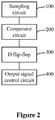
- the overcurrent protection circuit includes: a sampling circuit, a comparator circuit, a D flip-flop, and an output signal control circuit.
- the sampling circuit is configured to sample a current of a controlled circuit to obtain a sample signal, and output the sample signal to the comparator circuit.
- the comparator circuit is configured to compare the sample signal with a reference signal, generate an overcurrent signal if the sample signal is greater than the reference signal, and output the overcurrent signal to the D flip-flop.
- the D flip-flop is configured to receive the overcurrent signal, generate a first level signal in response to the overcurrent signal, and output the first level signal to the output signal control circuit.
- the output signal control circuit is configured to receive the first level signal, and output, in response to the first level signal, a control signal for reducing the current of the controlled circuit.
- overcurrent protection circuit With the above overcurrent protection circuit, a time period for overcurrent protection can be prolonged through the D flip-flop, which can increase a response speed of overcurrent protection, thereby further improving the reliability of overcurrent protection.
- a PFC overcurrent protection circuit is further provided according to an embodiment of the present disclosure, which includes: a sampling circuit, a comparator circuit, a D flip-flop, and an output signal control circuit.
- the sampling circuit is configured to sample a current of a PFC circuit to obtain a sample signal, and output the sample signal to the comparator circuit.
- the comparator circuit is configured to compare the sample signal with a reference signal, generate an overcurrent signal if the sample signal is greater than the reference signal, and output the overcurrent signal to the D flip-flop.
- the D flip-flop is configured to receive the overcurrent signal, generate a first level signal in response to the overcurrent signal, and output the first level signal to the output signal control circuit, a .
- CLR port of the D flip-flop is configured to receive a PWN control signal of a PFC main switch.
- the output signal control circuit is configured to receive the first level signal, and output, in response to the first level signal, a turn-off control signal for turning off the PFC main switch.
- the controller is configured to control an air conditioner, where the controller includes a controlled circuit and the overcurrent protection circuit according to any one of the above embodiments.
- the sampling circuit samples the output current of the PFC circuit
- the comparator circuit compares the sample signal with the reference signal, and generates the overcurrent signal if the sample signal is greater than the reference signal.
- the D flip-flop generates the first level signal in response to the overcurrent signal.
- the output signal control circuit generates, in response to the first level signal, the turn-off control signal for turning off the PFC main switch, to realize the overcurrent protection of the PFC circuit.
- the overcurrent protection circuit is operated by hardware, such that the overcurrent protection can be performed with a fast response speed and without occupying the MCU resource in the PFC circuit.
- an overcurrent protection circuit is generally arranged.
- circuits that require overcurrent protection include but are not limited to a PFC circuit, a compressor drive circuit, and a fan drive circuit.
- the compressor drive circuit and the fan drive circuit may be collectively referred to as a motor drive circuit, and a current control unit is arranged in the drive circuit.
- a current control unit of the PFC circuit and a current control unit of a motor may be used to respectively control currents in the PFC circuit and the motor drive circuit.
- FIG. 1 illustrates a schematic circuit diagram of a PFC overcurrent protection circuit.
- the PFC circuit is a boost circuit.
- the PFC circuit includes: an inductor L, a first diode D1, and an IGBT.
- a first terminal of the inductor L is connected to a positive output terminal of a rectifier bridge DB.
- the rectifier bridge DB may be considered as a pre-stage circuit of the PFC circuit, and the PFC circuit may be directly or indirectly connected to the rectifier bridge DB.
- the anode of the first diode D1 is connected to a second terminal of the inductor L, and the cathode of the first diode D1 serves as a positive output terminal of the PFC circuit and is connected to a first capacitor C1.
- a first terminal of the IGBT is connected to the second terminal of the inductor L, the IGBT function as a PFC main switch of the PFC circuit.
- the collector of the IGBT is the first terminal of the IGBT
- the base of the IGBT is a control terminal of the IGBT
- the emitter of the IGBT is a second terminal of the IGBT.
- the PFC control circuit further includes an IGBT drive circuit and a micro-processor (MCU).
- MCU micro-processor
- the main switch IGBT is turned on or turned off under control of the IGBT drive circuit, and the IGBT drive circuit is configured to control the PFC main switch IGBT to be turned on or turned off in response to a PWM control signal outputted by the micro-processor MCU.
- An output terminal of the micro-processor MCU is connected to an input terminal of the IGBT drive circuit, and is configured to provide the PWM control signal to the IGBT drive circuit, and the IGBT drive circuit is configured to control the main switch IGBT to be turned on or turned off in response to the PWM control signal. For example, if the PWM control signal is at a low level, the main switch IGBT is controlled to be turned off, and if the PWM control signal is at a high level, the main switch IGBT is controlled to be turned on.
- the PFC overcurrent protection circuit generally includes: a fist resistor R1, a ninth resistor R9, a first comparator U1, a fourth capacitor C4, a reference generation circuit, a second diode D2, a fourth resistor R4, a sixth resistor R6, an eighth resistor R8, a second resistor R2, the IGBT drive circuit, and an RC filter circuit.
- a first terminal of the first resistor R1 is connected to the second terminal of the IGBT, and a second terminal of the first resistor R1 is grounded.
- a first terminal of the ninth resistor R9 is connected to the second terminal of the IGBT.
- a non-inverting input terminal of the first comparator U1 is connected to a second terminal of the ninth resistor R9.
- the reference generation circuit is connected to an inverting input terminal of the first comparator U1.
- the reference generation circuit includes: a fifth resistor R5, a seventh resistor R7 and a second capacitor C2.
- a first terminal of the fifth resistor R5 is connected to a power supply VCC
- one terminal of the seventh resistor R7 is connected to a second terminal of the fifth resistor R5, and another terminal of the seventh resistor R7 is grounded
- the second capacitor C2 is connected in parallel with the seventh resistor R7
- the common terminal of the fifth resistor R5 and the seventh resistor R7 serves as an output terminal of the reference generation circuit.
- An output terminal of the first comparator U1 is connected to the non-inverting input terminal of the first comparator U1 through the second diode D2 and the fourth resistor R4 these are connected in series.
- One terminal of the sixth resistor R6 is connected to the output terminal of the first comparator U1, and another terminal of the sixth resistor R6 is connected to the power supply VCC.
- a first terminal of the eighth resistor R8 is connected to the output terminal of the first comparator U1, and a second terminal of the eighth resistor R8 is connected to an input terminal of the micro-processor MCU.
- a first terminal of the second resistor R2 is connected to the output terminal of the micro-processor MCU.
- An input terminal of the IGBT drive circuit is connected to a second terminal of the second resistor R2, and an output terminal of the IGBT drive circuit is connected to the control terminal of the IGBT.
- the RC filter circuit is connected to the second terminal of the second resistor R2.
- the RC filter circuit includes a third resistor R3 and a third capacitor C3 that are connected in parallel. One common terminal of the third resistor R3 and the third capacitor C3 is connected to the second terminal of the second resistor R2, and another common terminal of the third resistor R3 and the third capacitor C3 is grounded.
- an IGBT current is sampled at the second terminal of the IGBT through the first resistor R1, and a sample signal is sent to the first comparator U1.
- the first comparator detects that the sample signal exceeds a reference signal
- an output voltage of the first comparator U1 changes from a low level to a high level.
- the reference signal is a preset value that is outputted by the reference generation circuit.
- the MCU outputs a control signal in a case of detecting a change of the level, and controls the IGBT to be turned off through the IGBT drive circuit, to prevent an excessive output current of the PFC circuit, achieving an overcurrent protection effect.
- the MCU outputs the control signal by software, thus there are the following disadvantages: the response speed is slow, and many MCU resources are occupied to implement the processing process.
- the overcurrent protection circuit includes a sampling circuit 100, a comparator circuit 200, a D flip-flop 300, and an output signal control circuit 400.
- the sampling circuit 100 is configured to sample a current of a controlled circuit to obtain a sample signal, and output the sample signal to the comparator circuit 200.
- the sampling circuit 100 samples a current of a PFC circuit or a current of a motor drive circuit.
- the comparator circuit 200 is configured to compare the sample signal with a reference signal, generate an overcurrent signal if the sample signal is greater than the reference signal, and output the overcurrent signal to the D flip-flop.
- the sample signal characterizes the current of the controlled circuit.
- the reference signal corresponds to a maximum current allowed by the controlled circuit. If the current of the controlled circuit is greater than the allowed maximum current, the circuit has an overcurrent problem, and the comparator circuit generates the overcurrent signal.
- the D flip-flop 300 is configured to receive the overcurrent signal, generate a first level signal in response to the overcurrent signal, and output the first level signal to the output signal control circuit.
- the output signal control circuit 400 is configured to receive the first level signal, and output, in response to the first level signal, a control signal for reducing the current of the controlled circuit.
- the above overcurrent protection circuit is applied in a PFC circuit or a motor drive circuit.
- an operation current may be controlled by controlling an operation state of a corresponding controllable switch in response to a PWM control signal.
- a current control unit of each of the PFC circuit and the motor drive circuit generally includes a MCU chip that may output the PWM control signal.
- the overcurrent protection circuit further includes a current control unit 500.
- An input terminal of the output signal control circuit 400 is connected to the current control unit 500 and is configured to receive a PWM control signal outputted by the current control unit.
- An output terminal of the output signal control unit 400 is connected to a controllable switch for controlling the current of the controlled circuit and is configured to control the controllable switch in response to the PWM control signal and the first level signal. Specifically, if the output signal control circuit 400 does not receive the first level signal, the current control unit 500 outputs the PWM control signal through the output signal control circuit 400 to the controllable switch which is used for controlling the current of the controlled circuit, to control the current of the controlled circuit. If the output signal control circuit 400 receives the first level signal, the output signal control circuit 400 pulls down or up the PWM control signal, to prevent the output of the PWM control signal to the controllable switch which is used for controlling the current of the controlled circuit. Therefore, the controllable switch does not operate, thereby reducing the current of the controlled circuit, thus achieving the overcurrent protection effect.
- the controlled circuit may be a PFC circuit.
- the current of the controlled circuit indicates a current of the PFC circuit
- the current control circuit is a PFC control circuit.
- the sampling circuit is arranged in the PFC circuit.
- the sampling circuit is connected in series with a main switch of the PFC circuit, and the current of the PFC circuit is characterized by a current of the main switch of the PFC circuit.
- the sampling circuit is connected in series with a freewheeling diode of the PFC circuit, and the current of PFC circuit is characterized by a current of the freewheeling diode.
- the sampling circuit is directly connected in the main PFC circuit and directly samples the current of the PFC circuit.
- the sampling circuit samples the current of the PFC circuit to obtain a corresponding sampling signal.
- the comparator circuit receives the sampling signal and compares the sampling signal with the reference signal. If the sampling signal is greater than the reference signal, the comparator circuit generates an overcurrent signal and output the overcurrent signal to the D flip-flop.
- the D flip-flop generates a first level signal in response to the overcurrent signal and outputs the first level signal to the current control unit.
- the current control unit controls to reduce the current of the controlled circuit in response to the first level signal.
- the D flip-flop On the reception of the overcurrent signal, the D flip-flop can quickly generate the first level signal, and output the first level signal to the controllable switch for controlling the current of the controlled circuit, to quickly reduce the current of the controlled circuit, thereby realizing a fast response of overcurrent protection.
- the controlled circuit may also be a motor drive circuit, such as a compressor drive circuit or a fan drive circuit.
- the current of the controlled circuit indicates a drive current of the compressor or the fan.
- the current of the controlled circuit may be a drive current of each phase of the compressor or the fan, i.e. a phase current.
- the current of the controlled circuit may also be a total drive current of the compressor or the fan.
- the current control unit is a motor drive control circuit.
- an output terminal of the D flip-flop is connected to a digital IO port (i.e. a port 2) of the current control unit, and is configured to output a second level signal to the current control unit 500 in a case that the D flip-flop generates the first level signal, where the second level signal characterizes the first level signal.
- Another digital IO port (i.e. a port 3) of the current control unit 500 is connected to a reset port of the D flip-flop, and is configured to output a protection reset signal to the D flip-flop.
- the D flip-flop stops outputting the first level signal on the reception of the protection reset signal.
- the Q port may be used to generate the second level signal.
- the second level signal has an opposite level to the first level signal, that is, the first level signal is characterized by the second level signal having an opposite level to the first level signal.
- the first level signal may also be directly characterized by the first level signal, that is, if the D flip-flop 300 generates the first level signal, the D flip-flop 300 outputs the first level signal to the port 2 of the current control unit 500.
- the current control unit may determine that the circuit operates in a overcurrent protection mode.
- the current control unit 500 may be used to set a time period of overcurrent protection, that is, a time period from a time when the current control unit 500 receives the second level signal to a time when the current control unit 500 outputs the protection reset signal.
- a time period of overcurrent protection By setting the time period of overcurrent protection through the current control unit 500, the time period of overcurrent protection can be prolonged, such that reliability of the overcurrent protection can be improved and the time period of the overcurrent protection is adjustable.
- the controlled circuit includes a motor drive circuit
- a current of the motor drive circuit is obtained by an inverter circuit including six IGBTs, and the control signal for reducing the current of the controlled circuit is a control signal for turning off the IGBTs.
- the inverter circuit relates to a common technology for motor drive, which is not described herein.
- the control signal for reducing the current of the controlled circuit is a control signal for turning off the PFC main switch.
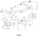
- the sampling circuit 100 includes the sampling resistor R1 connected in series with the PFC main switch, a voltage across the sampling resistor R1 is a sampling voltage, and the sampling voltage is outputted to the non-inverting input terminal of the comparator U1 in the comparator circuit 200 for comparison with the reference signal.
- the reference signal is obtained by dividing a voltage VCC by R5 and R7. If the sampling signal is very small, the sampling signal may be amplified by a signal processing circuit and then inputted to the comparator circuit 200.
- the Q port of the D flip-flop outputs a high level signal, to control a second switch Q2 to be turned on, so that a second input terminal of a second AND gate circuit U3 is inputted a low level signal.
- the second AND gate circuit U3 outputs a low level signal, and the main switch IGBT is controlled to be turned off in response to the low level signal outputted by the second AND gate circuit U3.
- the output terminal of the comparator circuit 200 is connected to a CK port of the D flip-flop, and a D port and a PR port of the D flip-flop are connected to the power supply.
- a PWM control signal output terminal (a port 1) of the MCU of the current control unit 500 is connected to the output signal control circuit 400, and is used to send the PWM control signal to the output signal control circuit 400.
- the port 2 of the MCU is connected to the Q port of the D flip-flop to receive the second level signal.
- the port 3 of the MCU is connected to the reset port (i.e. a CLR port) of the D flip-flop. In a case that the MCU receives the second level signal sent from the Q port, the MCU determines that the circuit is operated in the overcurrent protection mode.
- the port 3 After a preset time period of overcurrent protection, the port 3 sends the protection reset signal to the CLR port of the D flip-flop to exit overcurrent protection mode. After exiting the overcurrent protection mode, that is, when the circuit operates normally, the Q port outputs a low level signal, the output signal of the second AND gate circuit U3 is the PWM control signal received by the second AND gate circuit U3, so the PWM control signal is transmitted through the output signal control circuit 400 to the PFC main switch to control the current of the PFC circuit.
- the IGBT drive circuit in Figure 10 is arranged for improving the drive capability of the PWM control signal.
- Figure 10 only shows an embodiment, and the output signal control circuit 400 may also be implemented in other ways, and the D flip-flop may also be connected according to a requirement of a specific protection logic.
- the D flip-flop can be used to realize the rapid response of overcurrent protection
- the current control unit can be used to set the time period of overcurrent protection to prolong the time period of overcurrent protection, thus improving the reliability of overcurrent protection.
- an overcurrent protection circuit is further provided according to an embodiment of the present disclosure.
- the reset port of the D flip-flop is connected to the PWM control signal output terminal of the current control unit, and is configured to receive the PWM control signal, to reset the D flip-flop according to a rising edge or a falling edge of the PWM control signal, to control the D flip-flop stops outputting the first level signal.
- the reset may be performed with respect to the first level signal (that is, the D flip-flop stops outputting the first level signal), to realize the reset from the overcurrent protection mode.
- the controlled circuit includes a motor drive circuit
- the current of the motor drive circuit is obtained by an inverter circuit including six IGBTs
- the control signal for reducing the current of the controlled circuit is the control signal for turning off the IGBTs.
- the control signal for reducing the current of the controlled circuit is a control signal for turning off the main switch of the PFC circuit.
- the D flip-flop receives the overcurrent signal to generate the first level signal, and outputs the first signal to the output signal control circuit 400.
- the CLR port of the D flip-flop receives the PWM control signal outputted by the current control unit.
- the current control unit includes an MCU chip.
- the output signal control circuit receives the first level signal, the D flip-flop outputs the first level signal to the output signal control circuit, and the CLR port of the D flip-flop receives the PWM control signal outputted by the current control unit.
- the output signal control circuit receives the first level signal, and outputs, in response to the first level signal, a first control signal for reducing the current of the controlled circuit to the current control unit.
- the current control unit controls, in response to the first control signal, to reduce the current of the controlled circuit.
- the reducing the current includes reducing the current to a smaller value and turning off the current which means reducing the current to zero.
- a PFC overcurrent protection circuit is provided according to the present disclosure, which includes the sampling circuit 100, the comparator circuit 200, the D flip-flop 300, and the output signal control circuit 400.
- the sampling circuit 100 is configured to sample a current of a PFC circuit to obtain a sampling signal, and output the sampling signal to the comparator circuit.
- the sampling circuit 100 may be connected in series with a main switch IGBT in the PFC circuit, and the current flowing through the main switch IGBT is used as the current of the PFC circuit.
- the sampling circuit 100 may also be arranged in a main circuit of the PFC circuit, and the current of the PFC circuit is sampled by detecting a current in the main circuit of the PFC circuit.
- a structure of the sampling circuit 100 may be set specifically according to user requirements.
- the sampling circuit 100 may include the first resistor R1, and a first terminal of the first resistor R1 is connected to the second terminal of the main switch IGBT in the PFC circuit, the first terminal of the first resistor R1 is also connected to the first input terminal of the comparator circuit 200, and the second terminal of the first resistor R1 is grounded.
- a signal processing circuit may be arranged between the sampling circuit 100 and a non-inverting input terminal of the comparator circuit 200.
- the signal processing circuit may be a reverse processing circuit, which is configured to reverse a negative voltage for characterizing the current to obtain a positive voltage and then input the positive voltage to the non-inverting input terminal of the comparator circuit 200.
- the signal processing circuit may also be a differential circuit, which is configured to acquire a sampling voltage for characterizing the current and input the sampling voltage to the non-inverting input terminal of the comparator circuit.
- the comparator circuit 200 compares the sampling signal with the reference signal, and generates the overcurrent signal if the sampling signal is greater than the reference signal, and outputs the overcurrent signal to the D flip-flop.
- the non-inverting input terminal of the comparator circuit is connected to the output terminal of the sampling circuit.
- the comparator circuit 200 may include the first comparator U1 and a peripheral circuit thereof.
- the peripheral circuit may include: the eighth resistor R8, the sixth resistor R6, the second diode D2, the fourth resistor R4, the ninth resistor R9, and the fourth capacitor C4.
- the non-inverting input terminal of the first comparator U1 serves as the first input terminal of the comparator circuit and is connected to the output terminal of the sampling circuit 100.
- the inverting input terminal of the first comparator U1 serves as a second input terminal of the comparator circuit, and is configured to acquire the reference signal outputted by a reference generation circuit.
- the reference generation circuit is configured to provide the reference signal to the inverting input terminal of the comparator circuit 200.
- the reference generation circuit may include: the second capacitor C2, the fifth resistor R5, and the seventh resistor R7.
- the reference generation circuit may also be arranged as a part of the PFC overcurrent protection circuit.
- the D flip-flop 300 receives the overcurrent signal, generates the first level signal, and outputs the first level signal to the output signal control circuit.
- the D flip-flop 300 controls its output in response to the output signal of the comparator circuit 200. If the comparator circuit 200 outputs the overcurrent signal, the D flip-flop 300 generates and outputs the first level signal, if the comparator circuit 200 does not output the overcurrent signal, the D flip-flop 300 generates no first level signal.
- the first level signal may be a high level signal or a low level signal.
- the CLR port of the D flip-flop receives the PWM control signal for controlling the PFC main switch, for example, the PWM control signal sent by the MCU in the current control circuit 500, and takes the PWM control signal sent by the MCU as a clock signal of the D flip-flop.
- the output signal control circuit 400 receives the first level signal to generate a turn-off control signal for turning off the PFC main switch, so as to reduce the current of the PFC circuit.
- the turn-off control signal may be a low level signal.
- the output signal control circuit 400 controls the main switch IGBT in the PFC circuit to be turned off.
- the output signal control circuit 400 may directly provide a level signal to the control terminal of the main switch IGBT to control the main switch IGBT to be turned off, or the output signal control circuit 400 may provide a low level signal to the IGBT drive circuit of the main switch IGBT to control the main switch IGBT to be turned off.
- the sampling circuit 100 samples the current of the PFC circuit in real time, and the comparator circuit 200 compares the sampling voltage sampled by the sampling circuit 100 with the reference signal. If the sample signal is greater than the reference signal, the comparator circuit 200 outputs the overcurrent signal to the D flip-flop 300, and the D flip-flop generates the first level signal. In this case, the output signal control circuit 400 controls the main switch IGBT in the PFC circuit to be turned off.
- the sampling signal of the sampling circuit 100 is less than the reference signal, so the comparator circuit 200 stops outputting the overcurrent signal, and the D flip-flop 300 continues outputting the first level signal until the CLR port of the D flip-flop outputs a low level signal. Finally, the output signal control circuit 400 releases the control on the main switch IGBT, so that the PFC circuit operates normally. It can be seen that in the above process, the overcurrent protection and the release of control on the PFC circuit are implemented by hardware without using any software, so that some software resources can be released.
- a connection of ports of the D flip-flop is also described.
- the CK port of the D flip-flop is connected to the output terminal of the comparator circuit 200, the D port and PR port of the D flip-flop are pulled up and connected to the power supply.
- the D flip-flop 300 is configured to generate and output the first level signal if the CK port is inputted a high level signal.
- each port of the D flip-flop is configured as follows.
- the PR port of the D flip-flop is grounded through a fifth capacitor C5, and the D port of the D flip-flop is connected to the power supply VCC through a tenth capacitor R10, and the CLR port of the D flip-flop collects the clock signal through an eleventh capacitor R11 and is grounded through a seventh capacitor C7.
- the clock signal may be the PWM control signal provided by the MCU.
- the IGBT drive circuit controls the main switch IGBT to be turned on. In this case, there is a current flowing through the main switch IGBT, and a current of the PFC circuit flows as follows.
- the current flows from a "+" terminal of the rectifier bridge DB to the first terminal of the main switch IGBT through the inductor L, and flows out the second terminal of the main switching IGBT and then flows back to a "-" terminal of the rectifier bridge DB after passing through the first resistor R1.
- the IGBT drive circuit controls the main switch IGBT to be turned off. In this case, no current flows through the IGBT, and the current of the PFC circuit flows as follows.
- the current flows from the "+" terminal of the rectifier bridge DB to the diode D1 through the inductor L, and then flows out the diode D1 and then flows back to the "-" terminal of the rectifier bridge DB after passing through the capacitor C1.
- the current flowing from the second terminal of the main switch IGBT is sampled by using the first resistor R1, the current is converted into a corresponding voltage, and then is inputted to the non-inverting input terminal of the comparator circuit 200.
- the reference voltage provided by the reference generation circuit is inputted to the inverting input terminal of the comparator circuit 200.
- the reference generation circuit may also be arranged as a part of the overcurrent protection circuit, as illustrated in Figure 1 .
- the current passes through the main switch IGBT and is converted into the sampling voltage by the first resistor R1.
- the comparator circuit 200 compares the sampling voltage with the reference voltage. If the sampling voltage is greater than the reference voltage, it indicates that the current of the PFC circuit exceeds the set overcurrent protection value. In this case, the D flip-flop generates the first level signal.
- the D flip-flop may be connected to the output signal control circuit 400 through the Q port or the Q port, to provide the first level signal to the output signal control circuit 400 through the Q port or the Q port.
- the output terminal of the output signal control circuit 400 is connected to the control terminal of the main switch of the PFC circuit. In this case, the output terminal of the output signal control circuit 400 may be directly connected to the control terminal of the main switch.
- the output terminal of the output signal control circuit 400 may be connected to the control terminal of the main switch through the drive circuit of the main switch, as long as it can be ensured that a conduction state of the main switch changes in response to the output signal of the output signal control circuit 400.
- the output signal of the Q port or Q port of the D flip-flop may be seen in Table 1.
- Table 1 CLR PR D CK Q Q L H X X L H H H H ⁇ H L
- L represents a low level
- H represents a high level
- X represents no signal
- ⁇ represents a rising edge
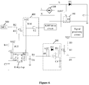
- the output signal control circuit 400 may include a third diode D3.
- the cathode of the third diode D3 serves as the input terminal of the output signal control circuit 400 and is connected to the Q port of the D flip-flop, and the anode of the third diode D3 serves as the output terminal of the output signal control circuit and is connected to the control terminal of the main switch IGBT of the PFC circuit.
- the Q port of the D flip-flop outputs a low level signal.
- signal at the anode of the third diode D3 is also at a low level, that is, the output signal control circuit 400 outputs a low level signal to the PFC circuit, and the main switching IGBT is controlled to be turned off in response to the low level signal.
- the PFC circuit outputs no current
- the comparator circuit outputs a low level signal
- the Q port of the D flip-flop continues outputting the level signal until the CLR port of the D flip-flop outputs a low level signal.
- Output of the Q port of the D flip-flop changes from a low level to a high level, and the IGBT drive circuit drives the main switch IGBT to operate normally.
- the output signal control circuit 400 may also include a first switch Q1.
- a first terminal of the first switch Q1 serves as the output terminal of the output signal control circuit, and is connected to the PFC circuit, a second terminal of the first switch Q1 is grounded.
- the control terminal of the first switch Q1 serves as the input terminal of the output signal control circuit and is connected to the Q port of the D flip-flop 300. In the solution, if the sampling signal is greater than the reference signal, the Q port of the D flip-flop outputs a high level signal.
- the first switch Q1 is turned on, and the output terminal of the first switch Q1 outputs a low level signal, that is, the output signal control circuit 400 outputs a low level signal to the PFC circuit, and the main switch IGBT is controlled to be turned off in response to the low level signal.
- the PFC circuit outputs no current
- the comparator circuit outputs a low level signal
- the Q port of the D flip-flop continues outputting a high level signal until the CLR port of the D flip-flop outputs a low level signal
- the IGBT drive circuit drives the main switch IGBT to operate normally.
- the first switch Q1 may be an NPN transistor, the base of the NPN transistor is as the input terminal, an emitter is as the output terminal, and a collector is as the control terminal.
- the output signal control circuit 400 may also include a sixteenth resistor R16 arranged between the base and the emitter of the NPN transistor, and a seventeenth resistor R17 arranged between the base of the NPN transistor and the Q port of the D flip-flop 400.
- the output signal control circuit 400 as illustrated in Figures 3 and 4 may be used as a bypass circuit and is connected to the PWM control signal input terminal of the IGBT drive circuit. That is, the output signal of the output signal control circuit 400 is superimposed with the PWM control signal outputted by the MCU to form a superimposed control signal, and the superimposed control signal is sent to the IGBT drive circuit.
- the IGBT drive circuit controls, in response to the superimposed control signal, the main switch IGBT to be turned on or off. If the output signal of the output signal control circuit 400 is at the low level, the PWM control signal is pulled down to a low level signal. In this case, the IGBT drive circuit obtains a low-level PWM control signal to control the main switch IGBT to be turned off.
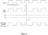
- the micro-processor MCU in the current control unit 500 continuously outputs the PWM control signal, and the current of the PFC circuit changes with the PWM control signal. If the current of the PFC circuit exceeds the set overcurrent value, the output voltage of the comparison circuit 200 changes from a low level to a high level, and the output of the Q port of the D flip-flop is controlled in response to the output signal of the comparator circuit, so that the Q port of the D flip-flop outputs a low level signal.
- the main switch IGBT is turned off in response to the low level signal, so that the current of the PFC circuit is 0 to realize overcurrent protection.
- the output current of the PFC circuit is 0, the comparator circuit 200 has no output, and the Q port of the D flip-flop continues outputting a low level signal until the CLR port of the D flip-flop outputs a low level signal. After that, the IGBT drive circuit drives the main switch IGBT to operate normally.
- the output signal control circuit 400 may also include a first AND gate circuit U2.
- a first input terminal of the first AND gate circuit U2 is configured to acquire the PWM control signal inputted to the control terminal of the main switch of the PFC circuit.
- a second input terminal of the first AND gate circuit U2 serves as the input terminal of the output signal control circuit and is connected to a power supply VCC and the Q port of the D flip-flop.
- An output terminal of the first AND gate circuit U2 serves as the output terminal of the output signal control circuit and is connected to the control terminal of the main switch of the PFC circuit, and is configured to provide to the PFC circuit the control signal that is used for controlling the main switch IGBT to be turned off.
- the Q port of the D flip-flop outputs a low level signal, to input a low level signal to the second input terminal of the first AND gate circuit U2.
- the PWM control signal inputted from the first input terminal of the first AND gate circuit U2 is at the high level. Therefore, the first AND gate circuit U2 outputs a low level signal, and the main switch IGBT is controlled to be turned off in response to the low level signal outputted by the first AND gate circuit U2.
- the output signal control circuit 400 may also include a second AND gate circuit U3 and the second switch Q2.
- a first input terminal of the second AND gate circuit U3 is configured to acquire the PWM control signal inputted to the PFC circuit
- a second input terminal of the second AND gate circuit U3 is connected to the power supply and a first terminal of the second switch Q2
- an output terminal of the second AND gate circuit U3 serves as the output terminal of the output signal control circuit and is connected to the PFC circuit.
- the first terminal of the second switch Q2 is connected to the second input terminal of the second AND gate circuit U3.
- a second terminal of the second switch Q2 is grounded.
- a control terminal of the second switch Q2 serves as the input terminal of the output signal control circuit and is connected to the Q port of the D flip-flop.
- the Q port of the D flip-flop outputs a high level signal to control the second switch Q2 to be turned on, so that the second input terminal of the second AND gate circuit U3 is inputted a low level signal.
- the PWM control signal inputted from the first input terminal of the second AND gate circuit U3 is at the high level. Therefore, the second AND gate circuit U3 outputs a low level signal, and the main switch IGBT is controlled to be turned off in response to the low level signal outputted by the second AND gate circuit U3.
- the second switch may be an NPN type transistor, a base of the NPN type transistor serves as the input terminal, the emitter serves as the output terminal, and the collector serves as the control terminal.
- the output signal control circuit 400 may also include the sixteenth resistor R16 arranged between the base and the emitter of the NPN transistor, and the seventeenth resistor R17 arranged between the base of the NPN transistor and the Q port of D flip-flop 400.
- the first AND gate circuit U2 and the second AND gate circuit U3 described in the embodiments of the present disclosure may be arranged between the micro-processor MCU of the PFC circuit and the IGBT drive circuit.
- the output signal control circuit 400 forwards the PWM control signal to the IGBT drive circuit.
- the main switch IGBT is turned off due to overcurrent, the output current of the PFC circuit is 0, and the IGBT is maintained in the off state until the CLR port of the D flip-flop outputs a low level signal.
- the input signal at the second input terminal of the first AND gate circuit U2 or the second AND gate circuit U3 becomes a high level again.
- the output signal of the first AND gate circuit U2 and the second AND gate circuit U3 has the same level as the PWM control signal. Therefore, for a next cycle of the PWM control signal, the outputs of the first AND gate circuit U2 and the second AND gate circuit U3 changes with the PWM control signal, so that the conduction state of the main switch IGBT can be controlled continuously in response to the PWM control signal.
- the overcurrent protection and the reset from the overcurrent protection mode of the PFC circuit are all performed by hardware without any software, so that some software resources can be released.
- the PFC overcurrent protection is performed pulse by pulse, so that the main switch IGBT is controlled to be turned off in a current cycle of the PWM control signal, a next PWM control signal can be normally outputted to drive the main switch IGBT in the PFC circuit, which can improve current waveform.
- a controller including the PFC overcurrent protection circuit is also provided in the present disclosure.
- the controller is configured to control an air conditioner or other load equipment.
- the controller includes the PFC circuit and the PFC overcurrent protection circuit according to any one of the above embodiments of the present disclosure.
- the PFC circuit may be the boost circuit, which includes: the inductor L, the first diode D1, and the IGBT.
- a first terminal of the inductor L is connected to the positive output terminal of the rectifier bridge DB.
- the anode of the first diode D1 is connected to a second terminal of the inductor L and the cathode of the first diode D1 is connected to a load.
- the collector of the IGBT is connected to the second terminal of the inductor L, and the emitter of the IGBT is grounded through a sampling resistor.
- the IGBT is a PFC main switch of the PFC circuit.
Landscapes
- Engineering & Computer Science (AREA)
- Power Engineering (AREA)
- Physics & Mathematics (AREA)
- Nonlinear Science (AREA)
- Computer Hardware Design (AREA)
- Computing Systems (AREA)
- General Engineering & Computer Science (AREA)
- Mathematical Physics (AREA)
- Inverter Devices (AREA)
- Protection Of Static Devices (AREA)
- Rectifiers (AREA)
- Dc-Dc Converters (AREA)
Applications Claiming Priority (2)
| Application Number | Priority Date | Filing Date | Title |
|---|---|---|---|
| CN201811144713.XA CN109301796A (zh) | 2018-09-29 | 2018-09-29 | 一种pfc过流保护电路及控制器 |
| PCT/CN2019/107772 WO2020063652A1 (zh) | 2018-09-29 | 2019-09-25 | 一种pfc过流保护电路及控制器 |
Publications (2)
| Publication Number | Publication Date |
|---|---|
| EP3879655A1 true EP3879655A1 (de) | 2021-09-15 |
| EP3879655A4 EP3879655A4 (de) | 2022-10-12 |
Family
ID=65164942
Family Applications (1)
| Application Number | Title | Priority Date | Filing Date |
|---|---|---|---|
| EP19867584.5A Pending EP3879655A4 (de) | 2018-09-29 | 2019-09-25 | Pfc-überstromschutzschaltung und steuergerät |
Country Status (4)
| Country | Link |
|---|---|
| US (1) | US11444566B2 (de) |
| EP (1) | EP3879655A4 (de) |
| CN (1) | CN109301796A (de) |
| WO (1) | WO2020063652A1 (de) |
Families Citing this family (12)
| Publication number | Priority date | Publication date | Assignee | Title |
|---|---|---|---|---|
| CN109301796A (zh) * | 2018-09-29 | 2019-02-01 | 杭州先途电子有限公司 | 一种pfc过流保护电路及控制器 |
| CN109921386A (zh) * | 2019-04-24 | 2019-06-21 | 浙江鲲悟科技有限公司 | Pfc变换器的过流保护电路及方法 |
| CN112104348B (zh) * | 2020-08-31 | 2024-11-29 | 深圳市优必选科技股份有限公司 | Mos管的保护电路 |
| CN112290506B (zh) * | 2020-09-29 | 2022-06-07 | 四川虹美智能科技有限公司 | 浪涌保护设备及方法 |
| CN112511143B (zh) * | 2020-12-15 | 2023-11-21 | 四川虹美智能科技有限公司 | Igbt保护电路和保护方法 |
| CN113285587A (zh) * | 2021-05-06 | 2021-08-20 | 珠海格力电器股份有限公司 | 一种pfc电路的保护装置及其控制方法、电机系统 |
| CN114629083A (zh) * | 2022-04-08 | 2022-06-14 | 漳州科华电气技术有限公司 | 一种过流保护电路及llc电路系统 |
| CN115201554B (zh) * | 2022-09-16 | 2023-01-13 | 中车工业研究院(青岛)有限公司 | 一种空载过流检测电路以及空载过流检测系统 |
| CN116826659B (zh) * | 2023-08-30 | 2023-12-01 | 成都爱旗科技有限公司 | 一种可调限流保护电路 |
| CN117318683B (zh) * | 2023-10-18 | 2024-06-18 | 圣邦微电子(北京)股份有限公司 | 功率晶体管的驱动电路、负载开关电路以及电源模块 |
| CN118472876A (zh) * | 2024-04-12 | 2024-08-09 | 成都火炬电子有限公司 | 一种直流高压母线的平衡电路及过流保护电路 |
| CN119420344B (zh) * | 2025-01-06 | 2025-05-23 | 浙江国利信安科技有限公司 | 信号处理电路 |
Family Cites Families (15)
| Publication number | Priority date | Publication date | Assignee | Title |
|---|---|---|---|---|
| AU2002350428A1 (en) * | 2001-11-23 | 2003-06-10 | Danfoss Drives A/S | Frequency converter for different mains voltages |
| CN101902122B (zh) * | 2010-07-29 | 2014-07-16 | 中兴通讯股份有限公司 | 一种vienna整流器逐波限流保护的方法和装置 |
| CN104170255B (zh) * | 2012-06-22 | 2017-09-19 | 富士电机株式会社 | 过电流检测装置及使用其的智能功率模块 |
| CN103078505A (zh) * | 2013-01-12 | 2013-05-01 | 华南理工大学 | 一种基于dsp的移相全桥电源模块并联电路 |
| CN104218785B (zh) * | 2013-05-31 | 2017-08-25 | 杭州先途电子有限公司 | 一种有源功率因数校正系统 |
| CN104218530B (zh) * | 2013-05-31 | 2018-06-19 | 杭州先途电子有限公司 | 一种有源pfc的硬件保护电路 |
| EP3054574B1 (de) * | 2013-09-30 | 2020-03-11 | Mitsubishi Electric Corporation | Leistungsumwandlungsvorrichtung und klimaanlage damit |
| CN203774767U (zh) * | 2014-04-22 | 2014-08-13 | 西安科技大学 | 单位功率因数boost变换器的截止型故障保护电路 |
| US20170214313A1 (en) * | 2014-05-29 | 2017-07-27 | Calsonic Kansei Corporation | Drive circuit for semiconductor switching element |
| DE112016003049T5 (de) * | 2016-02-17 | 2018-03-29 | Fuji Electric Co., Ltd. | Überstromschutzvorrichtung für halbleitervorrichtung |
| CN106486963B (zh) * | 2016-11-25 | 2018-08-31 | 西安微电子技术研究所 | 一种星用抗辐照自恢复式过流/短路保护电路 |
| CN107508473B (zh) * | 2017-07-13 | 2019-08-23 | 苏州博创集成电路设计有限公司 | 同步整流转换器 |
| CN207691769U (zh) * | 2018-01-25 | 2018-08-03 | 成都市深思创芯科技有限公司 | 一种数字可编程的相位位移电路 |
| CN109301796A (zh) | 2018-09-29 | 2019-02-01 | 杭州先途电子有限公司 | 一种pfc过流保护电路及控制器 |
| CN209344754U (zh) * | 2018-09-29 | 2019-09-03 | 杭州先途电子有限公司 | 一种pfc过流保护电路及控制器 |
-
2018
- 2018-09-29 CN CN201811144713.XA patent/CN109301796A/zh active Pending
-
2019
- 2019-09-25 WO PCT/CN2019/107772 patent/WO2020063652A1/zh not_active Ceased
- 2019-09-25 EP EP19867584.5A patent/EP3879655A4/de active Pending
- 2019-09-25 US US17/050,425 patent/US11444566B2/en active Active
Also Published As
| Publication number | Publication date |
|---|---|
| US11444566B2 (en) | 2022-09-13 |
| WO2020063652A1 (zh) | 2020-04-02 |
| US20210194405A1 (en) | 2021-06-24 |
| EP3879655A4 (de) | 2022-10-12 |
| CN109301796A (zh) | 2019-02-01 |
Similar Documents
| Publication | Publication Date | Title |
|---|---|---|
| EP3879655A1 (de) | Pfc-überstromschutzschaltung und steuergerät | |
| CN102340246B (zh) | 厚膜磁隔离直流固态功率控制器 | |
| CN101102075B (zh) | 开关元件驱动电路 | |
| JP2669117B2 (ja) | 電圧駆動形半導体素子の駆動回路 | |
| JP7042324B2 (ja) | インテリジェントパワーモジュール及びエアコン | |
| CN204967246U (zh) | Igbt短路检测保护电路及基于igbt的可控整流电路 | |
| JP2016092907A (ja) | 半導体装置 | |
| JP3780898B2 (ja) | パワーデバイスの駆動回路 | |
| CN213846230U (zh) | 一种过流保护电路 | |
| CN207884513U (zh) | 智能功率模块及空调器 | |
| CN115149782B (zh) | 高压集成电路和半导体电路 | |
| CN108063435B (zh) | 智能功率模块、空调器控制器及空调器 | |
| JP2760590B2 (ja) | 電圧駆動形素子の駆動回路 | |
| CN217486414U (zh) | 一种驱动直流电机的控制电路及按摩椅 | |
| US20240310100A1 (en) | Control Circuit Including a Controller and an Enable Module, Signal Conversion Circuit Coupled to the Controller, and Control Method | |
| CN209344754U (zh) | 一种pfc过流保护电路及控制器 | |
| WO2017206385A1 (zh) | 智能功率模块和空调器 | |
| CN110460227A (zh) | 两级式并网逆变器的驱动控制系统和驱动控制方法 | |
| CN211957318U (zh) | 一种一体化全数字无触点电磁铁控制装置 | |
| CN115622472A (zh) | 直通放电控制电路、车辆驱动模块和汽车 | |
| CN116316436A (zh) | 电机驱动电路与电子设备 | |
| CN209329673U (zh) | 过流保护电路、开关管驱动电路以及电动设备 | |
| CN201004170Y (zh) | 便携式逆变手工焊机中具有单片机控制电路 | |
| CN223625752U (zh) | 一种栅极驱动负压生成电路 | |
| CN223899203U (zh) | 一种pmos管栅极驱动电路 |
Legal Events
| Date | Code | Title | Description |
|---|---|---|---|
| STAA | Information on the status of an ep patent application or granted ep patent |
Free format text: STATUS: THE INTERNATIONAL PUBLICATION HAS BEEN MADE |
|
| PUAI | Public reference made under article 153(3) epc to a published international application that has entered the european phase |
Free format text: ORIGINAL CODE: 0009012 |
|
| STAA | Information on the status of an ep patent application or granted ep patent |
Free format text: STATUS: REQUEST FOR EXAMINATION WAS MADE |
|
| 17P | Request for examination filed |
Effective date: 20210805 |
|
| AK | Designated contracting states |
Kind code of ref document: A1 Designated state(s): AL AT BE BG CH CY CZ DE DK EE ES FI FR GB GR HR HU IE IS IT LI LT LU LV MC MK MT NL NO PL PT RO RS SE SI SK SM TR |
|
| DAV | Request for validation of the european patent (deleted) | ||
| DAX | Request for extension of the european patent (deleted) | ||
| A4 | Supplementary search report drawn up and despatched |
Effective date: 20220908 |
|
| RIC1 | Information provided on ipc code assigned before grant |
Ipc: H02H 7/125 20060101ALI20220902BHEP Ipc: H02P 29/024 20160101ALI20220902BHEP Ipc: H02P 23/26 20160101ALI20220902BHEP Ipc: H02H 3/06 20060101ALI20220902BHEP Ipc: H03K 17/082 20060101AFI20220902BHEP |