EP3879704A1 - Appareil de commande d'un dispositif de commutation et son procédé d'utilisation - Google Patents
Appareil de commande d'un dispositif de commutation et son procédé d'utilisation Download PDFInfo
- Publication number
- EP3879704A1 EP3879704A1 EP20163002.7A EP20163002A EP3879704A1 EP 3879704 A1 EP3879704 A1 EP 3879704A1 EP 20163002 A EP20163002 A EP 20163002A EP 3879704 A1 EP3879704 A1 EP 3879704A1
- Authority
- EP
- European Patent Office
- Prior art keywords
- energy store
- switching device
- switch
- control terminal
- driver circuit
- Prior art date
- Legal status (The legal status is an assumption and is not a legal conclusion. Google has not performed a legal analysis and makes no representation as to the accuracy of the status listed.)
- Granted
Links
Images

Classifications
-
- H—ELECTRICITY
- H03—ELECTRONIC CIRCUITRY
- H03K—PULSE TECHNIQUE
- H03K17/00—Electronic switching or gating, i.e. not by contact-making and –breaking
- H03K17/06—Modifications for ensuring a fully conducting state
- H03K17/063—Modifications for ensuring a fully conducting state in field-effect transistor switches
-
- H—ELECTRICITY
- H03—ELECTRONIC CIRCUITRY
- H03K—PULSE TECHNIQUE
- H03K17/00—Electronic switching or gating, i.e. not by contact-making and –breaking
- H03K17/51—Electronic switching or gating, i.e. not by contact-making and –breaking characterised by the components used
- H03K17/56—Electronic switching or gating, i.e. not by contact-making and –breaking characterised by the components used by the use, as active elements, of semiconductor devices
- H03K17/687—Electronic switching or gating, i.e. not by contact-making and –breaking characterised by the components used by the use, as active elements, of semiconductor devices the devices being field-effect transistors
-
- H—ELECTRICITY
- H03—ELECTRONIC CIRCUITRY
- H03K—PULSE TECHNIQUE
- H03K17/00—Electronic switching or gating, i.e. not by contact-making and –breaking
- H03K17/16—Modifications for eliminating interference voltages or currents
-
- H—ELECTRICITY
- H02—GENERATION; CONVERSION OR DISTRIBUTION OF ELECTRIC POWER
- H02J—ELECTRIC POWER NETWORKS; CIRCUIT ARRANGEMENTS OR SYSTEMS FOR SUPPLYING OR DISTRIBUTING ELECTRIC POWER; SYSTEMS FOR STORING ELECTRIC ENERGY
- H02J7/00—Circuit arrangements for charging or discharging batteries or for supplying loads from batteries
- H02J7/70—Circuit arrangements for charging or discharging batteries or for supplying loads from batteries characterised by the mechanical construction
- H02J7/751—Circuit arrangements for charging or discharging batteries or for supplying loads from batteries characterised by the mechanical construction concerning the insertion or the connection of the batteries
-
- H—ELECTRICITY
- H02—GENERATION; CONVERSION OR DISTRIBUTION OF ELECTRIC POWER
- H02M—APPARATUS FOR CONVERSION BETWEEN AC AND AC, BETWEEN AC AND DC, OR BETWEEN DC AND DC, AND FOR USE WITH MAINS OR SIMILAR POWER SUPPLY SYSTEMS; CONVERSION OF DC OR AC INPUT POWER INTO SURGE OUTPUT POWER; CONTROL OR REGULATION THEREOF
- H02M1/00—Details of apparatus for conversion
- H02M1/08—Circuits specially adapted for the generation of control voltages for semiconductor devices incorporated in static converters
-
- H—ELECTRICITY
- H02—GENERATION; CONVERSION OR DISTRIBUTION OF ELECTRIC POWER
- H02M—APPARATUS FOR CONVERSION BETWEEN AC AND AC, BETWEEN AC AND DC, OR BETWEEN DC AND DC, AND FOR USE WITH MAINS OR SIMILAR POWER SUPPLY SYSTEMS; CONVERSION OF DC OR AC INPUT POWER INTO SURGE OUTPUT POWER; CONTROL OR REGULATION THEREOF
- H02M1/00—Details of apparatus for conversion
- H02M1/36—Means for starting or stopping converters
-
- H—ELECTRICITY
- H03—ELECTRONIC CIRCUITRY
- H03K—PULSE TECHNIQUE
- H03K17/00—Electronic switching or gating, i.e. not by contact-making and –breaking
- H03K17/04—Modifications for accelerating switching
- H03K17/041—Modifications for accelerating switching without feedback from the output circuit to the control circuit
- H03K17/0412—Modifications for accelerating switching without feedback from the output circuit to the control circuit by measures taken in the control circuit
- H03K17/04123—Modifications for accelerating switching without feedback from the output circuit to the control circuit by measures taken in the control circuit in field-effect transistor switches
-
- H—ELECTRICITY
- H02—GENERATION; CONVERSION OR DISTRIBUTION OF ELECTRIC POWER
- H02J—ELECTRIC POWER NETWORKS; CIRCUIT ARRANGEMENTS OR SYSTEMS FOR SUPPLYING OR DISTRIBUTING ELECTRIC POWER; SYSTEMS FOR STORING ELECTRIC ENERGY
- H02J7/00—Circuit arrangements for charging or discharging batteries or for supplying loads from batteries
- H02J7/34—Parallel operation in networks using both storage and other DC sources, e.g. providing buffering
- H02J7/345—Parallel operation in networks using both storage and other DC sources, e.g. providing buffering using capacitors as storage or buffering devices
-
- H—ELECTRICITY
- H03—ELECTRONIC CIRCUITRY
- H03K—PULSE TECHNIQUE
- H03K2217/00—Indexing scheme related to electronic switching or gating, i.e. not by contact-making or -breaking covered by H03K17/00
- H03K2217/0063—High side switches, i.e. the higher potential [DC] or life wire [AC] being directly connected to the switch and not via the load
-
- H—ELECTRICITY
- H03—ELECTRONIC CIRCUITRY
- H03K—PULSE TECHNIQUE
- H03K2217/00—Indexing scheme related to electronic switching or gating, i.e. not by contact-making or -breaking covered by H03K17/00
- H03K2217/0081—Power supply means, e.g. to the switch driver
Definitions
- the present disclosure relates to an apparatus and method for driving a switching device and, in particular, a drive circuit for a MOSFET (metal-oxide-semiconductor field-effect transistor), and most particularly a power amplifier circuit.
- MOSFET metal-oxide-semiconductor field-effect transistor
- Switching devices such as High-Side N MOSFETs
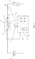
- FIG 1 shows an example of such a High-Side N MOSFET switching circuit.
- current is supplied from the vehicle's battery 1, with the positive terminal connected to the MOSFET's drain 3 and the negative terminal connected to the MOSFET's source 5 though a load 7.
- the load may be, for example, the vehicle's Engine Control Unit (ECU).
- the MOSFET's gate 6 is driven by the output 8 from a gate driver 9.
- the gate driver 9 is connected to the source 5 of the MOSFET 4 through driver terminal 10.
- An internal charge pump charges the driver capacitor 2 at a voltage higher than the battery 1 voltage.
- the gate driver's output 8 applies a driving voltage to the gate 6 which exceeds a threshold voltage, the MOSFET 4 is activated for supplying the load 7 during it's operating mode.
- Figure 1 schematically shows the concept of the gate capacitor 25 at the gate-source junction formed by the gate electrode 6 within the MOSFET 4.
- the high current MOSFET 4 has a large parasitic input capacitance C_gs. Therefore, the 'gate capacitor 25' C_gs must be charged by C_in_drv through the gate driver's output 8 before the MOSFET 4 is activated.
- the capacitance C_in_drv of driver capacitor 2 consequently needs to be greater than C_gs to cause this activation. As a result, the driver capacitor 2 takes time to charge.
- the present disclosure is therefore directed to addressing these issues.
- an apparatus comprising: a driver circuit for applying control signals to a control terminal of a switching device when activated, the switching device being activatable for driving a load in an operating mode when a control signal above a threshold voltage is applied to the control terminal; and a start-up circuit coupled to the control terminal and comprising an energy store and a switch operable to discharge the energy store for delivering a start up voltage above the threshold voltage to the control terminal for activating the switching device during a delay period before the driver circuit generates a control signal above the threshold voltage after being activated.
- the energy store may discharge rapidly, in the order of tenths of a nanosecond, to quickly activate the switching device. This thereby fills the lag time taken for the control signals generated by driver circuit to build to above the threshold voltage, after which point the driver circuit will control the switching device. In power amplifier arrangements, this provides for the rapid delivery of a high current for powering a load or loads in their operating modes.
- a low power circuit may further be provided.
- the arrangement may provide for a rapid response to a change in current demand from the load when it is woken up, and may therefore provide an uninterrupted transition from a low current supply to a high current supply.
- the apparatus further comprises a controller for actuating the switch to discharge the energy store in response an increased current demand by the load.
- the apparatus may respond automatically to a detected rise in current demand. As such, as a load is woken from its respective sleep mode and draws more current, the apparatus may respond to supply that demand.
- the energy store comprises a capacitor.
- a stored charge may be rapidly discharged to quickly apply a control signal above the threshold voltage.
- the capacitor will charge up to a predetermined level based on its capacitance and then not consume further current. As such, the capacitor can remain charged, ready for discharge upon activation of the operating mode, without compromising efficiency.
- the capacitor may be a ceramic capacitor.
- the energy store comprises charging connections for connecting the energy store to a power source for charging the energy store.
- a power source such as a battery.
- the switch comprises a bypass connection for bypassing the charging connections when the switch is operated. In this way, the charge applied to the energy store can be discharged by bypassing the energy store's connection to the power source and hence removing the potential difference applied thereby.
- the charging connections comprise a first diode for directing current discharged from the energy store to the control terminal.
- the apparatus further comprises a start-up connection for connecting the energy store to the control terminal of a switching device, wherein the start-up connection comprises a second diode for preventing current flowing from a driver circuit to the energy store.
- the second diode may thereby prevent reverse current flows from the driver circuit from charging the energy store.
- the start-up connection further comprises a resistor connected between the anode of the second diode and a negative terminal of a power source. This may thereby maintain operation of the second diode.
- the driver circuit comprises an output connection for connecting the driver circuit to the control terminal, wherein the output connection comprises a blocking component for preventing reverse current flowing to the driver circuit.
- the blocking component comprises at least one of a diode and a bypass switch.
- a diode may permit current to only flow from the driver circuit to the control terminal.
- a bypass switch may be provided in addition to the diode.
- the controller actuates the switch for recharging the energy store after a predetermined time interval following actuation to discharge the energy store.
- the time taken to activate the switching device can be predicted based on the estimated discharge characteristics of the energy store. Accordingly, following the triggering of the start-up sequence to activate the switching device, the start-up circuit can be reset to recharge the energy store for when it is needed again.
- the controller actuates the switch for recharging the energy store in response to the detection of the switching device being activated. In this way, the controller can reset the start-up circuit for recharging the energy store as soon as it is determined that the switching device has been reactivated.
- the switching device is a MOSFET. In embodiments, the switching device may be a High-Side N MOSFET. In embodiments the switching device and gate driver may provide a power amplifier circuit.
- the power supply is a battery.
- the start-up circuit, the driver circuit, and the switching device may be powered by a direct current.
- a method of activating a switching device for driving a load in an operating mode the switching device being activatable in response to a control signal above a threshold voltage being applied to a control terminal
- the method comprising: providing a driver circuit for applying control signals to the control terminal of the switching device when activated; providing a start-up circuit coupled to the control terminal and comprising an energy store for storing a charge above the threshold voltage and a switch for discharging the energy store; and operating the switch to discharge the energy store to deliver a start-up voltage to the control terminal for activating the switching device during a delay period before the driver circuit generates a control signal above the threshold voltage after being activated.
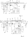
- FIG. 2 shows a first embodiment of an apparatus for providing the fast start up of a switching device 4.
- the switching device 4 is provided as High-Side N MOSFET, with a drain terminal 3, a source terminal 5, and a gate terminal 6.
- the gate terminal 6 functions as a control terminal, controlled by the output connection 8 from the driver circuit 9.
- the driver circuit 9 itself may be implemented according to various different driver circuit designs known in the art, such as a charge pump, an inductive booster, or other such power amplifier arrangement.
- Figure 5 shows an illustrative example of a gate driver circuit. As discussed above, such drive circuits 9 are known to have a delay after activation before they are able to build a sufficient voltage at the gate 6 for activating the MOSFET 4.
- the embodiment shown in Figure 2 is further provided with a starter circuit 20 which is used to deliver a start-up voltage to the MOSFET gate 6.
- the start up circuit 20 comprises an energy store or tank, provided as capacitor 11, the anode of which is connected to the positive terminal of the battery 1 through a first diode 13.
- the cathode of the capacitor 11 is connected to the negative terminal of the battery 1 through a first resistor 16, which acts to limit the current flow through the capacitor 11.
- the capacitor 11 is charged by the battery 1 up to voltage V_bat at the supply input side of the system and, once charged, the capacitor 11 will then remain charged, without consuming further current or very minimal further current.
- the capacitor 11 may be a ceramic capacitor which offers very low current leakage.
- the voltage V-bat is higher than the threshold voltage of the gate 6.
- the anode of the capacitor 11 is further connected to the MOSFET's gate 6 through starter connection 14, which includes a second diode 15.
- the second diode 15 is configured to allow current to flow to the gate 6 when the starter circuit 20 is activated, and to block reverse current from the gate driver 6 during periods when the gate driver 6 is activated.
- the starter circuit 20 is further provided with a first switch 12 connected as a bypass around the capacitor 11 and is actuatable for discharging the capacitor 11.
- a controller 24 is provided to control this first switch 11.
- the controller 24 may, for example, comprise a current load detection sensor for sensing when the current draw from the load 7 increases, along with an actuator for actuating the first switch 12 and a logic circuit for controlling the actuator based on the sensed current demand.
- the gate driver 9 In use, when the load 7 is in sleep mode, the gate driver 9 will be inactive, and hence the gate 6 will get discharged and the MOSFET 4 won't be conductive. As such, in this circuit, the load 7 is not powered by the illustrated circuit. However, it will be understood that in other embodiments, an alternative power circuit may be provided for providing a lower current to the load 7 for maintaining sleep mode operations. At the same time, the first switch 12 is open and therefore the capacitor 11 is charged by battery 1 up to voltage V_bat and held at this charged state.
- the controller 24 When a rising current demand from the load 7 is detected by the controller 24, the controller 24 actuates the first switch 12 to close. This connects the cathode of the capacitor 11 to the battery output voltage, and therefore leads to the anode of the capacitor 11 having a voltage in the range of double the battery voltage V_bat.
- the starter capacitor 11 thereby discharges starting from V_bat.
- the first diode 13 acts to block the discharged current, and thereby forces the current flow through starter connection 14 and diode 15 onto the gate 6.
- the voltage at the gate 6 therefore rises rapidly as the starter capacitor 11 discharges V_bat, causing the gate voltage to exceed the threshold. In embodiments, this discharge may be within some tenths of a nanosecond. Consequently, the MOSFET 4 is activated extremely rapidly.
- the rising current demand simultaneously prompts the activation of the gate driver 9, which begins pump charge to its driver capacitor 2.
- the voltage generated by the gate driver 9 steadily builds until the gate's threshold voltage is achieved, at which point the gate driver is able to control the gate 6.
- the output voltage from the gate driver 9 is sufficiently high to control the MOSFET 4 to continue to drive the load 7. That is, the charge from the capacitor 11 is used to activate the MOSFET 4 during the lag period when the gate driver 9 is still building its output voltage.
- the controller 24 may open the first switch 12 to reset the starter circuit and recharge the capacitor 11, ready for the next start-up operation. In embodiments, this is effected under the control of a timer set to a predetermined estimated discharge time for the capacitor 11 based on its known characteristics. In other embodiments, the controller 24 may detect that the MOSFET 4 has activated before opening the first switch 12.
- Figure 3 shows a second embodiment which operates in substantially the same way as the first embodiment but comprises additional circuit components.
- the starter circuit 20 additionally comprises a second switch 17 and a second resistor 18 connected either side of the second diode 15 along the starter connection 14.
- the second switch 17 enhances the circuit's capacity to switch off the MOSFET 4 by disconnecting the connection path between the gate 6 and the positive battery terminal through the starter connection 14.
- the starter circuit 20 further comprises a third resistor 19 and a third diode 21 along the output connection 8.
- a third switch 22 actuatable for bypassing the third diode 21 is also provided.
- the third diode 21 and third switch 22 are used to protect the gate driver 9 from reverse currents.
- the first switch 12 when the load is in sleep mode or turned off, the first switch 12 is open and therefore the capacitor 11 is charged by battery 1 up to voltage V_bat. At the same time the second switch 17 is open for preventing current leakage through the starter connection 14. The third switch 22 is also closed.
- the third switch 22 is opened in order to free the MOSFET 4 from the gate driver 9. Both the first switch 12 and the second switch 17 are then actuated to close so that the capacitor 11 discharges.
- the second resistor 18 regulates the current flow though the starter connection 14 by clipping the peak current.
- the third diode 21 prevents current from the capacitor 11 from being routed through the gate driver 9, thereby maximising the voltage applied to the gate 6. Again, the voltage at the gate 6 rises rapidly to activate the MOSFET 4 extremely rapidly.
- the controller 24 may then open the first switch 12 and the second switch 17 for resetting the capacitor 11 to recharge.
- the third switch 22 may be closed for allowing the gate driver's output 8 to control the gate 6 for continuing the normal operating mode.
- FIG 3 further shows schematically the concept of the gate capacitor 25 formed by the gate electrode 6 within the MOSFET 4.
- the gate-source capacitance C_gs of the gate capacitor 25 acts to maintain the voltage at the gate 6, while the gate driver 9 controls the MOSFET 4.
- Figure 4 shows a third embodiment which operates in substantially the same way as the second embodiment but comprises further additional circuit components.
- this embodiment further comprises a fourth resistor 26, between the starter connection 14 and the negative battery terminal, which acts to enhance the blocking effect of second diode 15.
- Zener diodes 23 are provided at the gate 6 to source 5 junction to protect the gate 6.
- the starter circuit 20 may operate independently from the output of the gate driver 9. As such, the switching device 4 can be activated quickly in response to an increased current demand, with the starter circuit's capacitor 11 functioning a charge tank for rapidly activating the switching device 4. This thereby circumvents the delay which would otherwise result from the period in which the drive circuit needs to build its output voltage. In scenarios where a low current is supplied to a load in its sleep mode, a seamless transition to a high current supply can be delivered as soon as the load's operating mode is initiated. That is, embodiments may provide an uninterruptible power supply with auto-wake-up in response to the detection of an increased current demand from a load.
Landscapes
- Engineering & Computer Science (AREA)
- Power Engineering (AREA)
- Electronic Switches (AREA)
Priority Applications (4)
| Application Number | Priority Date | Filing Date | Title |
|---|---|---|---|
| EP20163002.7A EP3879704B1 (fr) | 2020-03-13 | 2020-03-13 | Appareil de commande d'un dispositif de commutation et son procédé d'utilisation |
| US17/170,784 US11451225B2 (en) | 2020-03-13 | 2021-02-08 | Apparatus for driving a switching device and method of using the same |
| CN202120517413.2U CN215835384U (zh) | 2020-03-13 | 2021-03-11 | 提供开关装置的快速启动的设备 |
| CN202110264860.6A CN113395060B (zh) | 2020-03-13 | 2021-03-11 | 用于驱动开关装置的设备及其使用方法 |
Applications Claiming Priority (1)
| Application Number | Priority Date | Filing Date | Title |
|---|---|---|---|
| EP20163002.7A EP3879704B1 (fr) | 2020-03-13 | 2020-03-13 | Appareil de commande d'un dispositif de commutation et son procédé d'utilisation |
Publications (2)
| Publication Number | Publication Date |
|---|---|
| EP3879704A1 true EP3879704A1 (fr) | 2021-09-15 |
| EP3879704B1 EP3879704B1 (fr) | 2024-02-07 |
Family
ID=69844487
Family Applications (1)
| Application Number | Title | Priority Date | Filing Date |
|---|---|---|---|
| EP20163002.7A Active EP3879704B1 (fr) | 2020-03-13 | 2020-03-13 | Appareil de commande d'un dispositif de commutation et son procédé d'utilisation |
Country Status (3)
| Country | Link |
|---|---|
| US (1) | US11451225B2 (fr) |
| EP (1) | EP3879704B1 (fr) |
| CN (2) | CN113395060B (fr) |
Families Citing this family (5)
| Publication number | Priority date | Publication date | Assignee | Title |
|---|---|---|---|---|
| EP3879704B1 (fr) * | 2020-03-13 | 2024-02-07 | Aptiv Technologies Limited | Appareil de commande d'un dispositif de commutation et son procédé d'utilisation |
| WO2021222072A1 (fr) | 2020-04-27 | 2021-11-04 | Yazaki North America, Inc. | Système de relâchement de contrainte de batterie avec dérivation |
| CN115667008A (zh) * | 2020-04-27 | 2023-01-31 | 亚萨基北美有限公司 | 电池应力释放系统 |
| KR102941182B1 (ko) * | 2021-10-19 | 2026-03-18 | 주식회사 엘지에너지솔루션 | 소비전류 제어 장치 및 이를 포함하는 배터리 관리 장치 |
| CN115276192B (zh) * | 2022-09-28 | 2023-01-10 | 深圳市微源半导体股份有限公司 | 一种电流控制电路、充电电路及电子设备 |
Citations (2)
| Publication number | Priority date | Publication date | Assignee | Title |
|---|---|---|---|---|
| US20130241601A1 (en) * | 2012-03-15 | 2013-09-19 | Tsung-Lin Chen | High-side driver circuit |
| EP2918476A1 (fr) * | 2012-11-06 | 2015-09-16 | NSK Ltd. | Dispositif d'assistance électrique de direction |
Family Cites Families (15)
| Publication number | Priority date | Publication date | Assignee | Title |
|---|---|---|---|---|
| JP3237633B2 (ja) * | 1998-12-02 | 2001-12-10 | 株式会社村田製作所 | スイッチング電源装置 |
| JP2002223157A (ja) | 2001-01-25 | 2002-08-09 | Toyota Industries Corp | Mosfet等の電圧駆動型トランジスタの駆動回路 |
| FR2899400B1 (fr) | 2006-03-31 | 2008-11-21 | Valeo Electronique Sys Liaison | Elevateur de tension pour dispositif de mesure. |
| JP2008182381A (ja) | 2007-01-24 | 2008-08-07 | Toyo Electric Mfg Co Ltd | 高速ゲート駆動回路 |
| JP2010035387A (ja) | 2008-07-31 | 2010-02-12 | Daikin Ind Ltd | 電圧形駆動素子のゲート駆動装置 |
| JP5545308B2 (ja) * | 2012-02-28 | 2014-07-09 | 株式会社豊田中央研究所 | 駆動回路 |
| DE102012015322A1 (de) * | 2012-08-02 | 2014-05-15 | Infineon Technologies Ag | Fahrzeugspannungsversorgung |
| US8779805B1 (en) | 2012-12-26 | 2014-07-15 | Allegro Microsystems, Llc | Output driver having improved switching delay and associated methods |
| JP2014166085A (ja) | 2013-02-27 | 2014-09-08 | Aisin Seiki Co Ltd | ゲート駆動回路及びモータ駆動回路 |
| US9966943B2 (en) * | 2016-03-31 | 2018-05-08 | Infineon Technologies Ag | System and method for a high-side power switch |
| US10035422B2 (en) * | 2016-06-14 | 2018-07-31 | Ford Global Technologies, Llc | Self-limiting active discharge circuit for electric vehicle inverter |
| EP3364534B1 (fr) | 2017-02-17 | 2019-09-18 | General Electric Technology GmbH | Améliorations apportées ou se rapportant aux circuits d'attaque de grille |
| EP3407493A1 (fr) * | 2017-05-22 | 2018-11-28 | General Electric Technology GmbH | Circuit de blocage de thyristor et procédé de blocage d'un thyristor |
| KR102003458B1 (ko) * | 2017-11-03 | 2019-07-30 | 정동협 | 고압 및 고주파 전원 공급 장치 및 그 구동 방법 |
| EP3879704B1 (fr) * | 2020-03-13 | 2024-02-07 | Aptiv Technologies Limited | Appareil de commande d'un dispositif de commutation et son procédé d'utilisation |
-
2020
- 2020-03-13 EP EP20163002.7A patent/EP3879704B1/fr active Active
-
2021
- 2021-02-08 US US17/170,784 patent/US11451225B2/en active Active
- 2021-03-11 CN CN202110264860.6A patent/CN113395060B/zh active Active
- 2021-03-11 CN CN202120517413.2U patent/CN215835384U/zh not_active Withdrawn - After Issue
Patent Citations (2)
| Publication number | Priority date | Publication date | Assignee | Title |
|---|---|---|---|---|
| US20130241601A1 (en) * | 2012-03-15 | 2013-09-19 | Tsung-Lin Chen | High-side driver circuit |
| EP2918476A1 (fr) * | 2012-11-06 | 2015-09-16 | NSK Ltd. | Dispositif d'assistance électrique de direction |
Also Published As
| Publication number | Publication date |
|---|---|
| CN113395060B (zh) | 2026-01-16 |
| US20210288643A1 (en) | 2021-09-16 |
| CN215835384U (zh) | 2022-02-15 |
| US11451225B2 (en) | 2022-09-20 |
| EP3879704B1 (fr) | 2024-02-07 |
| CN113395060A (zh) | 2021-09-14 |
Similar Documents
| Publication | Publication Date | Title |
|---|---|---|
| US11451225B2 (en) | Apparatus for driving a switching device and method of using the same | |
| US11652345B2 (en) | Driving apparatus for reclosing apparatus and driving method thereof | |
| JP4479797B2 (ja) | 電子制御装置 | |
| JP2004173481A (ja) | スイッチングレギュレータ及び電源装置 | |
| US20070170978A1 (en) | Power supply controller | |
| JP2010110192A (ja) | 車両用電源装置 | |
| JP4142142B2 (ja) | 制御装置 | |
| US6084384A (en) | Power supply circuit with auxiliary constant voltage circuit inhibit feature | |
| US5519643A (en) | Method of operating a microprocessor | |
| JP3966099B2 (ja) | 電気負荷駆動装置 | |
| US7932628B2 (en) | Control device with terminal 15—holding circuit | |
| WO2005119870A2 (fr) | Tampon d'entree a alimentation autonome | |
| US20250239879A1 (en) | Onboard control apparatus | |
| JP6757887B2 (ja) | 車載用非常電源装置 | |
| US9783139B2 (en) | Switch monitoring circuit | |
| JP2019190307A (ja) | 噴射制御装置 | |
| EP4216436B1 (fr) | Redistribution de charge pour alimenter un commutateur commandé | |
| JP3801336B2 (ja) | 負荷駆動装置 | |
| EP0822475B1 (fr) | Méthode et circuit de contrôle de la charge d'une capacité de type bootstrap dans un régulateur à découpage abasseur de tension | |
| JP2002078239A (ja) | 車両用電源装置 | |
| JP2007074874A (ja) | 電源装置 | |
| US7759826B1 (en) | Smart connector wakeup and sleep control | |
| JP3509197B2 (ja) | インダクタンス負荷の駆動装置 | |
| JP7591698B2 (ja) | 電力変換装置 | |
| JP3121303B2 (ja) | 電磁弁駆動装置 |
Legal Events
| Date | Code | Title | Description |
|---|---|---|---|
| PUAI | Public reference made under article 153(3) epc to a published international application that has entered the european phase |
Free format text: ORIGINAL CODE: 0009012 |
|
| STAA | Information on the status of an ep patent application or granted ep patent |
Free format text: STATUS: THE APPLICATION HAS BEEN PUBLISHED |
|
| AK | Designated contracting states |
Kind code of ref document: A1 Designated state(s): AL AT BE BG CH CY CZ DE DK EE ES FI FR GB GR HR HU IE IS IT LI LT LU LV MC MK MT NL NO PL PT RO RS SE SI SK SM TR |
|
| STAA | Information on the status of an ep patent application or granted ep patent |
Free format text: STATUS: REQUEST FOR EXAMINATION WAS MADE |
|
| 17P | Request for examination filed |
Effective date: 20220314 |
|
| RBV | Designated contracting states (corrected) |
Designated state(s): AL AT BE BG CH CY CZ DE DK EE ES FI FR GB GR HR HU IE IS IT LI LT LU LV MC MK MT NL NO PL PT RO RS SE SI SK SM TR |
|
| RAP3 | Party data changed (applicant data changed or rights of an application transferred) |
Owner name: APTIV TECHNOLOGIES LIMITED |
|
| RIC1 | Information provided on ipc code assigned before grant |
Ipc: H03K 17/06 20060101ALI20230711BHEP Ipc: H03K 17/0412 20060101AFI20230711BHEP |
|
| GRAP | Despatch of communication of intention to grant a patent |
Free format text: ORIGINAL CODE: EPIDOSNIGR1 |
|
| STAA | Information on the status of an ep patent application or granted ep patent |
Free format text: STATUS: GRANT OF PATENT IS INTENDED |
|
| INTG | Intention to grant announced |
Effective date: 20230829 |
|
| RIN1 | Information on inventor provided before grant (corrected) |
Inventor name: HEINRICH, MARKUS Inventor name: BOUDOUX, EMMANUEL |
|
| GRAS | Grant fee paid |
Free format text: ORIGINAL CODE: EPIDOSNIGR3 |
|
| GRAA | (expected) grant |
Free format text: ORIGINAL CODE: 0009210 |
|
| STAA | Information on the status of an ep patent application or granted ep patent |
Free format text: STATUS: THE PATENT HAS BEEN GRANTED |
|
| AK | Designated contracting states |
Kind code of ref document: B1 Designated state(s): AL AT BE BG CH CY CZ DE DK EE ES FI FR GB GR HR HU IE IS IT LI LT LU LV MC MK MT NL NO PL PT RO RS SE SI SK SM TR |
|
| P01 | Opt-out of the competence of the unified patent court (upc) registered |
Effective date: 20240102 |
|
| REG | Reference to a national code |
Ref country code: GB Ref legal event code: FG4D |
|
| REG | Reference to a national code |
Ref country code: CH Ref legal event code: EP |
|
| REG | Reference to a national code |
Ref country code: IE Ref legal event code: FG4D |
|
| REG | Reference to a national code |
Ref country code: DE Ref legal event code: R096 Ref document number: 602020025232 Country of ref document: DE |
|
| RAP2 | Party data changed (patent owner data changed or rights of a patent transferred) |
Owner name: APTIV TECHNOLOGIES AG |
|
| REG | Reference to a national code |
Ref country code: CH Ref legal event code: PK Free format text: DIE PUBLIKATION VOM 27.03.2024 WURDE AM 24.04.2024 IRRTUEMLICHERWEISE ERNEUT PUBLIZIERT. LA PUBLICATION DU 27.03.2024 A ETE REPUBLIEE PAR ERREUR LE 24.04.2024. LA PUBBLICAZIONE DEL 27.03.2024 E STATA ERRONEAMENTE RIPUBBLICATA IL 24.04.2024. |
|
| REG | Reference to a national code |
Ref country code: LT Ref legal event code: MG9D |
|
| REG | Reference to a national code |
Ref country code: NL Ref legal event code: MP Effective date: 20240207 |
|
| PG25 | Lapsed in a contracting state [announced via postgrant information from national office to epo] |
Ref country code: IS Free format text: LAPSE BECAUSE OF FAILURE TO SUBMIT A TRANSLATION OF THE DESCRIPTION OR TO PAY THE FEE WITHIN THE PRESCRIBED TIME-LIMIT Effective date: 20240607 |
|
| PG25 | Lapsed in a contracting state [announced via postgrant information from national office to epo] |
Ref country code: LT Free format text: LAPSE BECAUSE OF FAILURE TO SUBMIT A TRANSLATION OF THE DESCRIPTION OR TO PAY THE FEE WITHIN THE PRESCRIBED TIME-LIMIT Effective date: 20240207 |
|
| PG25 | Lapsed in a contracting state [announced via postgrant information from national office to epo] |
Ref country code: GR Free format text: LAPSE BECAUSE OF FAILURE TO SUBMIT A TRANSLATION OF THE DESCRIPTION OR TO PAY THE FEE WITHIN THE PRESCRIBED TIME-LIMIT Effective date: 20240508 |
|
| REG | Reference to a national code |
Ref country code: AT Ref legal event code: MK05 Ref document number: 1656008 Country of ref document: AT Kind code of ref document: T Effective date: 20240207 |
|
| PG25 | Lapsed in a contracting state [announced via postgrant information from national office to epo] |
Ref country code: HR Free format text: LAPSE BECAUSE OF FAILURE TO SUBMIT A TRANSLATION OF THE DESCRIPTION OR TO PAY THE FEE WITHIN THE PRESCRIBED TIME-LIMIT Effective date: 20240207 Ref country code: NL Free format text: LAPSE BECAUSE OF FAILURE TO SUBMIT A TRANSLATION OF THE DESCRIPTION OR TO PAY THE FEE WITHIN THE PRESCRIBED TIME-LIMIT Effective date: 20240207 Ref country code: RS Free format text: LAPSE BECAUSE OF FAILURE TO SUBMIT A TRANSLATION OF THE DESCRIPTION OR TO PAY THE FEE WITHIN THE PRESCRIBED TIME-LIMIT Effective date: 20240507 |
|
| PG25 | Lapsed in a contracting state [announced via postgrant information from national office to epo] |
Ref country code: ES Free format text: LAPSE BECAUSE OF FAILURE TO SUBMIT A TRANSLATION OF THE DESCRIPTION OR TO PAY THE FEE WITHIN THE PRESCRIBED TIME-LIMIT Effective date: 20240207 |
|
| PG25 | Lapsed in a contracting state [announced via postgrant information from national office to epo] |
Ref country code: AT Free format text: LAPSE BECAUSE OF FAILURE TO SUBMIT A TRANSLATION OF THE DESCRIPTION OR TO PAY THE FEE WITHIN THE PRESCRIBED TIME-LIMIT Effective date: 20240207 |
|
| PG25 | Lapsed in a contracting state [announced via postgrant information from national office to epo] |
Ref country code: RS Free format text: LAPSE BECAUSE OF FAILURE TO SUBMIT A TRANSLATION OF THE DESCRIPTION OR TO PAY THE FEE WITHIN THE PRESCRIBED TIME-LIMIT Effective date: 20240507 Ref country code: NO Free format text: LAPSE BECAUSE OF FAILURE TO SUBMIT A TRANSLATION OF THE DESCRIPTION OR TO PAY THE FEE WITHIN THE PRESCRIBED TIME-LIMIT Effective date: 20240507 Ref country code: NL Free format text: LAPSE BECAUSE OF FAILURE TO SUBMIT A TRANSLATION OF THE DESCRIPTION OR TO PAY THE FEE WITHIN THE PRESCRIBED TIME-LIMIT Effective date: 20240207 Ref country code: LT Free format text: LAPSE BECAUSE OF FAILURE TO SUBMIT A TRANSLATION OF THE DESCRIPTION OR TO PAY THE FEE WITHIN THE PRESCRIBED TIME-LIMIT Effective date: 20240207 Ref country code: IS Free format text: LAPSE BECAUSE OF FAILURE TO SUBMIT A TRANSLATION OF THE DESCRIPTION OR TO PAY THE FEE WITHIN THE PRESCRIBED TIME-LIMIT Effective date: 20240607 Ref country code: HR Free format text: LAPSE BECAUSE OF FAILURE TO SUBMIT A TRANSLATION OF THE DESCRIPTION OR TO PAY THE FEE WITHIN THE PRESCRIBED TIME-LIMIT Effective date: 20240207 Ref country code: GR Free format text: LAPSE BECAUSE OF FAILURE TO SUBMIT A TRANSLATION OF THE DESCRIPTION OR TO PAY THE FEE WITHIN THE PRESCRIBED TIME-LIMIT Effective date: 20240508 Ref country code: FI Free format text: LAPSE BECAUSE OF FAILURE TO SUBMIT A TRANSLATION OF THE DESCRIPTION OR TO PAY THE FEE WITHIN THE PRESCRIBED TIME-LIMIT Effective date: 20240207 Ref country code: ES Free format text: LAPSE BECAUSE OF FAILURE TO SUBMIT A TRANSLATION OF THE DESCRIPTION OR TO PAY THE FEE WITHIN THE PRESCRIBED TIME-LIMIT Effective date: 20240207 Ref country code: BG Free format text: LAPSE BECAUSE OF FAILURE TO SUBMIT A TRANSLATION OF THE DESCRIPTION OR TO PAY THE FEE WITHIN THE PRESCRIBED TIME-LIMIT Effective date: 20240207 Ref country code: AT Free format text: LAPSE BECAUSE OF FAILURE TO SUBMIT A TRANSLATION OF THE DESCRIPTION OR TO PAY THE FEE WITHIN THE PRESCRIBED TIME-LIMIT Effective date: 20240207 |
|
| PG25 | Lapsed in a contracting state [announced via postgrant information from national office to epo] |
Ref country code: PL Free format text: LAPSE BECAUSE OF FAILURE TO SUBMIT A TRANSLATION OF THE DESCRIPTION OR TO PAY THE FEE WITHIN THE PRESCRIBED TIME-LIMIT Effective date: 20240207 Ref country code: PT Free format text: LAPSE BECAUSE OF FAILURE TO SUBMIT A TRANSLATION OF THE DESCRIPTION OR TO PAY THE FEE WITHIN THE PRESCRIBED TIME-LIMIT Effective date: 20240607 |
|
| PG25 | Lapsed in a contracting state [announced via postgrant information from national office to epo] |
Ref country code: SE Free format text: LAPSE BECAUSE OF FAILURE TO SUBMIT A TRANSLATION OF THE DESCRIPTION OR TO PAY THE FEE WITHIN THE PRESCRIBED TIME-LIMIT Effective date: 20240207 Ref country code: PT Free format text: LAPSE BECAUSE OF FAILURE TO SUBMIT A TRANSLATION OF THE DESCRIPTION OR TO PAY THE FEE WITHIN THE PRESCRIBED TIME-LIMIT Effective date: 20240607 Ref country code: PL Free format text: LAPSE BECAUSE OF FAILURE TO SUBMIT A TRANSLATION OF THE DESCRIPTION OR TO PAY THE FEE WITHIN THE PRESCRIBED TIME-LIMIT Effective date: 20240207 Ref country code: LV Free format text: LAPSE BECAUSE OF FAILURE TO SUBMIT A TRANSLATION OF THE DESCRIPTION OR TO PAY THE FEE WITHIN THE PRESCRIBED TIME-LIMIT Effective date: 20240207 |
|
| RAP4 | Party data changed (patent owner data changed or rights of a patent transferred) |
Owner name: APTIV TECHNOLOGIES AG |
|
| PG25 | Lapsed in a contracting state [announced via postgrant information from national office to epo] |
Ref country code: DK Free format text: LAPSE BECAUSE OF FAILURE TO SUBMIT A TRANSLATION OF THE DESCRIPTION OR TO PAY THE FEE WITHIN THE PRESCRIBED TIME-LIMIT Effective date: 20240207 |
|
| PG25 | Lapsed in a contracting state [announced via postgrant information from national office to epo] |
Ref country code: SM Free format text: LAPSE BECAUSE OF FAILURE TO SUBMIT A TRANSLATION OF THE DESCRIPTION OR TO PAY THE FEE WITHIN THE PRESCRIBED TIME-LIMIT Effective date: 20240207 |
|
| PG25 | Lapsed in a contracting state [announced via postgrant information from national office to epo] |
Ref country code: CZ Free format text: LAPSE BECAUSE OF FAILURE TO SUBMIT A TRANSLATION OF THE DESCRIPTION OR TO PAY THE FEE WITHIN THE PRESCRIBED TIME-LIMIT Effective date: 20240207 Ref country code: EE Free format text: LAPSE BECAUSE OF FAILURE TO SUBMIT A TRANSLATION OF THE DESCRIPTION OR TO PAY THE FEE WITHIN THE PRESCRIBED TIME-LIMIT Effective date: 20240207 |
|
| PG25 | Lapsed in a contracting state [announced via postgrant information from national office to epo] |
Ref country code: SK Free format text: LAPSE BECAUSE OF FAILURE TO SUBMIT A TRANSLATION OF THE DESCRIPTION OR TO PAY THE FEE WITHIN THE PRESCRIBED TIME-LIMIT Effective date: 20240207 |
|
| PG25 | Lapsed in a contracting state [announced via postgrant information from national office to epo] |
Ref country code: SM Free format text: LAPSE BECAUSE OF FAILURE TO SUBMIT A TRANSLATION OF THE DESCRIPTION OR TO PAY THE FEE WITHIN THE PRESCRIBED TIME-LIMIT Effective date: 20240207 Ref country code: SK Free format text: LAPSE BECAUSE OF FAILURE TO SUBMIT A TRANSLATION OF THE DESCRIPTION OR TO PAY THE FEE WITHIN THE PRESCRIBED TIME-LIMIT Effective date: 20240207 Ref country code: RO Free format text: LAPSE BECAUSE OF FAILURE TO SUBMIT A TRANSLATION OF THE DESCRIPTION OR TO PAY THE FEE WITHIN THE PRESCRIBED TIME-LIMIT Effective date: 20240207 Ref country code: EE Free format text: LAPSE BECAUSE OF FAILURE TO SUBMIT A TRANSLATION OF THE DESCRIPTION OR TO PAY THE FEE WITHIN THE PRESCRIBED TIME-LIMIT Effective date: 20240207 Ref country code: DK Free format text: LAPSE BECAUSE OF FAILURE TO SUBMIT A TRANSLATION OF THE DESCRIPTION OR TO PAY THE FEE WITHIN THE PRESCRIBED TIME-LIMIT Effective date: 20240207 Ref country code: CZ Free format text: LAPSE BECAUSE OF FAILURE TO SUBMIT A TRANSLATION OF THE DESCRIPTION OR TO PAY THE FEE WITHIN THE PRESCRIBED TIME-LIMIT Effective date: 20240207 |
|
| REG | Reference to a national code |
Ref country code: CH Ref legal event code: PL |
|
| REG | Reference to a national code |
Ref country code: DE Ref legal event code: R097 Ref document number: 602020025232 Country of ref document: DE |
|
| PG25 | Lapsed in a contracting state [announced via postgrant information from national office to epo] |
Ref country code: LU Free format text: LAPSE BECAUSE OF NON-PAYMENT OF DUE FEES Effective date: 20240313 |
|
| PG25 | Lapsed in a contracting state [announced via postgrant information from national office to epo] |
Ref country code: MC Free format text: LAPSE BECAUSE OF FAILURE TO SUBMIT A TRANSLATION OF THE DESCRIPTION OR TO PAY THE FEE WITHIN THE PRESCRIBED TIME-LIMIT Effective date: 20240207 |
|
| PG25 | Lapsed in a contracting state [announced via postgrant information from national office to epo] |
Ref country code: MC Free format text: LAPSE BECAUSE OF FAILURE TO SUBMIT A TRANSLATION OF THE DESCRIPTION OR TO PAY THE FEE WITHIN THE PRESCRIBED TIME-LIMIT Effective date: 20240207 Ref country code: LU Free format text: LAPSE BECAUSE OF NON-PAYMENT OF DUE FEES Effective date: 20240313 |
|
| PG25 | Lapsed in a contracting state [announced via postgrant information from national office to epo] |
Ref country code: IT Free format text: LAPSE BECAUSE OF FAILURE TO SUBMIT A TRANSLATION OF THE DESCRIPTION OR TO PAY THE FEE WITHIN THE PRESCRIBED TIME-LIMIT Effective date: 20240207 |
|
| PLBE | No opposition filed within time limit |
Free format text: ORIGINAL CODE: 0009261 |
|
| STAA | Information on the status of an ep patent application or granted ep patent |
Free format text: STATUS: NO OPPOSITION FILED WITHIN TIME LIMIT |
|
| REG | Reference to a national code |
Ref country code: BE Ref legal event code: MM Effective date: 20240331 |
|
| PG25 | Lapsed in a contracting state [announced via postgrant information from national office to epo] |
Ref country code: IT Free format text: LAPSE BECAUSE OF FAILURE TO SUBMIT A TRANSLATION OF THE DESCRIPTION OR TO PAY THE FEE WITHIN THE PRESCRIBED TIME-LIMIT Effective date: 20240207 |
|
| 26N | No opposition filed |
Effective date: 20241108 |
|
| PG25 | Lapsed in a contracting state [announced via postgrant information from national office to epo] |
Ref country code: BE Free format text: LAPSE BECAUSE OF NON-PAYMENT OF DUE FEES Effective date: 20240331 |
|
| PG25 | Lapsed in a contracting state [announced via postgrant information from national office to epo] |
Ref country code: IE Free format text: LAPSE BECAUSE OF NON-PAYMENT OF DUE FEES Effective date: 20240313 |
|
| PG25 | Lapsed in a contracting state [announced via postgrant information from national office to epo] |
Ref country code: IE Free format text: LAPSE BECAUSE OF NON-PAYMENT OF DUE FEES Effective date: 20240313 Ref country code: BE Free format text: LAPSE BECAUSE OF NON-PAYMENT OF DUE FEES Effective date: 20240331 Ref country code: CH Free format text: LAPSE BECAUSE OF NON-PAYMENT OF DUE FEES Effective date: 20240331 |
|
| PG25 | Lapsed in a contracting state [announced via postgrant information from national office to epo] |
Ref country code: SI Free format text: LAPSE BECAUSE OF FAILURE TO SUBMIT A TRANSLATION OF THE DESCRIPTION OR TO PAY THE FEE WITHIN THE PRESCRIBED TIME-LIMIT Effective date: 20240207 |
|
| REG | Reference to a national code |
Ref country code: DE Ref legal event code: R081 Ref document number: 602020025232 Country of ref document: DE Owner name: APTIV TECHNOLOGIES AG, CH Free format text: FORMER OWNER: APTIV TECHNOLOGIES LIMITED, ST. MICHAEL, BB |
|
| PG25 | Lapsed in a contracting state [announced via postgrant information from national office to epo] |
Ref country code: CY Free format text: LAPSE BECAUSE OF FAILURE TO SUBMIT A TRANSLATION OF THE DESCRIPTION OR TO PAY THE FEE WITHIN THE PRESCRIBED TIME-LIMIT; INVALID AB INITIO Effective date: 20200313 |
|
| PG25 | Lapsed in a contracting state [announced via postgrant information from national office to epo] |
Ref country code: HU Free format text: LAPSE BECAUSE OF FAILURE TO SUBMIT A TRANSLATION OF THE DESCRIPTION OR TO PAY THE FEE WITHIN THE PRESCRIBED TIME-LIMIT; INVALID AB INITIO Effective date: 20200313 |
|
| PG25 | Lapsed in a contracting state [announced via postgrant information from national office to epo] |
Ref country code: TR Free format text: LAPSE BECAUSE OF FAILURE TO SUBMIT A TRANSLATION OF THE DESCRIPTION OR TO PAY THE FEE WITHIN THE PRESCRIBED TIME-LIMIT Effective date: 20240207 |
|
| PGFP | Annual fee paid to national office [announced via postgrant information from national office to epo] |
Ref country code: GB Payment date: 20260204 Year of fee payment: 7 |
|
| PGFP | Annual fee paid to national office [announced via postgrant information from national office to epo] |
Ref country code: DE Payment date: 20260223 Year of fee payment: 7 |
|
| PGFP | Annual fee paid to national office [announced via postgrant information from national office to epo] |
Ref country code: FR Payment date: 20260205 Year of fee payment: 7 |