EP3882700A1 - Porte-objet, outil et procédé de fabrication d'un porte-objet - Google Patents
Porte-objet, outil et procédé de fabrication d'un porte-objet Download PDFInfo
- Publication number
- EP3882700A1 EP3882700A1 EP20163373.2A EP20163373A EP3882700A1 EP 3882700 A1 EP3882700 A1 EP 3882700A1 EP 20163373 A EP20163373 A EP 20163373A EP 3882700 A1 EP3882700 A1 EP 3882700A1
- Authority
- EP
- European Patent Office
- Prior art keywords
- burls
- electrostatic sheet
- electrostatic
- core body
- substrate
- Prior art date
- Legal status (The legal status is an assumption and is not a legal conclusion. Google has not performed a legal analysis and makes no representation as to the accuracy of the status listed.)
- Withdrawn
Links
Images





Classifications
-
- G—PHYSICS
- G03—PHOTOGRAPHY; CINEMATOGRAPHY; ANALOGOUS TECHNIQUES USING WAVES OTHER THAN OPTICAL WAVES; ELECTROGRAPHY; HOLOGRAPHY
- G03F—PHOTOMECHANICAL PRODUCTION OF TEXTURED OR PATTERNED SURFACES, e.g. FOR PRINTING, FOR PROCESSING OF SEMICONDUCTOR DEVICES; MATERIALS THEREFOR; ORIGINALS THEREFOR; APPARATUS SPECIALLY ADAPTED THEREFOR
- G03F7/00—Photomechanical, e.g. photolithographic, production of textured or patterned surfaces, e.g. printing surfaces; Materials therefor, e.g. comprising photoresists; Apparatus specially adapted therefor
- G03F7/70—Microphotolithographic exposure; Apparatus therefor
- G03F7/70691—Handling of masks or workpieces
- G03F7/707—Chucks, e.g. chucking or un-chucking operations or structural details
- G03F7/70708—Chucks, e.g. chucking or un-chucking operations or structural details being electrostatic; Electrostatically deformable vacuum chucks
-
- G—PHYSICS
- G03—PHOTOGRAPHY; CINEMATOGRAPHY; ANALOGOUS TECHNIQUES USING WAVES OTHER THAN OPTICAL WAVES; ELECTROGRAPHY; HOLOGRAPHY
- G03F—PHOTOMECHANICAL PRODUCTION OF TEXTURED OR PATTERNED SURFACES, e.g. FOR PRINTING, FOR PROCESSING OF SEMICONDUCTOR DEVICES; MATERIALS THEREFOR; ORIGINALS THEREFOR; APPARATUS SPECIALLY ADAPTED THEREFOR
- G03F7/00—Photomechanical, e.g. photolithographic, production of textured or patterned surfaces, e.g. printing surfaces; Materials therefor, e.g. comprising photoresists; Apparatus specially adapted therefor
- G03F7/70—Microphotolithographic exposure; Apparatus therefor
- G03F7/70691—Handling of masks or workpieces
- G03F7/70716—Stages
-
- G—PHYSICS
- G03—PHOTOGRAPHY; CINEMATOGRAPHY; ANALOGOUS TECHNIQUES USING WAVES OTHER THAN OPTICAL WAVES; ELECTROGRAPHY; HOLOGRAPHY
- G03F—PHOTOMECHANICAL PRODUCTION OF TEXTURED OR PATTERNED SURFACES, e.g. FOR PRINTING, FOR PROCESSING OF SEMICONDUCTOR DEVICES; MATERIALS THEREFOR; ORIGINALS THEREFOR; APPARATUS SPECIALLY ADAPTED THEREFOR
- G03F7/00—Photomechanical, e.g. photolithographic, production of textured or patterned surfaces, e.g. printing surfaces; Materials therefor, e.g. comprising photoresists; Apparatus specially adapted therefor
- G03F7/70—Microphotolithographic exposure; Apparatus therefor
- G03F7/70691—Handling of masks or workpieces
- G03F7/70775—Position control, e.g. interferometers or encoders for determining the stage position
-
- H—ELECTRICITY
- H10—SEMICONDUCTOR DEVICES; ELECTRIC SOLID-STATE DEVICES NOT OTHERWISE PROVIDED FOR
- H10P—GENERIC PROCESSES OR APPARATUS FOR THE MANUFACTURE OR TREATMENT OF DEVICES COVERED BY CLASS H10
- H10P72/00—Handling or holding of wafers, substrates or devices during manufacture or treatment thereof
- H10P72/70—Handling or holding of wafers, substrates or devices during manufacture or treatment thereof for supporting or gripping
- H10P72/72—Handling or holding of wafers, substrates or devices during manufacture or treatment thereof for supporting or gripping using electrostatic chucks
- H10P72/722—Details of electrostatic chucks
-
- H—ELECTRICITY
- H10—SEMICONDUCTOR DEVICES; ELECTRIC SOLID-STATE DEVICES NOT OTHERWISE PROVIDED FOR
- H10P—GENERIC PROCESSES OR APPARATUS FOR THE MANUFACTURE OR TREATMENT OF DEVICES COVERED BY CLASS H10
- H10P72/00—Handling or holding of wafers, substrates or devices during manufacture or treatment thereof
- H10P72/70—Handling or holding of wafers, substrates or devices during manufacture or treatment thereof for supporting or gripping
- H10P72/76—Handling or holding of wafers, substrates or devices during manufacture or treatment thereof for supporting or gripping using mechanical means, e.g. clamps or pinches
- H10P72/7604—Handling or holding of wafers, substrates or devices during manufacture or treatment thereof for supporting or gripping using mechanical means, e.g. clamps or pinches the wafers being placed on a susceptor, stage or support
- H10P72/7614—Handling or holding of wafers, substrates or devices during manufacture or treatment thereof for supporting or gripping using mechanical means, e.g. clamps or pinches the wafers being placed on a susceptor, stage or support characterised by a plurality of individual support members, e.g. support posts or protrusions
-
- H—ELECTRICITY
- H10—SEMICONDUCTOR DEVICES; ELECTRIC SOLID-STATE DEVICES NOT OTHERWISE PROVIDED FOR
- H10P—GENERIC PROCESSES OR APPARATUS FOR THE MANUFACTURE OR TREATMENT OF DEVICES COVERED BY CLASS H10
- H10P72/00—Handling or holding of wafers, substrates or devices during manufacture or treatment thereof
- H10P72/70—Handling or holding of wafers, substrates or devices during manufacture or treatment thereof for supporting or gripping
- H10P72/76—Handling or holding of wafers, substrates or devices during manufacture or treatment thereof for supporting or gripping using mechanical means, e.g. clamps or pinches
- H10P72/7604—Handling or holding of wafers, substrates or devices during manufacture or treatment thereof for supporting or gripping using mechanical means, e.g. clamps or pinches the wafers being placed on a susceptor, stage or support
- H10P72/7616—Handling or holding of wafers, substrates or devices during manufacture or treatment thereof for supporting or gripping using mechanical means, e.g. clamps or pinches the wafers being placed on a susceptor, stage or support characterised by a coating, a hardness or a material
-
- H—ELECTRICITY
- H10—SEMICONDUCTOR DEVICES; ELECTRIC SOLID-STATE DEVICES NOT OTHERWISE PROVIDED FOR
- H10P—GENERIC PROCESSES OR APPARATUS FOR THE MANUFACTURE OR TREATMENT OF DEVICES COVERED BY CLASS H10
- H10P72/00—Handling or holding of wafers, substrates or devices during manufacture or treatment thereof
- H10P72/70—Handling or holding of wafers, substrates or devices during manufacture or treatment thereof for supporting or gripping
- H10P72/76—Handling or holding of wafers, substrates or devices during manufacture or treatment thereof for supporting or gripping using mechanical means, e.g. clamps or pinches
- H10P72/7604—Handling or holding of wafers, substrates or devices during manufacture or treatment thereof for supporting or gripping using mechanical means, e.g. clamps or pinches the wafers being placed on a susceptor, stage or support
- H10P72/7624—Handling or holding of wafers, substrates or devices during manufacture or treatment thereof for supporting or gripping using mechanical means, e.g. clamps or pinches the wafers being placed on a susceptor, stage or support characterised by the mechanical construction of the susceptor, stage or support
Definitions
- object holder configured to support an object, the object holder comprising: a core body comprising a plurality of burls having distal ends in a support plane for supporting the object; and an electrostatic sheet between the burls, the electrostatic sheet comprising an electrode sandwiched between dielectric layers; wherein the electrostatic sheet is bonded to the core body by a bonding material having a thickness of at least 100 nm.
- the bonding material 29 has a thickness of at most 75 ⁇ m, and optionally at most 50 ⁇ m. Reducing the thickness of the bonding material 29 helps to make the bonding material 29 more stable.
- the bonding material 29 has a thickness in the range of from about 25 ⁇ m to about 75 ⁇ m.
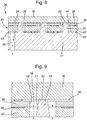
- Figure 8 is a close-up view of part of a substrate holder 20 according to an embodiment of the invention.
- the core body 21 comprises at least one gas supply passageway 38.
- the gas supply passageway 38 is configured to supply gas to the radial gap 39 between the radially outer surface 41 (shown in Figure 9 ) of at least one of the burls 22 and the electrostatic sheet 25 via a vertical gap 40 between the core body 21 and the electrostatic sheet 25.
- Figure 9 is a close-up view of the radial gap 39 between the radially outer surface 41 of the burl 22 and the wall 42 of the electrostatic sheet 25 that defines the holes 34 in the electrostatic sheet 25.
- the double ended arrows represent flow of gas.
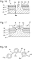
- the electrostatic shielding 45 By providing the electrostatic shielding 45, the possibility of undesirable electrical breakdown is reduced. This is particularly important when the size of the gaps between the electrode 26 and the burls 22 may not be well controlled because of manufacturing tolerances.
- the electrostatic shielding 45 helps to reduce electrical breakdown that may be caused due to charges flowing through the electrical insulator 44 or through the dielectric layers 27, 28.
- the electrode magnetic shielding 45 reduces the possibility of electrical breakdown as a result of surface conductivity of the bonding materials 29.
- the electrostatic shielding 45 reduces the possibility of undesirable electrostatic discharge across the gaps around the electrostatic sheet 25 that may be caused by materials entering those gaps.
Landscapes
- Physics & Mathematics (AREA)
- General Physics & Mathematics (AREA)
- Container, Conveyance, Adherence, Positioning, Of Wafer (AREA)
- Exposure And Positioning Against Photoresist Photosensitive Materials (AREA)
- Electron Beam Exposure (AREA)
- Turning (AREA)
- Polishing Bodies And Polishing Tools (AREA)
Priority Applications (9)
| Application Number | Priority Date | Filing Date | Title |
|---|---|---|---|
| EP20163373.2A EP3882700A1 (fr) | 2020-03-16 | 2020-03-16 | Porte-objet, outil et procédé de fabrication d'un porte-objet |
| US17/802,841 US12197139B2 (en) | 2020-03-16 | 2021-02-25 | Object holder, tool and method of manufacturing an object holder |
| JP2022550909A JP7661354B2 (ja) | 2020-03-16 | 2021-02-25 | オブジェクトホルダ、ツール、及びオブジェクトホルダの製造方法 |
| PCT/EP2021/054692 WO2021185552A1 (fr) | 2020-03-16 | 2021-02-25 | Porte-objet, outil et procédé de fabrication d'un porte-objet |
| KR1020227032168A KR20220154695A (ko) | 2020-03-16 | 2021-02-25 | 대상물 홀더, 툴 및 대상물 홀더를 제조하는 방법 |
| CN202180020908.7A CN115280243A (zh) | 2020-03-16 | 2021-02-25 | 物体保持器、工具和制造物体保持器的方法 |
| IL295864A IL295864A (en) | 2020-03-16 | 2021-02-25 | Object holder, tool and method of manufacturing an object holder |
| EP21706970.7A EP4121819A1 (fr) | 2020-03-16 | 2021-02-25 | Porte-objet, outil et procédé de fabrication d'un porte-objet |
| TW110109078A TWI900545B (zh) | 2020-03-16 | 2021-03-15 | 物件固持器及包含物件固持器之微影裝置 |
Applications Claiming Priority (1)
| Application Number | Priority Date | Filing Date | Title |
|---|---|---|---|
| EP20163373.2A EP3882700A1 (fr) | 2020-03-16 | 2020-03-16 | Porte-objet, outil et procédé de fabrication d'un porte-objet |
Publications (1)
| Publication Number | Publication Date |
|---|---|
| EP3882700A1 true EP3882700A1 (fr) | 2021-09-22 |
Family
ID=69844710
Family Applications (2)
| Application Number | Title | Priority Date | Filing Date |
|---|---|---|---|
| EP20163373.2A Withdrawn EP3882700A1 (fr) | 2020-03-16 | 2020-03-16 | Porte-objet, outil et procédé de fabrication d'un porte-objet |
| EP21706970.7A Pending EP4121819A1 (fr) | 2020-03-16 | 2021-02-25 | Porte-objet, outil et procédé de fabrication d'un porte-objet |
Family Applications After (1)
| Application Number | Title | Priority Date | Filing Date |
|---|---|---|---|
| EP21706970.7A Pending EP4121819A1 (fr) | 2020-03-16 | 2021-02-25 | Porte-objet, outil et procédé de fabrication d'un porte-objet |
Country Status (8)
| Country | Link |
|---|---|
| US (1) | US12197139B2 (fr) |
| EP (2) | EP3882700A1 (fr) |
| JP (1) | JP7661354B2 (fr) |
| KR (1) | KR20220154695A (fr) |
| CN (1) | CN115280243A (fr) |
| IL (1) | IL295864A (fr) |
| TW (1) | TWI900545B (fr) |
| WO (1) | WO2021185552A1 (fr) |
Cited By (3)
| Publication number | Priority date | Publication date | Assignee | Title |
|---|---|---|---|---|
| US11754929B2 (en) * | 2012-02-03 | 2023-09-12 | Asml Netherlands B.V. | Substrate holder and method of manufacturing a substrate holder |
| EP4372467A1 (fr) * | 2022-11-18 | 2024-05-22 | ASML Netherlands B.V. | Porte-objet et procédé de fabrication |
| US12560872B2 (en) | 2020-12-29 | 2026-02-24 | Asml Netherlands B.V. | Vacuum sheet bond fixturing and flexible burl applications for substrate tables |
Families Citing this family (3)
| Publication number | Priority date | Publication date | Assignee | Title |
|---|---|---|---|---|
| TW202243107A (zh) * | 2021-03-18 | 2022-11-01 | 荷蘭商Asml荷蘭公司 | 用於經改良疊對之夾具電極修改 |
| KR20260008748A (ko) * | 2023-05-12 | 2026-01-16 | 에이에스엠엘 네델란즈 비.브이. | 기판 지지체 |
| EP4481491A1 (fr) | 2023-06-20 | 2024-12-25 | ASML Netherlands B.V. | Procédé de fabrication d'une électrode pour un porte-objet |
Citations (9)
| Publication number | Priority date | Publication date | Assignee | Title |
|---|---|---|---|---|
| JP2002134599A (ja) * | 2000-10-24 | 2002-05-10 | Ngk Insulators Ltd | 静電吸着装置 |
| US20070103666A1 (en) * | 2005-11-08 | 2007-05-10 | Asml Netherlands B.V. | Lithographic apparatus and device manufacturing method |
| US20110222033A1 (en) | 2010-03-12 | 2011-09-15 | Asml Netherlands B.V. | Lithographic apparatus and method |
| US20130094009A1 (en) | 2011-10-14 | 2013-04-18 | Asml Netherlands B.V. | Substrate holder, lithographic apparatus, device manufacturing method, and method of manufacturing a substrate holder |
| US20130321788A1 (en) * | 2011-02-18 | 2013-12-05 | ASML Netherlands. B.V. | Lithographic Apparatus and Device Manufacturing Method |
| WO2014154428A2 (fr) | 2013-03-27 | 2014-10-02 | Asml Netherlands B.V. | Porte-objet, appareil lithographique, procédé de fabrication de dispositif et procédé de fabrication de porte-objet |
| US20150124234A1 (en) * | 2012-04-19 | 2015-05-07 | Asml Netherlands B.V. | Substrate holder, lithographic apparatus, and device manufacturing method |
| WO2015120923A1 (fr) | 2014-02-11 | 2015-08-20 | Asml Netherlands B.V. | Procédé de serrage d'articles et appareil lithographique |
| US20200013660A1 (en) * | 2018-07-06 | 2020-01-09 | Berliner Glas Kgaa Herbert Kubatz Gmbh & Co. | Electrostatic holding apparatus and method for its production |
Family Cites Families (10)
| Publication number | Priority date | Publication date | Assignee | Title |
|---|---|---|---|---|
| GB2106325A (en) * | 1981-09-14 | 1983-04-07 | Philips Electronic Associated | Electrostatic chuck |
| JP3469513B2 (ja) | 1999-08-24 | 2003-11-25 | 太平洋セメント株式会社 | 露光装置およびそれに用いられる支持部材 |
| JP5470601B2 (ja) | 2009-03-02 | 2014-04-16 | 新光電気工業株式会社 | 静電チャック |
| NL2008630A (en) | 2011-04-27 | 2012-10-30 | Asml Netherlands Bv | Substrate holder, lithographic apparatus, device manufacturing method, and method of manufacturing a substrate holder. |
| KR102203118B1 (ko) * | 2013-01-22 | 2021-01-15 | 에이에스엠엘 네델란즈 비.브이. | 정전기 클램프 |
| DE102014008029B4 (de) * | 2014-05-28 | 2023-05-17 | Asml Netherlands B.V. | Elektrostatische Haltevorrichtung mit einer Elektroden-Trägerscheibe und Verfahren zur Herstellung der Haltevorrichtung |
| CN110068991B (zh) * | 2014-10-23 | 2021-03-12 | Asml荷兰有限公司 | 用于光刻设备的支撑台和光刻设备 |
| DE102019108855B4 (de) * | 2019-04-04 | 2020-11-12 | Berliner Glas Kgaa Herbert Kubatz Gmbh & Co. | Elektrostatische Haltevorrichtung mit einer Schichtverbund-Elektrodeneinrichtung und Verfahren zu deren Herstellung |
| EP3923077A1 (fr) * | 2020-06-11 | 2021-12-15 | ASML Netherlands B.V. | Support d'objets, feuille électrostatique et procédé de fabrication d'une feuille électrostatique |
| WO2022078743A1 (fr) * | 2020-10-16 | 2022-04-21 | Asml Netherlands B.V. | Table d'objet, appareil à plateau, procédé de maintien et appareil lithographique |
-
2020
- 2020-03-16 EP EP20163373.2A patent/EP3882700A1/fr not_active Withdrawn
-
2021
- 2021-02-25 JP JP2022550909A patent/JP7661354B2/ja active Active
- 2021-02-25 US US17/802,841 patent/US12197139B2/en active Active
- 2021-02-25 KR KR1020227032168A patent/KR20220154695A/ko active Pending
- 2021-02-25 IL IL295864A patent/IL295864A/en unknown
- 2021-02-25 CN CN202180020908.7A patent/CN115280243A/zh active Pending
- 2021-02-25 WO PCT/EP2021/054692 patent/WO2021185552A1/fr not_active Ceased
- 2021-02-25 EP EP21706970.7A patent/EP4121819A1/fr active Pending
- 2021-03-15 TW TW110109078A patent/TWI900545B/zh active
Patent Citations (10)
| Publication number | Priority date | Publication date | Assignee | Title |
|---|---|---|---|---|
| JP2002134599A (ja) * | 2000-10-24 | 2002-05-10 | Ngk Insulators Ltd | 静電吸着装置 |
| US20070103666A1 (en) * | 2005-11-08 | 2007-05-10 | Asml Netherlands B.V. | Lithographic apparatus and device manufacturing method |
| US20110222033A1 (en) | 2010-03-12 | 2011-09-15 | Asml Netherlands B.V. | Lithographic apparatus and method |
| US20130321788A1 (en) * | 2011-02-18 | 2013-12-05 | ASML Netherlands. B.V. | Lithographic Apparatus and Device Manufacturing Method |
| US20130094009A1 (en) | 2011-10-14 | 2013-04-18 | Asml Netherlands B.V. | Substrate holder, lithographic apparatus, device manufacturing method, and method of manufacturing a substrate holder |
| US20150124234A1 (en) * | 2012-04-19 | 2015-05-07 | Asml Netherlands B.V. | Substrate holder, lithographic apparatus, and device manufacturing method |
| WO2014154428A2 (fr) | 2013-03-27 | 2014-10-02 | Asml Netherlands B.V. | Porte-objet, appareil lithographique, procédé de fabrication de dispositif et procédé de fabrication de porte-objet |
| US20160018744A1 (en) * | 2013-03-27 | 2016-01-21 | Asml Netherlands B.V. | Object holder, lithographic apparatus, device manufacturing method, and method of manufacturing an object holder |
| WO2015120923A1 (fr) | 2014-02-11 | 2015-08-20 | Asml Netherlands B.V. | Procédé de serrage d'articles et appareil lithographique |
| US20200013660A1 (en) * | 2018-07-06 | 2020-01-09 | Berliner Glas Kgaa Herbert Kubatz Gmbh & Co. | Electrostatic holding apparatus and method for its production |
Cited By (7)
| Publication number | Priority date | Publication date | Assignee | Title |
|---|---|---|---|---|
| US11754929B2 (en) * | 2012-02-03 | 2023-09-12 | Asml Netherlands B.V. | Substrate holder and method of manufacturing a substrate holder |
| US11960213B2 (en) | 2012-02-03 | 2024-04-16 | Asml Netherlands B.V. | Substrate holder, lithographic apparatus, device manufacturing method, and method of manufacturing a substrate holder |
| US12353139B2 (en) | 2012-02-03 | 2025-07-08 | Asml Netherlands B.V. | Substrate holder and method of manufacturing a substrate holder |
| US12366808B2 (en) | 2012-02-03 | 2025-07-22 | Asml Netherlands B.V. | Substrate holder, lithographic apparatus, device manufacturing method, and method of manufacturing a substrate holder |
| US12560872B2 (en) | 2020-12-29 | 2026-02-24 | Asml Netherlands B.V. | Vacuum sheet bond fixturing and flexible burl applications for substrate tables |
| EP4372467A1 (fr) * | 2022-11-18 | 2024-05-22 | ASML Netherlands B.V. | Porte-objet et procédé de fabrication |
| WO2024104782A1 (fr) * | 2022-11-18 | 2024-05-23 | Asml Netherlands B.V. | Porte-objet et procédé de fabrication |
Also Published As
| Publication number | Publication date |
|---|---|
| TW202138934A (zh) | 2021-10-16 |
| IL295864A (en) | 2022-10-01 |
| TWI900545B (zh) | 2025-10-11 |
| US12197139B2 (en) | 2025-01-14 |
| CN115280243A (zh) | 2022-11-01 |
| US20230105002A1 (en) | 2023-04-06 |
| JP2023519119A (ja) | 2023-05-10 |
| WO2021185552A1 (fr) | 2021-09-23 |
| EP4121819A1 (fr) | 2023-01-25 |
| JP7661354B2 (ja) | 2025-04-14 |
| KR20220154695A (ko) | 2022-11-22 |
Similar Documents
| Publication | Publication Date | Title |
|---|---|---|
| US12197139B2 (en) | Object holder, tool and method of manufacturing an object holder | |
| US12235592B2 (en) | Object holder, electrostatic sheet and method for making an electrostatic sheet | |
| KR101533014B1 (ko) | 정전기 클램프, 리소그래피 장치, 및 정전기 클램프를 제조하는 방법 | |
| CN105103052B (zh) | 物体保持装置及制造物体保持装置的方法 | |
| JP6497761B2 (ja) | 静電チャック用薄膜電極 | |
| KR20010100758A (ko) | 복수의 대전입자 빔 조정과 차폐된 대전입자 빔리소그래피를 위한 미세가공된 템플릿 | |
| JP2024529140A (ja) | 静電ホルダ、物体テーブル、およびリソグラフィ装置 | |
| TWI846973B (zh) | 靜電夾具、增強靜電夾具之方法及微影裝置 | |
| US12619165B2 (en) | Electrostatic holder, object table and lithographic apparatus | |
| EP4372467A1 (fr) | Porte-objet et procédé de fabrication | |
| EP4390541A1 (fr) | Table d'objets | |
| EP4134748A1 (fr) | Support électrostatique, table d'objet et appareil lithographique | |
| TW202435338A (zh) | 用於改變基板形狀的系統 | |
| CN117795430A (zh) | 静电保持器、载物台和光刻装置 |
Legal Events
| Date | Code | Title | Description |
|---|---|---|---|
| PUAI | Public reference made under article 153(3) epc to a published international application that has entered the european phase |
Free format text: ORIGINAL CODE: 0009012 |
|
| STAA | Information on the status of an ep patent application or granted ep patent |
Free format text: STATUS: THE APPLICATION HAS BEEN PUBLISHED |
|
| AK | Designated contracting states |
Kind code of ref document: A1 Designated state(s): AL AT BE BG CH CY CZ DE DK EE ES FI FR GB GR HR HU IE IS IT LI LT LU LV MC MK MT NL NO PL PT RO RS SE SI SK SM TR |
|
| STAA | Information on the status of an ep patent application or granted ep patent |
Free format text: STATUS: THE APPLICATION IS DEEMED TO BE WITHDRAWN |
|
| 18D | Application deemed to be withdrawn |
Effective date: 20220323 |