EP3882903A1 - Circuit de commande, module d'activation d'affichage à cristaux liquides et dispositif d'affichage à cristaux liquides - Google Patents
Circuit de commande, module d'activation d'affichage à cristaux liquides et dispositif d'affichage à cristaux liquides Download PDFInfo
- Publication number
- EP3882903A1 EP3882903A1 EP19883779.1A EP19883779A EP3882903A1 EP 3882903 A1 EP3882903 A1 EP 3882903A1 EP 19883779 A EP19883779 A EP 19883779A EP 3882903 A1 EP3882903 A1 EP 3882903A1
- Authority
- EP
- European Patent Office
- Prior art keywords
- field effect
- effect transistor
- type field
- input
- input end
- Prior art date
- Legal status (The legal status is an assumption and is not a legal conclusion. Google has not performed a legal analysis and makes no representation as to the accuracy of the status listed.)
- Granted
Links
Images


Classifications
-
- G—PHYSICS
- G09—EDUCATION; CRYPTOGRAPHY; DISPLAY; ADVERTISING; SEALS
- G09G—ARRANGEMENTS OR CIRCUITS FOR CONTROL OF INDICATING DEVICES USING STATIC MEANS TO PRESENT VARIABLE INFORMATION
- G09G3/00—Control arrangements or circuits, of interest only in connection with visual indicators other than cathode-ray tubes
- G09G3/20—Control arrangements or circuits, of interest only in connection with visual indicators other than cathode-ray tubes for presentation of an assembly of a number of characters, e.g. a page, by composing the assembly by combination of individual elements arranged in a matrix no fixed position being assigned to or needed to be assigned to the individual characters or partial characters
- G09G3/34—Control arrangements or circuits, of interest only in connection with visual indicators other than cathode-ray tubes for presentation of an assembly of a number of characters, e.g. a page, by composing the assembly by combination of individual elements arranged in a matrix no fixed position being assigned to or needed to be assigned to the individual characters or partial characters by control of light from an independent source
- G09G3/36—Control arrangements or circuits, of interest only in connection with visual indicators other than cathode-ray tubes for presentation of an assembly of a number of characters, e.g. a page, by composing the assembly by combination of individual elements arranged in a matrix no fixed position being assigned to or needed to be assigned to the individual characters or partial characters by control of light from an independent source using liquid crystals
- G09G3/3611—Control of matrices with row and column drivers
- G09G3/3696—Generation of voltages supplied to electrode drivers
-
- G—PHYSICS
- G09—EDUCATION; CRYPTOGRAPHY; DISPLAY; ADVERTISING; SEALS
- G09G—ARRANGEMENTS OR CIRCUITS FOR CONTROL OF INDICATING DEVICES USING STATIC MEANS TO PRESENT VARIABLE INFORMATION
- G09G3/00—Control arrangements or circuits, of interest only in connection with visual indicators other than cathode-ray tubes
- G09G3/20—Control arrangements or circuits, of interest only in connection with visual indicators other than cathode-ray tubes for presentation of an assembly of a number of characters, e.g. a page, by composing the assembly by combination of individual elements arranged in a matrix no fixed position being assigned to or needed to be assigned to the individual characters or partial characters
- G09G3/34—Control arrangements or circuits, of interest only in connection with visual indicators other than cathode-ray tubes for presentation of an assembly of a number of characters, e.g. a page, by composing the assembly by combination of individual elements arranged in a matrix no fixed position being assigned to or needed to be assigned to the individual characters or partial characters by control of light from an independent source
- G09G3/36—Control arrangements or circuits, of interest only in connection with visual indicators other than cathode-ray tubes for presentation of an assembly of a number of characters, e.g. a page, by composing the assembly by combination of individual elements arranged in a matrix no fixed position being assigned to or needed to be assigned to the individual characters or partial characters by control of light from an independent source using liquid crystals
-
- G—PHYSICS
- G06—COMPUTING OR CALCULATING; COUNTING
- G06F—ELECTRIC DIGITAL DATA PROCESSING
- G06F1/00—Details not covered by groups G06F3/00 - G06F13/00 and G06F21/00
- G06F1/26—Power supply means, e.g. regulation thereof
- G06F1/266—Arrangements to supply power to external peripherals either directly from the computer or under computer control, e.g. supply of power through the communication port, computer controlled power-strips
-
- H—ELECTRICITY
- H03—ELECTRONIC CIRCUITRY
- H03K—PULSE TECHNIQUE
- H03K17/00—Electronic switching or gating, i.e. not by contact-making and –breaking
- H03K17/296—Time-programme switches providing a choice of time-intervals for executing more than one switching action and automatically terminating their operation after the programme is completed
-
- G—PHYSICS
- G09—EDUCATION; CRYPTOGRAPHY; DISPLAY; ADVERTISING; SEALS
- G09G—ARRANGEMENTS OR CIRCUITS FOR CONTROL OF INDICATING DEVICES USING STATIC MEANS TO PRESENT VARIABLE INFORMATION
- G09G2300/00—Aspects of the constitution of display devices
- G09G2300/04—Structural and physical details of display devices
- G09G2300/0421—Structural details of the set of electrodes
- G09G2300/0426—Layout of electrodes and connections
-
- G—PHYSICS
- G09—EDUCATION; CRYPTOGRAPHY; DISPLAY; ADVERTISING; SEALS
- G09G—ARRANGEMENTS OR CIRCUITS FOR CONTROL OF INDICATING DEVICES USING STATIC MEANS TO PRESENT VARIABLE INFORMATION
- G09G2310/00—Command of the display device
- G09G2310/06—Details of flat display driving waveforms
- G09G2310/066—Waveforms comprising a gently increasing or decreasing portion, e.g. ramp
-
- G—PHYSICS
- G09—EDUCATION; CRYPTOGRAPHY; DISPLAY; ADVERTISING; SEALS
- G09G—ARRANGEMENTS OR CIRCUITS FOR CONTROL OF INDICATING DEVICES USING STATIC MEANS TO PRESENT VARIABLE INFORMATION
- G09G2330/00—Aspects of power supply; Aspects of display protection and defect management
- G09G2330/02—Details of power systems and of start or stop of display operation
-
- G—PHYSICS
- G09—EDUCATION; CRYPTOGRAPHY; DISPLAY; ADVERTISING; SEALS
- G09G—ARRANGEMENTS OR CIRCUITS FOR CONTROL OF INDICATING DEVICES USING STATIC MEANS TO PRESENT VARIABLE INFORMATION
- G09G2330/00—Aspects of power supply; Aspects of display protection and defect management
- G09G2330/02—Details of power systems and of start or stop of display operation
- G09G2330/025—Reduction of instantaneous peaks of current
-
- G—PHYSICS
- G09—EDUCATION; CRYPTOGRAPHY; DISPLAY; ADVERTISING; SEALS
- G09G—ARRANGEMENTS OR CIRCUITS FOR CONTROL OF INDICATING DEVICES USING STATIC MEANS TO PRESENT VARIABLE INFORMATION
- G09G2330/00—Aspects of power supply; Aspects of display protection and defect management
- G09G2330/02—Details of power systems and of start or stop of display operation
- G09G2330/026—Arrangements or methods related to booting a display
-
- G—PHYSICS
- G09—EDUCATION; CRYPTOGRAPHY; DISPLAY; ADVERTISING; SEALS
- G09G—ARRANGEMENTS OR CIRCUITS FOR CONTROL OF INDICATING DEVICES USING STATIC MEANS TO PRESENT VARIABLE INFORMATION
- G09G2330/00—Aspects of power supply; Aspects of display protection and defect management
- G09G2330/02—Details of power systems and of start or stop of display operation
- G09G2330/027—Arrangements or methods related to powering off a display
-
- G—PHYSICS
- G09—EDUCATION; CRYPTOGRAPHY; DISPLAY; ADVERTISING; SEALS
- G09G—ARRANGEMENTS OR CIRCUITS FOR CONTROL OF INDICATING DEVICES USING STATIC MEANS TO PRESENT VARIABLE INFORMATION
- G09G2330/00—Aspects of power supply; Aspects of display protection and defect management
- G09G2330/02—Details of power systems and of start or stop of display operation
- G09G2330/028—Generation of voltages supplied to electrode drivers in a matrix display other than LCD
-
- G—PHYSICS
- G09—EDUCATION; CRYPTOGRAPHY; DISPLAY; ADVERTISING; SEALS
- G09G—ARRANGEMENTS OR CIRCUITS FOR CONTROL OF INDICATING DEVICES USING STATIC MEANS TO PRESENT VARIABLE INFORMATION
- G09G2330/00—Aspects of power supply; Aspects of display protection and defect management
- G09G2330/04—Display protection
Definitions
- the present disclosure relates to the field of communications technologies, and in particular, to a control circuit, a liquid crystal display drive module, and a liquid crystal display apparatus.
- An external power supply of a drive chip of a liquid crystal display drive module mainly includes a VDDI signal, an AVDD signal, and an AVEE signal during power supply.
- the VDDI signal is powered on earlier than the AVDD signal and the AVEE signal, and the VDDI signal is powered off later than the AVDD signal and the AVEE signal.
- the three work together to make the liquid crystal display drive module work normally.
- the AVDD signal and the AVEE signal may be powered on earlier than the VDDI signal, or the AVDD signal and the AVEE signal may be powered off later than the VDDI signal, which has a high probability of causing damage to the drive chip.
- Some embodiments of the present disclosure provide a control circuit, a liquid crystal display drive module, and a liquid crystal display apparatus, to resolve the problem of a high probability of causing damage to the drive chip under abnormal circumstances.
- some embodiments of the present disclosure provide a control circuit, configured to control an on/off time sequence of multiple power source signals inputted to a drive chip of a display module, where the control circuit includes a first input end and a second input end that separately receive different external power source signals, and the control circuit sequentially controls the first input end and the second input end to input a power source signal to the drive chip, and sequentially controls the second input end and the first input end to power off.
- some embodiments of the present disclosure further provide a liquid crystal display drive module, including a drive chip, where the liquid crystal display drive module further includes the foregoing control circuit.
- some embodiments of the present disclosure further provide a liquid crystal display apparatus, including the foregoing liquid crystal display drive module.
- a control circuit in some embodiments of the present disclosure is configured to control an on/off time sequence of multiple power source signals inputted to a drive chip of a display module, where the control circuit includes a first input end and a second input end that separately receive different external power source signals, and the control circuit sequentially controls the first input end and the second input end to input a power source signal to the drive chip, and sequentially controls the second input end and the first input end to power off.
- the control circuit includes a first input end and a second input end that separately receive different external power source signals, and the control circuit sequentially controls the first input end and the second input end to input a power source signal to the drive chip, and sequentially controls the second input end and the first input end to power off.
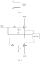
- FIG. 1 is a schematic structural diagram of a control circuit according to some embodiments of the present disclosure.
- the control circuit is configured to control an on/off time sequence of multiple external power source signals inputted to a drive chip of a display module.
- the control circuit includes a first input end 101 and a second input end 102 that separately receive different external power source signals, and the control circuit sequentially controls the first input end 101 and the second input end 102 to input a power source signal to the drive chip, and sequentially controls the second input end 102 and the first input end 101 to power off.
- the first input end 101 may be a VDDI input end
- the second input end 102 may be an AVDD input end or an AVEE input end.
- the VDDI signal can be inputted to the drive chip earlier than the AVDD signal or the AVEE signal
- the AVDD signal or the AVEE signal can be powered off earlier than the VDDI signal.
- the control circuit includes a capacitor, which sequentially controls the second input end and the first input end to power off.
- the normal time sequence between different power source signals can be ensured as much as possible, to reduce the probability of damaging the drive chip.
- the second input end includes a second input sub-end and a third input sub-end, the second input sub-end and the third input sub-end separately receive different external power source signals, and the control circuit sequentially controls the first input end, the second input sub-end, and the third input sub-end to input a power source signal to the drive chip, and sequentially controls the third input sub-end, the second input sub-end, and the first input end to power off.
- the second input end includes the second input sub-end and the third input sub-end, the second input sub-end and the third input sub-end separately receive different external power source signals
- the control circuit sequentially controls the first input end, the second input sub-end, and the third input sub-end to input a power source signal to the drive chip, and sequentially controls the third input sub-end, the second input sub-end, and the first input end to power off.
- the first input end is a VDDI input end
- the second input sub-end is an AVEE input end
- the third input sub-end is an AVDD input end.
- the first input end is a VDDI input end
- the second input sub-end is an AVDD input end
- the third input sub-end is an AVEE input end.
- the first input end is a VDDI input end
- the second input sub-end is an AVEE input end
- the third input sub-end is an AVDD input end
- the first input end is the VDDI input end
- the second input sub-end is the AVDD input end
- the third input sub-end is the AVEE input end
- the normal time sequence of the AVDD signal, the AVEE signal, and the VDDI signal is controlled, to reduce the probability of damaging the drive chip caused by a latch high current inside.
- the first input end is a VDDI input end
- the second input sub-end is an AVEE input end
- the third input sub-end is an AVDD input end
- the control circuit includes:
- the position of the second electrode of the N-type field effect transistor M1 that is connected to the drive chip is different from the position of the second electrode of the P-type field effect transistor M2 that is connected to the drive chip.
- the first electrode and the second electrode of the N-type field effect transistor M1 or the P-type field effect transistor M2 can be the source electrode and the drain electrode respectively, or can be the drain electrode and the source electrode respectively.
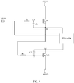
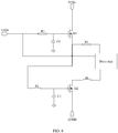
- FIG. 2 and FIG. 3 are both schematic structural diagrams of control circuits according to some embodiments of the present disclosure.
- the VDDI signal is used as a gate control signal of the N-type field effect transistor M1.
- the VDDI voltage reaches, for example, 1.8V
- the VDDI signal first charges the first capacitor C1 through the first resistor R1.
- the AVEE signal starts to input through the N-type field effect transistor M1.
- the inputted AVEE signal is divided into multiple channels. One channel of inputted AVEE signal enters the boost circuit of the drive chip.
- Another channel of inputted AVEE signal charges the second capacitor C2 through the second resistor R2.
- the second capacitor C2 is charged for a certain period of time and reaches the power-on voltage of the P-type field effect transistor M2
- the AVDD signal is inputted through the P-type field effect transistor M2. Therefore, even if the external power supply is abnormal and the AVDD signal or the AVEE signal supplies power earlier than the VDDI signal, the AVDD signal or the AVEE signal cannot be inputted into the drive chip earlier than the VDDI signal.
- the voltage of the VDDI signal is 1.8V
- the first resistor R1 is 10K ohm
- the first capacitor C1 is 4.7 ⁇ F.
- the voltage of the AVEE signal is - 5.5V
- the second resistor R2 is 1K ohm
- the second capacitor C2 is 1 ⁇ F
- the N-type field effect transistor M1 is turned on, the AVEE signal is powered on, then the second capacitor C2 is charged, and the AVDD signal is powered on for input.
- the VDDI signal is first inputted among the three channels of power supply, so that the drive chip works normally.
- the AVEE signal is inputted.
- the AVDD signal is inputted, so that the boost circuit of the drive chip works under the drive of the AVEE signal and the AVDD signal.
- the first capacitor C1 and the second capacitor C2 are fully charged in a power-on state.
- the power supply of the VDDI, the AVDD, and the AVEE is disconnected, the AVDD signal exists because of another capacitor and a parasitic capacitor. After the capacitor discharges for a period of time, there is no input and power-off occurs. Because the first capacitor C1 and the second capacitor C2 store more power, they continue to input power for a longer period of time.
- R1C1 can be set to be greater than R2C2 to ensure that the continuous input time of the VDDI signal is longer than the continuous input time of the AVEE signal.
- the expected state in which the AVDD signal is powered off first, the AVEE signal is powered off next, and the VDDI signal is powered off last can be achieved.
- the AVDD signal is turned off first, then the AVEE signal is turned off, and finally the VDDI signal is turned off.
- the circuit In the circuit structure shown in FIG. 2 , no matter how the external voltage abnormally provides power supply and abnormally powers off, the circuit is disposed, so that power supply can be provided according to a required power supply sequence that is set or power-off is implemented according to a desired sequence.
- a second end of the first capacitor C1 is connected to the second electrode of the N-type field effect transistor M1, and a second end of the second capacitor C2 is connected to the second electrode of the P-type field effect transistor M2.
- the VDDI signal charges the first capacitor C1 and turns on the N-type field effect transistor M1
- the AVEE signal (generally - 5.5V) is inputted to the node N1, which increases the voltage difference between the node N3 and the node N1 and accelerates the charging speed of the first capacitor C1.
- the voltage differences between the gate electrode and the source electrode and between the gate electrode and the drain electrode of the N-type field effect transistor M1 increase, so that the speed at which the current of the AVEE signal passes through the N-type field effect transistor M1 is faster, that is, the speed at which the AVEE signal reaches a preset value -5.5V from 0V is faster.
- the voltage difference between the node N4 and the node N2 increases rapidly, which improves the power-on speed of the AVDD signal.
- the AVDD signal and the AVEE signal power on rapidly to reach the predetermined voltage, which can reduce the probability that the boost circuit of the drive chip has logic confusion and consequently a latch high current burns the drive chip. Therefore, the power-on process of power supply of the boost circuit is optimized.
- the first input end is a VDDI input end
- the second input sub-end is an AVDD input end
- the third input sub-end is an AVEE input end
- the control circuit includes:
- FIG. 4 is a schematic structural diagram of a control circuit according to some embodiments of the present disclosure.
- the second end of the third capacitor C3 is grounded, and the second end of the fourth capacitor C4 is grounded.
- the VDDI signal charges the third capacitor C3.
- the third capacitor C3 may start to reach the threshold voltage to turn on the first N-type field effect transistor M3.
- the first N-type field effect transistor M3 is turned on.
- the AVDD signal is inputted through the first N-type field effect transistor M3.
- One channel of the AVDD signal enters the boost circuit of the drive chip, and the other channel of the AVDD signal charges the fourth capacitor C4 through the fourth resistor R4.
- the second N-type field effect transistor M4 is turned on, and the AVEE signal can be inputted into the drive chip. This ensures a power-on sequence in which the VDDI signal is powered on first, then the AVDD signal is powered on, and finally the AVEE signal is powered on.
- control circuit includes:
- the position of the second electrode of the third N-type field effect transistor M5 that is connected to the drive chip is different from the position of the second electrode of the fourth N-type field effect transistor M6 that is connected to the drive chip.
- the first electrode and the second electrode of the third N-type field effect transistor M5 or the fourth N-type field effect transistor M6 can be the source electrode and the drain electrode respectively, or can be the drain electrode and the source electrode respectively.
- the first target field effect transistor is the third N-type field effect transistor M5
- the second target field effect transistor is the fourth N-type field effect transistor M6.
- the first target field effect transistor is the fourth N-type field effect transistor M6
- the second target field effect transistor is the third N-type field effect transistor M5.
- the selecting circuit can include different capacitors to control power-on and power-off time sequences of the AVDD signal and the AVEE signal.
- the second input sub-end is an AVEE input end
- the third input sub-end is an AVDD input end.
- the second input sub-end is an AVDD input end
- the third input sub-end is an AVEE input end.
- FIG. 5 is a schematic structural diagram of a control circuit according to some embodiments of the present disclosure.
- the drive signal is outputted.
- the third N-type field effect transistor M5 and the fourth N-type field effect transistor M6 are turned on successively to control the AVDD signal to be inputted first and the AVEE signal to be inputted next.
- This can be fixed in the drive chip by programming in advance.
- the drive chip can be programmed to determine the power-on sequence of the AVDD signal and the AVEE signal, and the selecting circuit outputs the control signal in a corresponding sequence. In this way, the input of the AVDD signal and the AVEE signal can be controlled flexibly by programming.
- thermosensitive resistor is connected on the paths of the AVEE input end and the drive chip in series. and/or a thermosensitive resistor is connected on the paths of the AVDD input end and the drive chip in series.
- thermosensitive resistor is connected in series.
- the boost circuit of the drive chip has a latch large current
- the increase of the current causes the thermosensitive resistor to heat and increase in resistance, which reduces the current that flows, thus protecting the drive chip.
- FIG. 6 is a schematic structural diagram of a control circuit according to some embodiments of the present disclosure.
- a thermosensitive resistor R5 is connected on the paths of the AVEE input end and the drive chip in series
- a thermosensitive resistor R6 is connected on the paths of the AVDD input end and the drive chip in series.
- a thyristor may also be used to control the current of power supply.
- the resistor, the thermosensive resistor, and the capacitor in the circuit can be disposed on an external circuit board or integrated into the drive chip.
- a control circuit in some embodiments of the present disclosure is configured to control an on/off time sequence of multiple power source signals inputted to a drive chip of a display module, where the control circuit includes a first input end 101 and a second input end 102 that separately receive different external power source signals, and the control circuit sequentially controls the first input end 101 and the second input end 102 to input a power source signal to the drive chip, and sequentially controls the second input end 102 and the first input end 101 to power off.
- the control circuit includes a first input end 101 and a second input end 102 that separately receive different external power source signals, and the control circuit sequentially controls the first input end 101 and the second input end 102 to input a power source signal to the drive chip, and sequentially controls the second input end 102 and the first input end 101 to power off.
- Some embodiments of the present disclosure further provide a liquid crystal display drive module, including a drive chip, where the liquid crystal display drive module further includes the foregoing control circuit.
- Some embodiments of the present disclosure further provide a liquid crystal display apparatus, including the foregoing liquid crystal display drive module.
- the liquid crystal display apparatus may be a mobile phone, a tablet personal computer (Tablet Personal Computer), a laptop computer (Laptop Computer), a personal digital assistant (Personal Digital Assistant, PDA), a mobile internet device (Mobile Internet Device, MID), a wearable device (Wearable Device), or the like.
Landscapes
- Engineering & Computer Science (AREA)
- Theoretical Computer Science (AREA)
- Computer Hardware Design (AREA)
- Physics & Mathematics (AREA)
- General Physics & Mathematics (AREA)
- Chemical & Material Sciences (AREA)
- Crystallography & Structural Chemistry (AREA)
- General Engineering & Computer Science (AREA)
- Control Of Indicators Other Than Cathode Ray Tubes (AREA)
- Electronic Switches (AREA)
- Liquid Crystal Display Device Control (AREA)
- Transforming Electric Information Into Light Information (AREA)
- Liquid Crystal (AREA)
Applications Claiming Priority (2)
| Application Number | Priority Date | Filing Date | Title |
|---|---|---|---|
| CN201811353013.1A CN109192177B (zh) | 2018-11-14 | 2018-11-14 | 一种控制电路、液晶显示驱动模组及液晶显示装置 |
| PCT/CN2019/116588 WO2020098569A1 (fr) | 2018-11-14 | 2019-11-08 | Circuit de commande, module d'activation d'affichage à cristaux liquides et dispositif d'affichage à cristaux liquides |
Publications (3)
| Publication Number | Publication Date |
|---|---|
| EP3882903A1 true EP3882903A1 (fr) | 2021-09-22 |
| EP3882903A4 EP3882903A4 (fr) | 2022-01-05 |
| EP3882903B1 EP3882903B1 (fr) | 2025-12-03 |
Family
ID=64939088
Family Applications (1)
| Application Number | Title | Priority Date | Filing Date |
|---|---|---|---|
| EP19883779.1A Active EP3882903B1 (fr) | 2018-11-14 | 2019-11-08 | Circuit de commande, module d'activation d'affichage à cristaux liquides et dispositif d'affichage à cristaux liquides |
Country Status (7)
| Country | Link |
|---|---|
| US (1) | US11462190B2 (fr) |
| EP (1) | EP3882903B1 (fr) |
| JP (1) | JP7315671B2 (fr) |
| KR (1) | KR102552625B1 (fr) |
| CN (1) | CN109192177B (fr) |
| ES (1) | ES3058058T3 (fr) |
| WO (1) | WO2020098569A1 (fr) |
Families Citing this family (5)
| Publication number | Priority date | Publication date | Assignee | Title |
|---|---|---|---|---|
| CN109192177B (zh) | 2018-11-14 | 2023-03-17 | 维沃移动通信有限公司 | 一种控制电路、液晶显示驱动模组及液晶显示装置 |
| TWI799244B (zh) * | 2022-04-26 | 2023-04-11 | 友達光電股份有限公司 | 畫素電路及其關機供電順序的供電方法 |
| CN116700106B (zh) * | 2023-06-30 | 2024-04-19 | 合肥申威睿思信息科技有限公司 | 一种上下电时序控制电路和方法 |
| KR20250014471A (ko) * | 2023-07-20 | 2025-02-03 | 삼성전자주식회사 | 디스플레이 장치 그 구동 방법 |
| CN118157643B (zh) * | 2024-01-26 | 2025-11-14 | 惠科股份有限公司 | 微流控有源矩阵驱动电路和微流控装置 |
Family Cites Families (27)
| Publication number | Priority date | Publication date | Assignee | Title |
|---|---|---|---|---|
| JPS517522A (ja) * | 1974-07-09 | 1976-01-21 | Zetsuto Kogyo Kk | Kanshinbensochi |
| JPH05107522A (ja) * | 1991-07-11 | 1993-04-30 | Sony Corp | 液晶表示装置 |
| JP2005043435A (ja) * | 2003-07-23 | 2005-02-17 | Renesas Technology Corp | 表示駆動制御装置とその駆動方法及び電子機器並びに半導体集積回路 |
| KR20050034259A (ko) * | 2003-10-09 | 2005-04-14 | 엘지전자 주식회사 | 돌입 전류 방지 회로 |
| JP3922381B2 (ja) * | 2004-10-14 | 2007-05-30 | 船井電機株式会社 | 液晶テレビジョン受像機 |
| JP2007065135A (ja) * | 2005-08-30 | 2007-03-15 | Sanyo Epson Imaging Devices Corp | 液晶表示装置 |
| JP2007065136A (ja) * | 2005-08-30 | 2007-03-15 | Sanyo Epson Imaging Devices Corp | 液晶表示装置 |
| JP4161226B2 (ja) * | 2006-04-12 | 2008-10-08 | 船井電機株式会社 | 液晶テレビジョン装置 |
| TW200742971A (en) * | 2006-05-15 | 2007-11-16 | Beyond Innovation Tech Co Ltd | Power supply and switch apparatus thereof |
| CN200983156Y (zh) | 2006-12-15 | 2007-11-28 | 鸿富锦精密工业(深圳)有限公司 | 时序控制电路 |
| CN201017211Y (zh) * | 2007-03-16 | 2008-02-06 | 谢红卫 | 节能型电源控制器 |
| KR20080102039A (ko) * | 2007-05-17 | 2008-11-24 | 삼성전자주식회사 | 액정 표시 장치 및 이의 구동 방법 |
| CN100592374C (zh) * | 2007-06-15 | 2010-02-24 | 群康科技(深圳)有限公司 | 液晶显示装置及其电源时序控制电路 |
| CN101377907B (zh) * | 2007-08-31 | 2013-07-17 | 北京京东方光电科技有限公司 | 模拟电源信号延时装置 |
| CN201860306U (zh) * | 2010-10-29 | 2011-06-08 | 珠海市鑫和电器有限公司 | 一种时序控制电路 |
| CN202076999U (zh) * | 2011-04-28 | 2011-12-14 | 惠州Tcl移动通信有限公司 | 一种电源控制管理电路 |
| US9360539B2 (en) | 2012-08-29 | 2016-06-07 | National Institute Of Health (Nih), U.S. Dept. Of Health And Human Services (Dhhs), U.S. Government | System and method for perfusion and diffusion MR imaging |
| TWI464717B (zh) * | 2012-09-03 | 2014-12-11 | Hon Hai Prec Ind Co Ltd | 時序控制電路及使用其的電子裝置 |
| US9198254B2 (en) * | 2012-12-14 | 2015-11-24 | Shenzhen China Star Optoelectronics Technology Co., Ltd | LED backlight driving circuit and LCD device |
| JP5932738B2 (ja) * | 2013-09-02 | 2016-06-08 | キヤノン株式会社 | 電子機器及び電子機器の制御部への電力制御方法 |
| KR102215086B1 (ko) * | 2014-09-16 | 2021-02-15 | 삼성디스플레이 주식회사 | 전압 공급 회로 및 이를 포함하는 디스플레이 장치 |
| CN204539105U (zh) * | 2015-04-27 | 2015-08-05 | 山东亚华电子有限公司 | 上电和断电时序控制电路 |
| CN104795038B (zh) * | 2015-04-29 | 2017-12-05 | 南京中电熊猫液晶显示科技有限公司 | 一种液晶面板的驱动电路 |
| CN107817699B (zh) * | 2016-09-12 | 2023-11-17 | 高创(苏州)电子有限公司 | 控制电路、控制方法和电子设备 |
| TWI637367B (zh) * | 2016-09-12 | 2018-10-01 | 瑞鼎科技股份有限公司 | 閘極驅動器 |
| CN106847215B (zh) * | 2017-03-02 | 2019-07-26 | 昆山龙腾光电有限公司 | 显示装置 |
| CN109192177B (zh) * | 2018-11-14 | 2023-03-17 | 维沃移动通信有限公司 | 一种控制电路、液晶显示驱动模组及液晶显示装置 |
-
2018
- 2018-11-14 CN CN201811353013.1A patent/CN109192177B/zh active Active
-
2019
- 2019-11-08 KR KR1020217017563A patent/KR102552625B1/ko active Active
- 2019-11-08 JP JP2021525802A patent/JP7315671B2/ja active Active
- 2019-11-08 ES ES19883779T patent/ES3058058T3/es active Active
- 2019-11-08 WO PCT/CN2019/116588 patent/WO2020098569A1/fr not_active Ceased
- 2019-11-08 EP EP19883779.1A patent/EP3882903B1/fr active Active
-
2021
- 2021-05-13 US US17/319,404 patent/US11462190B2/en active Active
Also Published As
| Publication number | Publication date |
|---|---|
| JP2022507305A (ja) | 2022-01-18 |
| KR20210091225A (ko) | 2021-07-21 |
| CN109192177B (zh) | 2023-03-17 |
| US11462190B2 (en) | 2022-10-04 |
| WO2020098569A1 (fr) | 2020-05-22 |
| JP7315671B2 (ja) | 2023-07-26 |
| CN109192177A (zh) | 2019-01-11 |
| WO2020098569A8 (fr) | 2021-06-03 |
| ES3058058T3 (en) | 2026-03-06 |
| KR102552625B1 (ko) | 2023-07-05 |
| EP3882903A4 (fr) | 2022-01-05 |
| EP3882903B1 (fr) | 2025-12-03 |
| US20210264869A1 (en) | 2021-08-26 |
Similar Documents
| Publication | Publication Date | Title |
|---|---|---|
| US11462190B2 (en) | Control circuit, liquid crystal display drive module, and liquid crystal display apparatus | |
| US10229634B2 (en) | Level shifting unit, level shifting circuit, method for driving the level shifting circuit, gate driving circuit and display device | |
| US10380935B2 (en) | Thin film transistor, array substrate, display panel and display device | |
| JP6420056B2 (ja) | 携帯端末及び表示パネルドライバ | |
| US10587266B2 (en) | Level-shift circuit and display device | |
| US10614770B2 (en) | Driving module for display device | |
| EP3553768B1 (fr) | Procédé et appareil de commande de source d'alimentation électrique d'écran d'affichage, support d'informations et dispositif électronique | |
| EP3427135B1 (fr) | Circuit de réinitialisation, unité registre à décalage et circuit de balayage de grille | |
| US9570941B2 (en) | Autonomous power supply | |
| US9383794B2 (en) | Integrated circuit with multi-voltage input/output (I/O) cells | |
| US9721524B2 (en) | Power supply circuit, display panel driver and display device incorporating the same | |
| KR102307678B1 (ko) | 표시장치의 발광제어신호 구동부 및 이의 구동방법, 유기발광 표시장치 | |
| US20160190928A1 (en) | Voltage Division Circuit, Circuit for Controlling Operation Voltage and Storage Device | |
| US9608476B2 (en) | Charging system and charging method thereof | |
| EP2479633B1 (fr) | Régulateur de tension avec circuit de préchargement | |
| US10037733B2 (en) | Enable signal generation circuit, power conversion circuit and display device | |
| CN109036302B (zh) | 液晶显示器 | |
| JP5750326B2 (ja) | 電子機器の保護回路 | |
| CN110442220B (zh) | 一种用于usb-c接口设备的电源控制装置和方法 | |
| EP3968491A1 (fr) | Circuit de charge, puce de charge, terminal mobile, et système de charge | |
| KR102157547B1 (ko) | 쉬프트 레지스터 | |
| JP2012186990A (ja) | 半導体装置、スイッチングレギュレータ、テレビ | |
| CN114172140B (zh) | 静电防护电路、电路板组件及液晶显示装置 | |
| CN113920936B (zh) | 一种信号监测电路、显示控制电路及显示装置 | |
| US9733683B2 (en) | Motherboard and electronic device using the same |
Legal Events
| Date | Code | Title | Description |
|---|---|---|---|
| STAA | Information on the status of an ep patent application or granted ep patent |
Free format text: STATUS: THE INTERNATIONAL PUBLICATION HAS BEEN MADE |
|
| PUAI | Public reference made under article 153(3) epc to a published international application that has entered the european phase |
Free format text: ORIGINAL CODE: 0009012 |
|
| STAA | Information on the status of an ep patent application or granted ep patent |
Free format text: STATUS: REQUEST FOR EXAMINATION WAS MADE |
|
| 17P | Request for examination filed |
Effective date: 20210609 |
|
| AK | Designated contracting states |
Kind code of ref document: A1 Designated state(s): AL AT BE BG CH CY CZ DE DK EE ES FI FR GB GR HR HU IE IS IT LI LT LU LV MC MK MT NL NO PL PT RO RS SE SI SK SM TR |
|
| A4 | Supplementary search report drawn up and despatched |
Effective date: 20211203 |
|
| RIC1 | Information provided on ipc code assigned before grant |
Ipc: G06F 1/26 20060101ALI20211129BHEP Ipc: H03K 17/296 20060101ALI20211129BHEP Ipc: G09G 3/36 20060101AFI20211129BHEP |
|
| DAV | Request for validation of the european patent (deleted) | ||
| DAX | Request for extension of the european patent (deleted) | ||
| STAA | Information on the status of an ep patent application or granted ep patent |
Free format text: STATUS: EXAMINATION IS IN PROGRESS |
|
| 17Q | First examination report despatched |
Effective date: 20230526 |
|
| GRAP | Despatch of communication of intention to grant a patent |
Free format text: ORIGINAL CODE: EPIDOSNIGR1 |
|
| STAA | Information on the status of an ep patent application or granted ep patent |
Free format text: STATUS: GRANT OF PATENT IS INTENDED |
|
| INTG | Intention to grant announced |
Effective date: 20250905 |
|
| GRAS | Grant fee paid |
Free format text: ORIGINAL CODE: EPIDOSNIGR3 |
|
| GRAA | (expected) grant |
Free format text: ORIGINAL CODE: 0009210 |
|
| STAA | Information on the status of an ep patent application or granted ep patent |
Free format text: STATUS: THE PATENT HAS BEEN GRANTED |
|
| AK | Designated contracting states |
Kind code of ref document: B1 Designated state(s): AL AT BE BG CH CY CZ DE DK EE ES FI FR GB GR HR HU IE IS IT LI LT LU LV MC MK MT NL NO PL PT RO RS SE SI SK SM TR |
|
| REG | Reference to a national code |
Ref country code: CH Ref legal event code: F10 Free format text: ST27 STATUS EVENT CODE: U-0-0-F10-F00 (AS PROVIDED BY THE NATIONAL OFFICE) Effective date: 20251203 Ref country code: GB Ref legal event code: FG4D |
|
| REG | Reference to a national code |
Ref country code: DE Ref legal event code: R096 Ref document number: 602019078884 Country of ref document: DE |
|
| REG | Reference to a national code |
Ref country code: IE Ref legal event code: FG4D |
|
| REG | Reference to a national code |
Ref country code: NL Ref legal event code: FP |
|
| REG | Reference to a national code |
Ref country code: ES Ref legal event code: FG2A Ref document number: 3058058 Country of ref document: ES Kind code of ref document: T3 Effective date: 20260306 |
|
| REG | Reference to a national code |
Ref country code: LT Ref legal event code: MG9D |
|
| PG25 | Lapsed in a contracting state [announced via postgrant information from national office to epo] |
Ref country code: NO Free format text: LAPSE BECAUSE OF FAILURE TO SUBMIT A TRANSLATION OF THE DESCRIPTION OR TO PAY THE FEE WITHIN THE PRESCRIBED TIME-LIMIT Effective date: 20260303 |
|
| PG25 | Lapsed in a contracting state [announced via postgrant information from national office to epo] |
Ref country code: FI Free format text: LAPSE BECAUSE OF FAILURE TO SUBMIT A TRANSLATION OF THE DESCRIPTION OR TO PAY THE FEE WITHIN THE PRESCRIBED TIME-LIMIT Effective date: 20251203 Ref country code: HR Free format text: LAPSE BECAUSE OF FAILURE TO SUBMIT A TRANSLATION OF THE DESCRIPTION OR TO PAY THE FEE WITHIN THE PRESCRIBED TIME-LIMIT Effective date: 20251203 |
|
| PG25 | Lapsed in a contracting state [announced via postgrant information from national office to epo] |
Ref country code: RS Free format text: LAPSE BECAUSE OF FAILURE TO SUBMIT A TRANSLATION OF THE DESCRIPTION OR TO PAY THE FEE WITHIN THE PRESCRIBED TIME-LIMIT Effective date: 20260303 |
|
| PG25 | Lapsed in a contracting state [announced via postgrant information from national office to epo] |
Ref country code: PL Free format text: LAPSE BECAUSE OF FAILURE TO SUBMIT A TRANSLATION OF THE DESCRIPTION OR TO PAY THE FEE WITHIN THE PRESCRIBED TIME-LIMIT Effective date: 20251203 |
|
| PG25 | Lapsed in a contracting state [announced via postgrant information from national office to epo] |
Ref country code: LV Free format text: LAPSE BECAUSE OF FAILURE TO SUBMIT A TRANSLATION OF THE DESCRIPTION OR TO PAY THE FEE WITHIN THE PRESCRIBED TIME-LIMIT Effective date: 20251203 |