EP3883233B1 - Anzeigebildschirmanordnung und elektronische vorrichtung - Google Patents
Anzeigebildschirmanordnung und elektronische vorrichtung Download PDFInfo
- Publication number
- EP3883233B1 EP3883233B1 EP19890587.9A EP19890587A EP3883233B1 EP 3883233 B1 EP3883233 B1 EP 3883233B1 EP 19890587 A EP19890587 A EP 19890587A EP 3883233 B1 EP3883233 B1 EP 3883233B1
- Authority
- EP
- European Patent Office
- Prior art keywords
- display
- display screen
- laminate
- screen assembly
- image sensors
- Prior art date
- Legal status (The legal status is an assumption and is not a legal conclusion. Google has not performed a legal analysis and makes no representation as to the accuracy of the status listed.)
- Active
Links
Images




Classifications
-
- H—ELECTRICITY
- H04—ELECTRIC COMMUNICATION TECHNIQUE
- H04M—TELEPHONIC COMMUNICATION
- H04M1/00—Substation equipment, e.g. for use by subscribers
- H04M1/02—Constructional features of telephone sets
- H04M1/0202—Portable telephone sets, e.g. cordless phones, mobile phones or bar type handsets
- H04M1/026—Details of the structure or mounting of specific components
- H04M1/0264—Details of the structure or mounting of specific components for a camera module assembly
-
- H—ELECTRICITY
- H04—ELECTRIC COMMUNICATION TECHNIQUE
- H04N—PICTORIAL COMMUNICATION, e.g. TELEVISION
- H04N23/00—Cameras or camera modules comprising electronic image sensors; Control thereof
- H04N23/57—Mechanical or electrical details of cameras or camera modules specially adapted for being embedded in other devices
-
- G—PHYSICS
- G06—COMPUTING OR CALCULATING; COUNTING
- G06F—ELECTRIC DIGITAL DATA PROCESSING
- G06F1/00—Details not covered by groups G06F3/00 - G06F13/00 and G06F21/00
- G06F1/16—Constructional details or arrangements
- G06F1/1601—Constructional details related to the housing of computer displays, e.g. of CRT monitors, of flat displays
- G06F1/1607—Arrangements to support accessories mechanically attached to the display housing
- G06F1/1609—Arrangements to support accessories mechanically attached to the display housing to support filters or lenses
-
- G—PHYSICS
- G06—COMPUTING OR CALCULATING; COUNTING
- G06F—ELECTRIC DIGITAL DATA PROCESSING
- G06F1/00—Details not covered by groups G06F3/00 - G06F13/00 and G06F21/00
- G06F1/16—Constructional details or arrangements
- G06F1/1613—Constructional details or arrangements for portable computers
- G06F1/1626—Constructional details or arrangements for portable computers with a single-body enclosure integrating a flat display, e.g. Personal Digital Assistants [PDAs]
-
- G—PHYSICS
- G06—COMPUTING OR CALCULATING; COUNTING
- G06F—ELECTRIC DIGITAL DATA PROCESSING
- G06F1/00—Details not covered by groups G06F3/00 - G06F13/00 and G06F21/00
- G06F1/16—Constructional details or arrangements
- G06F1/1613—Constructional details or arrangements for portable computers
- G06F1/1633—Constructional details or arrangements of portable computers not specific to the type of enclosures covered by groups G06F1/1615 - G06F1/1626
- G06F1/1637—Details related to the display arrangement, including those related to the mounting of the display in the housing
-
- G—PHYSICS
- G06—COMPUTING OR CALCULATING; COUNTING
- G06F—ELECTRIC DIGITAL DATA PROCESSING
- G06F1/00—Details not covered by groups G06F3/00 - G06F13/00 and G06F21/00
- G06F1/16—Constructional details or arrangements
- G06F1/1613—Constructional details or arrangements for portable computers
- G06F1/1633—Constructional details or arrangements of portable computers not specific to the type of enclosures covered by groups G06F1/1615 - G06F1/1626
- G06F1/1684—Constructional details or arrangements related to integrated I/O peripherals not covered by groups G06F1/1635 - G06F1/1675
- G06F1/1686—Constructional details or arrangements related to integrated I/O peripherals not covered by groups G06F1/1635 - G06F1/1675 the I/O peripheral being an integrated camera
-
- H—ELECTRICITY
- H04—ELECTRIC COMMUNICATION TECHNIQUE
- H04M—TELEPHONIC COMMUNICATION
- H04M1/00—Substation equipment, e.g. for use by subscribers
- H04M1/02—Constructional features of telephone sets
- H04M1/0202—Portable telephone sets, e.g. cordless phones, mobile phones or bar type handsets
- H04M1/026—Details of the structure or mounting of specific components
- H04M1/0266—Details of the structure or mounting of specific components for a display module assembly
-
- H—ELECTRICITY
- H04—ELECTRIC COMMUNICATION TECHNIQUE
- H04N—PICTORIAL COMMUNICATION, e.g. TELEVISION
- H04N23/00—Cameras or camera modules comprising electronic image sensors; Control thereof
- H04N23/45—Cameras or camera modules comprising electronic image sensors; Control thereof for generating image signals from two or more image sensors being of different type or operating in different modes, e.g. with a CMOS sensor for moving images in combination with a charge-coupled device [CCD] for still images
-
- H—ELECTRICITY
- H04—ELECTRIC COMMUNICATION TECHNIQUE
- H04N—PICTORIAL COMMUNICATION, e.g. TELEVISION
- H04N23/00—Cameras or camera modules comprising electronic image sensors; Control thereof
- H04N23/50—Constructional details
-
- H—ELECTRICITY
- H04—ELECTRIC COMMUNICATION TECHNIQUE
- H04N—PICTORIAL COMMUNICATION, e.g. TELEVISION
- H04N23/00—Cameras or camera modules comprising electronic image sensors; Control thereof
- H04N23/50—Constructional details
- H04N23/54—Mounting of pick-up tubes, electronic image sensors, deviation or focusing coils
-
- H—ELECTRICITY
- H04—ELECTRIC COMMUNICATION TECHNIQUE
- H04N—PICTORIAL COMMUNICATION, e.g. TELEVISION
- H04N23/00—Cameras or camera modules comprising electronic image sensors; Control thereof
- H04N23/50—Constructional details
- H04N23/55—Optical parts specially adapted for electronic image sensors; Mounting thereof
-
- H—ELECTRICITY
- H04—ELECTRIC COMMUNICATION TECHNIQUE
- H04N—PICTORIAL COMMUNICATION, e.g. TELEVISION
- H04N23/00—Cameras or camera modules comprising electronic image sensors; Control thereof
- H04N23/56—Cameras or camera modules comprising electronic image sensors; Control thereof provided with illuminating means
-
- H—ELECTRICITY
- H10—SEMICONDUCTOR DEVICES; ELECTRIC SOLID-STATE DEVICES NOT OTHERWISE PROVIDED FOR
- H10K—ORGANIC ELECTRIC SOLID-STATE DEVICES
- H10K50/00—Organic light-emitting devices
- H10K50/80—Constructional details
- H10K50/84—Passivation; Containers; Encapsulations
-
- H—ELECTRICITY
- H10—SEMICONDUCTOR DEVICES; ELECTRIC SOLID-STATE DEVICES NOT OTHERWISE PROVIDED FOR
- H10K—ORGANIC ELECTRIC SOLID-STATE DEVICES
- H10K50/00—Organic light-emitting devices
- H10K50/80—Constructional details
- H10K50/86—Arrangements for improving contrast, e.g. preventing reflection of ambient light
- H10K50/865—Arrangements for improving contrast, e.g. preventing reflection of ambient light comprising light absorbing layers, e.g. light-blocking layers
-
- H—ELECTRICITY
- H10—SEMICONDUCTOR DEVICES; ELECTRIC SOLID-STATE DEVICES NOT OTHERWISE PROVIDED FOR
- H10K—ORGANIC ELECTRIC SOLID-STATE DEVICES
- H10K59/00—Integrated devices, or assemblies of multiple devices, comprising at least one organic light-emitting element covered by group H10K50/00
- H10K59/10—OLED displays
- H10K59/12—Active-matrix OLED [AMOLED] displays
- H10K59/121—Active-matrix OLED [AMOLED] displays characterised by the geometry or disposition of pixel elements
- H10K59/1213—Active-matrix OLED [AMOLED] displays characterised by the geometry or disposition of pixel elements the pixel elements being TFTs
-
- H—ELECTRICITY
- H10—SEMICONDUCTOR DEVICES; ELECTRIC SOLID-STATE DEVICES NOT OTHERWISE PROVIDED FOR
- H10K—ORGANIC ELECTRIC SOLID-STATE DEVICES
- H10K59/00—Integrated devices, or assemblies of multiple devices, comprising at least one organic light-emitting element covered by group H10K50/00
- H10K59/10—OLED displays
- H10K59/12—Active-matrix OLED [AMOLED] displays
- H10K59/131—Interconnections, e.g. wiring lines or terminals
-
- H—ELECTRICITY
- H10—SEMICONDUCTOR DEVICES; ELECTRIC SOLID-STATE DEVICES NOT OTHERWISE PROVIDED FOR
- H10K—ORGANIC ELECTRIC SOLID-STATE DEVICES
- H10K59/00—Integrated devices, or assemblies of multiple devices, comprising at least one organic light-emitting element covered by group H10K50/00
- H10K59/30—Devices specially adapted for multicolour light emission
- H10K59/35—Devices specially adapted for multicolour light emission comprising red-green-blue [RGB] subpixels
- H10K59/353—Devices specially adapted for multicolour light emission comprising red-green-blue [RGB] subpixels characterised by the geometrical arrangement of the RGB subpixels
-
- H—ELECTRICITY
- H10—SEMICONDUCTOR DEVICES; ELECTRIC SOLID-STATE DEVICES NOT OTHERWISE PROVIDED FOR
- H10K—ORGANIC ELECTRIC SOLID-STATE DEVICES
- H10K59/00—Integrated devices, or assemblies of multiple devices, comprising at least one organic light-emitting element covered by group H10K50/00
- H10K59/30—Devices specially adapted for multicolour light emission
- H10K59/38—Devices specially adapted for multicolour light emission comprising colour filters or colour changing media [CCM]
-
- H—ELECTRICITY
- H10—SEMICONDUCTOR DEVICES; ELECTRIC SOLID-STATE DEVICES NOT OTHERWISE PROVIDED FOR
- H10K—ORGANIC ELECTRIC SOLID-STATE DEVICES
- H10K59/00—Integrated devices, or assemblies of multiple devices, comprising at least one organic light-emitting element covered by group H10K50/00
- H10K59/80—Constructional details
- H10K59/87—Passivation; Containers; Encapsulations
-
- H—ELECTRICITY
- H10—SEMICONDUCTOR DEVICES; ELECTRIC SOLID-STATE DEVICES NOT OTHERWISE PROVIDED FOR
- H10K—ORGANIC ELECTRIC SOLID-STATE DEVICES
- H10K59/00—Integrated devices, or assemblies of multiple devices, comprising at least one organic light-emitting element covered by group H10K50/00
- H10K59/80—Constructional details
- H10K59/8791—Arrangements for improving contrast, e.g. preventing reflection of ambient light
- H10K59/8792—Arrangements for improving contrast, e.g. preventing reflection of ambient light comprising light absorbing layers, e.g. black layers
-
- H—ELECTRICITY
- H10—SEMICONDUCTOR DEVICES; ELECTRIC SOLID-STATE DEVICES NOT OTHERWISE PROVIDED FOR
- H10K—ORGANIC ELECTRIC SOLID-STATE DEVICES
- H10K59/00—Integrated devices, or assemblies of multiple devices, comprising at least one organic light-emitting element covered by group H10K50/00
- H10K59/60—OLEDs integrated with inorganic light-sensitive elements, e.g. with inorganic solar cells or inorganic photodiodes
- H10K59/65—OLEDs integrated with inorganic image sensors
Definitions
- the present disclosure relates to the field of electronic technologies, and more particularly, to a display screen assembly and an electronic device.
- Patent application publication CN107229148A discloses a display screen, a display device and a mobile terminal.
- the display screen includes a display part.
- the display part includes a color filter layer facing a user, a liquid crystal layer which is laminated on one side of the color filter layer and departing from the user, and a thin film transistor layer which is laminated on the liquid crystal layer and departs from the color filter layer.
- the color filter layer is provided with a through hole
- the thin film transistor layer is provided with a mounting zone facing the through hole
- the mounting zone is used for mounting a camera module.
- Patent application publication WO2017/214582A1 discloses a bio-sensor device, integrated with a display portion, includes a surface for touching by a body part, such as a finger.
- Patent application publication US2017/0186820A1 discloses an OLED touch display panel capable of detecting and reacting to touches on the display includes a signal sending element emitting ultrasonic signals, a driving layer configured to provide display driving signals, a light-emitting element configured to receive the display driving signals and emit light, and a signal receiving element configured for receiving reflected ultrasonic signal.
- the present disclosure provides a display screen assembly and an electronic device that are capable of improving an integration level of components.
- the present disclosure provides a display screen assembly.
- the display screen assembly includes a first display laminate and a first display laminate that are opposite to each other.
- a plurality of image sensors is provided on the first display laminate.
- a camera lens is provided on the second display laminate. The plurality of image sensors directly faces the camera lens, such that the plurality of image sensors can acquire image signals through the camera lens.
- the second display laminate further includes a plurality of color filters adjacent to the camera lens, a first light shielding block and a plurality of second light shielding blocks that are space apart from each other.
- the plurality of color filters corresponds to a plurality of sub-pixel regions in one-to-one correspondence.
- Each of the plurality of second light shielding blocks is located between two adjacent color filters of the plurality of color filters, and the first light shielding block and the plurality of second light shielding blocks are configured to shield visible light.
- the first light shielding block includes an extension portion in a cylindrical shape. The extension portion extends from the second display laminate to the first display laminate. One end of the extension portion surrounds the peripheral side of the camera lens, and the other end of the extension portion surrounds a peripheral side of the plurality of image sensors.
- the present disclosure further provides an electronic device.
- the electronic device includes said display screen assembly.
- components having photographing function are integrated in the display screen assembly for display in an electronic device.
- an area occupied by a camera module in a non-display portion of the display screen is reduced, and an integration level of components in the electronic device is improved.
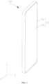
- FIG. 1 illustrates an electronic device 100 according to a first embodiment of the present disclosure.
- the electronic device 100 includes a display screen assembly 10.
- the electronic device 100 may be an electronic device having touch and display functions, such as a mobile phone, a notebook, a palmtop computer, an e-reader, a television, a smart home appliance, a smart operation screen, a smart home system, a wearable electronic device, a vehicle display, and the like.
- the present disclosure defines a length direction of the electronic device 100 as a direction Y, a width direction of the electronic device 100 as a direction X, and a thickness direction of the electronic device 100 as a direction Z.
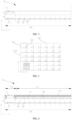
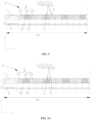
- FIG. 2 illustrates a display screen assembly 10 according to an embodiment of the present disclosure.
- the display screen assembly 10 includes a first display laminate 2 and a second display laminate 1 that are opposite to each other.
- a plurality of image sensors 21 is arranged on the first display laminate 2.
- a camera lens 11 is arranged on the second display laminate 1.
- the plurality of image sensors 21 directly faces the camera lens 11, and thus, the plurality of image sensors 21 can acquire image signals through the camera lens 11.
- an orthographic projection of the camera lens 11 on the first display laminate 2 may completely or partially cover the plurality of image sensors 21.
- the image sensors 21 and the camera lens 11 may form a camera module, i.e., a camera module configured to perform a photographing function.
- the components having the photographing function can be integrated in the display screen assembly 10 to reduce an area occupied by the camera module and increase an integration level of the components in the electronic device 100.
- installation processes of the camera module and a display screen in the related art may also be reduced, and it is unnecessary to reserve assembly space for the camera module in a middle frame, thereby saving space in the electronic device 100.
- the display screen assembly 10 may include a display portion 10a, and a non-display portion 10b surrounding the display portion 10a.
- the second display laminate 1 and the first display laminate 2 may form the display portion 10a.
- the camera lens 11 and the image sensors 21 can be integrated in the display portion 10a of the display screen assembly 10 to reduce an area in the non-display portion 10b of the display screen assembly 10 occupied by the camera module, thereby increasing a screen-to-body ratio of the electronic device 100.
- the first display laminate 2 may be a thin film transistor laminate.
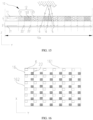
- the first display laminate 2 may include a plurality of scanning lines 161 (horizontal grid lines illustrated in FIG. 3 are all scanning lines), a plurality of data lines 162 (vertical grid lines illustrated in FIG. 3 are all data lines), and a plurality of thin film transistors 22.
- the plurality of scanning lines 161 intersects the plurality of data lines 162 to define a plurality of sub-pixel regions 16 arranged in an array. At least one of the thin film transistors 22 may be arranged in each sub-pixel region 16.
- the thin film transistor 22 may be electrically connected to the scanning line 161 and the data line 162. Referring to FIG.
- the plurality of image sensors 21 may be arranged outside the sub-pixel regions 16 and adjacent to the sub-pixel regions 16. In other embodiments, the plurality of image sensors 21 may be arranged in the sub-pixel regions 16.
- the data line 162 and the scanning line 161 may be electrically connected to the image sensor 21, and thus the data line 162 and the scanning line 161 may transmit signals to the image sensor 21 and the thin film transistor 22. In this way, the data line 162 and the scanning line 161 may be both used for dual purposes, a structure in the display screen assembly 10 may be simplified, and space of the display screen assembly 10 may be saved.
- a process of molding the image sensors 21 may be performed during a process of molding the thin film transistors 22; or the process of molding the image sensors 21 may overlap the process of molding the thin film transistors 22 to simplify processes of molding the image sensors 21 and the thin film transistors 22, thereby saving time and cost.
- the display screen assembly 10 may be a liquid crystal display screen or an organic light-emitting diode display screen.
- the first display laminate 2 may be a thin film transistor laminate
- the second display laminate 1 may be a color filter laminate.
- the first display laminate 2 may be a thin film transistor laminate
- the second display laminate 1 may be an encapsulation layer arranged on the thin film transistor laminate.
- the display screen assembly 10 is an organic light-emitting diode display screen.
- the second display laminate 1 may include a substrate 111, an organic light-emitting layer 112 arranged on the substrate 111, and an encapsulation layer 113 covering the organic light-emitting layer 112.
- the camera lens may be embedded in the encapsulation layer. 113.
- the encapsulation layer 113 has a covering portion 114 and an edge portion 115 surrounding the covering portion 114.
- the covering portion 114 covers the organic light-emitting layer 112.
- the edge portion 115 covers a peripheral region of the organic light-emitting layer 112.
- the camera lens 11 may be embedded in the edge portion 115.
- the edge portion 115 may cover the first display laminate 2. A distance between the edge portion 115 and the first display laminate 2 is small, and thus a distance between the camera lens 11 and the image sensors 21 is small, allowing the loss of light passing through the camera lens 11 to be small.
- the display screen assembly 10 is a liquid crystal display screen.
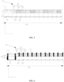
- the second display laminate 1 includes a plurality of color filters 12 adjacent to the camera lens 11.
- the plurality of color filters 12 and the plurality of sub-pixel regions 16 are arranged in one-to-one correspondence.
- the plurality of color filters 12 may include multiple red color resists 121, multiple green color resists 122, and multiple blue color resists 123.
- the plurality of color filters 12 may be arranged according to a certain pattern.
- the plurality of color filters 12 are arranged in a row and column array, which is present as an array of red, green and blue pixels.
- the plurality of color filters 12 may also present color of yellow, orange, etc.
- the plurality of color filters 12 may be the same or different sizes.
- an area occupied by the camera lens 11 may be an area occupied by the plurality of color filters 12, and this embodiment adopts such a structure as an example for description.
- a plurality of camera lenses 11 may be provided.
- An area occupied by each camera lens 11 may be an area of one color filter 12.
- the plurality of camera lenses 11 may be arranged in an array.
- the plurality of image sensors 21 may acquire image signals through the plurality of camera lenses 11 and compose image information frame by frame.
- the second display laminate 1 further includes a first light shielding block 13 and second light shielding blocks 14.
- the first light shielding block 13 surrounds the camera lens 11.
- the second light shielding blocks 14 is located between two adjacent color filters 12.
- the first light shielding block 13 and the second light shielding block 14 can be both configured to block visible light and prevent visible light from passing through.
- the first light shielding block 13 and the second light shielding block 14 may be black matrices in the display screen assembly 10.
- a material of the first light shielding block 13 and the second light shielding block 14 may be resin material or metal oxide that has good light shielding property.
- the first light shielding block 13 surrounds the camera lens 11 to prevent light emitted from the color filter 12 from interfering with image capture of the camera module. It can be understood that the first light shielding block 13 may define an annular cavity. The annular cavity is adapted to a shape of the camera lens 11. The camera lens 11 may be fixed in the annular cavity.
- the first light shielding block 13 is also configured to serve as a base for fixing the camera lens 11, allowing the camera lens 11 to be firmly assembled on the second display laminate 1. Meanwhile, an additional structure for fixing the camera lens 11 can be omitted, such that the first light shielding block 13 can be used for dual purposes.
- the second light shielding block 14 is located between two adjacent color filters 12 to prevent light crosstalk between different color filters 12 from causing image distortion.
- the thin film transistor 22 may directly face the second light shielding block 14, and thus the second light shielding block 14 can cover the thin film transistor 22.
- the first light shielding block 13 includes an extension portion 131 in a cylindrical shape.
- the extension portion 131 extends from the second display laminate 1 to the first display laminate 2.
- One end of the extension portion 131 surrounds a peripheral side of the camera lens 11, and the other end of the extension portion 131 surrounds a peripheral side of the plurality image sensors 21 on the first display laminate 2.
- the first light shielding block 13 may include a body 132, and the extension portion 131 connecting to the body 132.
- the body 132 of the first light shielding block 13 surrounds the camera lens 11.
- the extension portion 131 extends from an end of the body 132 close to the first display laminate 2 to the first display laminate 2.
- the extension portion 131 has a cylindrical shape.
- the extension portion 131 surrounds the plurality of image sensors 21. That is, the body 132 and the extension portion 131 are connected to each other to define an enclosing cavity in a cylindrical shape.
- the camera lens 11 is fixed at one end of the enclosing cavity.
- the plurality of image sensors 21 is located at the other end of the enclosing cavity.
- the enclosing cavity can prevent external light from interfering with the image sensors 21, thereby improving imaging quality of the image sensors 21.
- the extension portion 131 may be made of a light-shielding material and a material with certain rigidity, such that the extension portion 131 can have a shielding light function and a supporting function between the second display laminate 1 and the first display laminate 2.
- the extension portion 131 may be supported between the second display laminate 1 and the first display laminate 2 to define a spacing between the second display laminate 1 and the first display laminate 2.
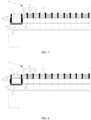
- the display screen assembly 10 may further include a backlight assembly 3.
- the backlight assembly 3 is located on a side of the first display laminate 2 facing away from the second display laminate 1.
- the backlight assembly 3 may be configured to emit visible light towards the first display laminate 2, such that the display portion 10a of the display screen assembly 10 can have display brightness.
- the backlight assembly 3 may be provided with a plurality of light-emitting sources 31.
- the plurality of light-emitting sources 31 may emit visible light towards the first display laminate 2.
- a light shielding sheet 15 may be provided on a side of the image sensors 21 close to the backlight assembly 3.
- the light shielding sheet 15 may be configured to shield the visible light emitted by the backlight assembly 3.
- the light shielding sheet 15 may be arranged on the first display laminate 2.
- the light shielding sheet 15 may be arranged between the image sensors 21 and the backlight assembly 3.
- the light shielding sheet 15 may be configured to shield the visible light emitted from the backlight assembly 3 towards the image sensors 21 and prevent the light from interfering with the image capture of the image sensors 21.
- the light-emitting source 31 on the backlight assembly 3 may be arranged at a position directly facing the thin film transistor 22, and the light-emitting source 31 may not be arranged in a region of the backlight assembly 3 directly facing the image sensor 21. In this way, light emitted by the light-emitting source 31 of the backlight assembly 3 may be directed towards the thin film transistor 22 and the color filter 12 to generate a display image.
- the light emitted by the light-emitting sources 31 of the backlight assembly 3 cannot be directed towards the image sensors 21, since the light is shielded by the light shielding sheet 15. Thus, the image sensors 21 can be protected from being interfered by the light emitted by the backlight assembly 3.
- an orthographic projection of the first light shielding block 13 on the first display laminate 2 may be located in the light shielding sheet 15.
- the light shielding sheet 15 may cover an opening of the extension portion 131 close to the first display laminate 2.
- the light shielding sheet 15 and the first light shielding block 13 may effectively shield light signals on a peripheral side of the image sensors 21 to prevent the image sensors 21 from being interfered by external light and to improve the imaging quality of the image sensor 21.
- the display screen assembly 10 may further include a light filter 4.
- the light filter 4 may be located between the camera lens 11 and the plurality of image sensors 21.
- the light filter 4 may be an infrared light filter 4.
- the light filter 4 may be configured to transmit visible light of a certain wavelength and reflect infrared light, for improving image capturing quality of the image sensors 21.
- the light filter 4 may also filter light of other wavelength bands to improve the imaging quality of the image sensors 21.
- the light filter 4 may be located on the second display laminate 1 and directly face the camera lens 11.
- the light filter 4 may directly face the camera lens 11 to remove interference light from light entering the camera lens 11. In this way, light received by the image sensor 21 does not include light interfering with image quality, thereby improving the imaging quality of the electronic device.
- the light filter 4 may be fixed in the enclosing cavity defined by the first light shielding block 13.
- the light filter 4 may also be arranged on a side of the second display laminate 1 facing away from the first display laminate 2 and directly face the camera lens 11; or the light filter 4 may also be arranged on the first display laminate 2 and directly face the multiple image sensors 21.
- FIG. 9 illustrates a display screen assembly in an electronic device 200 according to a second embodiment of the present disclosure.
- the second embodiment differs from the first embodiment in that, no light filter 4 is provided on the second display laminate 1. That is, interference light such as infrared light is not excluded from the light received by the image sensors 21.
- a chip configured to exclude the interference light may be arranged in the camera module. In this way, the interference light can be excluded from the image signal acquired by the image sensors 21 without providing the light filter 4.
- the display screen assembly 10 may further include a first emitter 5 and a receiver 6.
- the first emitter 5 may be located on the second display laminate 1.
- the first emitter 5 may be located on the first display laminate 2.
- the first emitter 5 may be located in a region outside the second display laminate 1 and the first display laminate 2.
- the first emitter 5 may be located between the second display laminate 1 and the first display laminate 2, on a side of the second display laminate 1 facing away from the first display laminate 2, on a side of the first display laminate 2 facing away from the second display laminate 1, in the non-display portion 10b of the display screen assembly 10, and the like.
- a position of the first emitter 5 is not limited, as long as an optical signal emitted by the first emitter 5 can be received by the receiver 6.
- the first emitter 5 may also be located on a structure in the electronic device other than the display screen assembly 10, for example, located on a housing of the electronic device, located in a gap between the housing and the display screen assembly 10 of the electronic device, and the like.
- an area of the non-display portion 10b of the display screen assembly 10 can be further reduced, and the screen-to-body ratio of the display screen assembly 10 can be further increased.
- the receiver 6 may be located on the first display laminate 2, and the receiver 6 may be connected to the thin film transistor 22.
- the receiver 6 may be configured to receive invisible light emitted by the first emitter 5.
- the invisible light may be any one of infrared light, ultraviolet light, or a combination of thereof.
- the receiver 6 and the first emitter 5 may be combined to form a proximity sensor configured to detect whether an approaching object is moving towards or away from the display screen, so as to perform operations such as awakening the display portion 10a of the display screen, turning off the screen brightness, or unlocking the screen.
- a plurality of receivers 6 and a plurality of transmitters 5 may be provided.
- the plurality of transmitters 5 and the plurality of receivers 6 can be combined to form a fingerprint recognition module or an iris recognition module.
- the invisible light emitted by the transmitter 5 may detect biometric information such as fingerprints, palm prints, joint prints, ear prints, iris, etc., so as to perform biometric recognition in the screen and to improve safety performance of the electronic device.
- the receiver 6 may also be configured as an ambient light sensor to detect brightness of an environment where the electronic device is located currently, and configured to adjust the display brightness of the display screen assembly 10 based on a detection result.
- the receiver 6 may include a photosensitive layer 61, and the photosensitive layer 61 has a special response.
- the photosensitive layer 61 may change its own resistance value based on an intensity of received invisible light, and a change in an intensity value of the invisible light can be obtained by detecting a change in the resistance value of the photosensitive layer 61.
- a material of the photosensitive layer 61 may be a semiconductor material such as lead sulfide.
- the thin film transistor 22 may include a gate layer 221, a gate insulating layer 222, a source and drain layer 223, a planarization layer 224 and a pixel electrode layer 225 that are stacked sequentially.
- the photosensitive layer 61 may be arranged on the same layer as the gate layer 221, or the source and drain layer 223, or the pixel electrode layer 225.
- a patterning of the photosensitive layer 61 may be performed during a molding process of patterning the gate layer 221, the source and drain layer 223, or the pixel electrode layer 225, thereby simplifying a molding process of the photosensitive layer 61 and saving time and manufacturing cost.
- the data line 162 and the scanning line 161 may also be electrically connected to the photosensitive layer 61 of the receiver 6 for data transmission between the photosensitive layer 61 and a chip of the receiver 6. That is, the receiver 6 may be connected to the thin film transistor 22 through the data line 162 and the scanning line 161. Consequently, the data line 162 and the scanning line 161 may serve as signal transmission lines for the thin film transistor 22, the image sensor 21, and the receiver 6. In this way, the data line 162 and the scanning line 161 both can be used for multiple purposes, thereby reducing the structures in the display screen assembly 10 and saving the space of the display screen assembly 10.
- a plurality of receivers 6 may be provided.
- the plurality of receivers 6 may directly face a region of the second display laminate 1 where the camera lens 11 is arranged.
- the camera lens 11 can converge invisible light to the plurality of receivers 6, so as to increase an intensity of the invisible light received by the receiver 6 and fully exert a light-converging function of the camera lens 11 at the same time.
- the plurality of image sensors 21 may be arranged in an array.
- the receiver 6 may be arranged between two adjacent image sensors 21. That is, the camera lens 11 directly faces a region where the plurality of image sensors 21 is located and a region where the plurality of receivers 6 is located. In this way, the image sensors 21 can acquire all image signals passing through the camera lens 11, and the receivers 6 can receive all invisible light signals passing through the camera lens 11, thereby improving the imaging quality of the image sensors 21 and increasing signal-receiving efficiency of the receiver 6 at the same time.
- the region where the plurality of image sensors 21 is located may be adjacent to the region where the plurality of receivers 6 is located.
- a plurality of receivers 6 may be provided. Each receiver 6 may be located on the first display laminate 2 in a region directly facing the color filter 12. Each receiver 6 may be located between two adjacent thin film transistors 22.
- a plurality of receivers 6 may be provided.
- One or more receivers 6 may be located in one sub-pixel region 16.
- one thin film transistor 22 and at least one receiver 6 are provided in each sub-pixel region 16.
- the receiver 6 and the thin film transistor 22 located in the same sub-pixel region 16 may be adjacent to each other or in diagonal, so as to reduce mutual interference between the receiver 6 and the thin film transistor 22 and to increase an aperture ratio of the sub-pixel region 16.
- the receiver 6 may also be located outside the sub-pixel region 16, for example, located between two adjacent sub-pixel regions 16.
- the display screen assembly 10 may further include a backlight assembly 3.
- the backlight assembly 3 may face the side of the first display laminate 2 facing away from the second display laminate 1.
- the backlight assembly 3 may be configured to emit visible light towards the first display laminate 2.
- the first emitter 5 may be located on the backlight assembly 3.
- the first emitter 5 may be configured to emit invisible light towards the first display laminate 2.
- the first emitter 5 may be a light-emitting diode (LED) lamp, a mini-LED lamp, or a micro-LED lamp.
- the first emitter 5 may be arranged on the backlight assembly 3.
- the first emitter 5 and the light-emitting sources 31 on the backlight assembly 3 may share a driving circuit and a controller, without additionally providing a driving circuit and a controller for the first emitter 5. In this way, the space on the backlight assembly 3 can be saved, and a utilization rate of the original structure can be improved.
- the backlight assembly 3 may have a first backlight portion 32 and a second backlight portion 33 that are connected to each other.
- the first backlight portion 32 may directly face the region where the plurality of image sensors 21 is located.
- the second backlight portion 33 may directly face the region where the plurality thin film transistors 22 is located.
- a plurality of first emitters 5 is provided. The first emitters 5 may be located in the first backlight portion 32.
- the first emitters 5 may directly face the plurality of image sensors 21.
- the invisible light emitted by the first emitters 5 may be emitted through the plurality of image sensors 21 and the camera lens 11, and then reflected and projected onto the receivers 6 arranged on the first display laminate 2.
- the receiver 6 may be arranged on the first display laminate 2 in a region where the thin film transistor 22 are arranged, and the receiver 6 may be configured to capture fingerprint or detect distance. In other embodiments, the receiver 6 may also be located on the first display laminate 2 in a region where the image sensors 21 are arranged.
- the backlight assembly 3 may further include a plurality of second emitters 34.
- the plurality of second emitters 34 is configured to emit visible light towards the second display laminate 1.
- the plurality of second emitters 34 may be located in the second backlight portion 33. Since the visible light sources of the backlight assembly 3 directly face the thin film transistors 22 and offset from a region where the image sensors 21 and the camera lens are located, the interference of the visible light sources on image signal acquisition of the image sensor 21 may be reduced. Meanwhile, the first emitter 5 emitting invisible light is provided in a region of the backlight assembly 3 directly facing the image sensors 21 to utilize the space on the backlight assembly 3 reasonably. In addition, the invisible light emitted by the first emitter 5 does not interfere with image information acquired by the image sensor 21, thereby improving the quality of image capture.
- the backlight assembly 3 may have a first backlight portion 32 and a second backlight portion 33 that are connected to each other.
- the first backlight portion 32 may directly face the region where the plurality of image sensors 21 is located.
- the second backlight portion 33 may directly face the region where the plurality of thin film transistors 22 is located.
- the first emitter 5 may be located at a position on the second backlight portion 33 close to the first backlight portion 32. That is, the first emitter 5 may be located on the backlight assembly 3 in the region directly facing the thin film transistors 22.
- the receiver 6 may be located on the first display laminate 2 in the region where the plurality of image sensors 21 is arranged or located on the first display laminate 2 in the region where the thin film transistors 22 are arranged. Alternatively, the receiver 6 may also be located on the backlight assembly 3 in the region directly facing the plurality of image sensors 21.
- the backlight assembly 3 may further include a plurality of second emitters 34 arranged in an array.
- the plurality of second emitters 34 may be configured to emit the visible light towards the second display laminate 1.
- the plurality of second emitters 34 may be located on the second backlight portion 33.
- a plurality of first emitters 5 is provided.
- the first emitter 5 may be arranged between two adjacent second emitters 34. That is, the first emitters 5 and the second emitters 34 are located in a region directly facing the thin film transistors 22.
- the first emitter 5 may be located between two adjacent second emitters 34.
- the plurality of first emitters 5 may be distributed over the entire second backlight portion 33, that is, the entire display portion 10a of the display screen assembly 10 can perform fingerprint detection, or proximity detection, or ambient light detection, and the like.
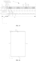
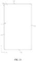
- the second display laminate 1 may include two opposite long sides 171, 172 and two opposite short sides 173, 174.
- the two long sides 171, 172 may be connected between the two short sides 173, 174.
- the camera lens 11 is close to one short side 173; or referring to FIG. 21 , the camera lens 11 is close to one long side 171; or referring to FIG. 22 , the camera lens 11 is close to a position where one long side 171 and one short side 173 are connected to each other.
- a region for a photographing function and a region for a display function of the electronic device can be separated, and thus the photographing function and the display function will not interfere with each other, thereby improving user experience of the electronic device.
Landscapes
- Engineering & Computer Science (AREA)
- Signal Processing (AREA)
- Multimedia (AREA)
- Theoretical Computer Science (AREA)
- Human Computer Interaction (AREA)
- Physics & Mathematics (AREA)
- Computer Hardware Design (AREA)
- General Engineering & Computer Science (AREA)
- General Physics & Mathematics (AREA)
- Microelectronics & Electronic Packaging (AREA)
- Optics & Photonics (AREA)
- Geometry (AREA)
- Devices For Indicating Variable Information By Combining Individual Elements (AREA)
Claims (12)
- Anzeigebildschirmanordnung (10), umfassend:ein erstes Anzeigelaminat (2) und ein zweites Anzeigelaminat (1), die einander gegenüberliegen;eine Vielzahl von Bildsensoren (21), angeordnet auf dem ersten Anzeigelaminat (2); undein Kameraobjektiv (11), angeordnet auf dem zweiten Anzeigelaminat (1),wobei die Vielzahl von Bildsensoren (21) direkt dem Kameraobjektiv (11) zugewandt ist und die Vielzahl von Bildsensoren (21) dazu konfiguriert ist, Bildsignale durch das Kameraobjektiv (11) zu erfassen,dadurch gekennzeichnet, dassdas zweite Anzeigelaminat (1) eine Vielzahl von Farbfiltern (12) neben dem Kameraobjektiv (11), einen ersten Lichtabschirmungsblock (13) und eine Vielzahl zweiter Lichtabschirmungsblöcke (14) umfasst, die voneinander beabstandet sind; die Vielzahl von Farbfiltern (12) einer Vielzahl von Subpixelbereichen (16) in einer Eins-zu-eins-Entsprechung entspricht; jeder der Vielzahl zweiter Lichtabschirmungsblöcke (14) sich zwischen zwei benachbarten Farbfiltern (12) der Vielzahl von Farbfiltern (12) befindet und der erste Lichtabschirmungsblock (13) und die Vielzahl zweiter Lichtabschirmungsblöcke (14) dazu konfiguriert sind, sichtbares Licht abzuschirmen,der erste Lichtabschirmungsblock (13) einen Erweiterungsabschnitt (131) in zylindrischer Form umfasst, wobei sich der Erweiterungsabschnitt (131) von dem zweiten Anzeigelaminat (1) zu dem ersten Anzeigelaminat (2) erstreckt, ein Ende des Erweiterungsabschnitts (131) die Umfangsseite des Kameraobjektivs (11) umgibt und das andere Ende des Erweiterungsabschnitts (131) eine Umfangsseite der Vielzahl von Bildsensoren (21) umgibt.
- Anzeigebildschirmanordnung (10) nach Anspruch 1, wobei das erste Anzeigelaminat (2) eine Vielzahl von Abtastleitungen (161), eine Vielzahl von Datenleitungen (162) und eine Vielzahl von Dünnschichttransistoren (22) umfasst;die Vielzahl von Abtastleitungen (161) die Vielzahl von Datenleitungen (162) schneidet, um die Vielzahl von in einem Array angeordneten Subpixelbereiche (16) zu definieren;mindestens einer der Vielzahl von Dünnschichttransistoren (22) in einem der Vielzahl von Subpixelbereichen (16) angeordnet ist; unddie Vielzahl von Bildsensoren (21) sich außerhalb der Vielzahl von Subpixelbereichen (16) und benachbart zu der Vielzahl von Subpixelbereichen (16) befindet oder die Vielzahl von Bildsensoren (21) in der Vielzahl von Subpixelbereichen (16) angeordnet ist.
- Anzeigebildschirmanordnung (10) nach Anspruch 1, wobei das zweite Anzeigelaminat (1) ferner ein Substrat (111), eine auf dem Substrat (111) angeordnete organische lichtemittierende Schicht (112) und eine Einkapselungsschicht (113), die die organische lichtemittierende Schicht (112) bedeckt, umfasst, wobei das Kameraobjektiv (11) in der Einkapselungsschicht (113) eingebettet ist.
- Anzeigebildschirmanordnung (10) nach Anspruch 3, wobei die Einkapselungsschicht (113) einen Abdeckabschnitt (114) und einen Randabschnitt (115) umfasst, der den Abdeckabschnitt (114) umgibt, wobei der Abdeckabschnitt (114) dazu konfiguriert ist, die organische lichtemittierende Schicht (112) abzudecken, der Randabschnitt (115) dazu konfiguriert ist, einen Randbereich der organischen lichtemittierenden Schicht (112) abzudecken, und das Kameraobjektiv (11) in dem Randabschnitt (115) eingebettet ist.
- Anzeigebildschirmanordnung (10) nach einem der Ansprüche 1 bis 4, ferner umfassend einen ersten Emitter (5) und einen Empfänger (6),wobei sich der Empfänger (6) auf dem ersten Anzeigelaminat (2) befindet und der Empfänger (6) dazu konfiguriert ist, unsichtbares Licht zu empfangen, das von dem ersten Emitter (5) emittiert und von einem zu erkennenden Objekt reflektiert wird, oder der Empfänger (6) dazu konfiguriert ist, die Helligkeit des Umgebungslichts zu erkennen, undwobei der erste Emitter (5) sich auf dem zweiten Anzeigelaminat (1) befindet; oder der erste Emitter (5) sich auf dem ersten Anzeigelaminat (2) befindet; oder der erste Emitter (5) sich in einem Bereich außerhalb des zweiten Anzeigelaminats (1) und des ersten Anzeigelaminats (2) befindet.
- Anzeigebildschirmanordnung (10) nach Anspruch 5, wobei eine Vielzahl von Empfängern (6) bereitgestellt ist und die Vielzahl von Empfängern (6) direkt einem Bereich des zweiten Anzeigelaminats (1) zugewandt ist, in dem das Kameraobjektiv (11) angeordnet ist, und
wobei die Vielzahl von Bildsensoren (21) in einem Array angeordnet ist und jeder der Vielzahl von Empfängern (6) zwischen zwei benachbarten Bildsensoren (21) der Vielzahl von Bildsensoren (21) angeordnet ist. - Anzeigebildschirmanordnung (10) nach Anspruch 5, wobei eine Vielzahl von Empfängern (6) bereitgestellt ist, wobei einer oder mehrere Empfänger der Vielzahl von Empfängern (6) sich in einem Subpixelbereich der Vielzahl von Subpixelbereichen (16) befinden und der eine oder die mehreren Empfänger (6) und der mindestens eine der Vielzahl von Dünnschichttransistoren (22), die sich in dem einen Subpixelbereich (16) befinden, benachbart zueinander oder in einer Diagonale angeordnet sind.
- Anzeigebildschirmanordnung (10) nach Anspruch 7, ferner umfassend eine Hintergrundbeleuchtungsanordnung (3), wobei die Hintergrundbeleuchtungsanordnung (3) einer Seite des ersten Anzeigelaminats (2) zugewandt ist, die dem zweiten Anzeigelaminat (1) abgewandt ist, wobei der erste Emitter (5) sich auf der Hintergrundbeleuchtungsanordnung (3) befindet und der erste Emitter (5) dazu konfiguriert ist, das unsichtbare Licht in Richtung des ersten Anzeigelaminats (2) zu emittieren.
- Anzeigebildschirmanordnung (10) nach Anspruch 8, wobei die Hintergrundbeleuchtungsanordnung (3) einen ersten Hintergrundbeleuchtungsabschnitt (32) und einen zweiten Hintergrundbeleuchtungsabschnitt (33) umfasst, die direkt miteinander verbunden sind, wobei der erste Hintergrundbeleuchtungsabschnitt (32) direkt einem Bereich zugewandt ist, in dem sich die Vielzahl von Bildsensoren (21) befindet, der zweite Hintergrundbeleuchtungsabschnitt (33) direkt einem Bereich zugewandt ist, in dem sich die Vielzahl von Dünnschichttransistoren (22) befindet, eine Vielzahl erster Emitter (5) bereitgestellt ist, und die Vielzahl erster Emitter (5) sich in dem ersten Hintergrundbeleuchtungsabschnitt (32) befindet.
- Anzeigebildschirmanordnung (10) nach Anspruch 8, wobei die Hintergrundbeleuchtungsanordnung (3) einen ersten Hintergrundbeleuchtungsabschnitt (32) und einen zweiten Hintergrundbeleuchtungsabschnitt (33) umfasst, die direkt miteinander verbunden sind, wobei der erste Hintergrundbeleuchtungsabschnitt (32) direkt einem Bereich zugewandt ist, in dem sich die Vielzahl von Bildsensoren (21) befindet, der zweite Hintergrundbeleuchtungsabschnitt (33) direkt einem Bereich zugewandt ist, in dem sich die Vielzahl von Dünnschichttransistoren (22) befindet, und der erste Emitter (5) sich an einer Position des zweiten Hintergrundbeleuchtungsabschnitts (33) in der Nähe des ersten Hintergrundbeleuchtungsabschnitts (32) befindet.
- Anzeigebildschirmanordnung (10) nach Anspruch 10, wobei die Hintergrundbeleuchtungsanordnung (3) ferner eine Vielzahl zweiter Emitter (34) umfasst, angeordnet in einem Array, wobei die Vielzahl zweiter Emitter (34) dazu konfiguriert ist, sichtbares Licht in Richtung des zweiten Anzeigelaminats (1) zu emittieren, die Vielzahl zweiter Emitter (34) auf dem zweiten Hintergrundbeleuchtungsabschnitt (33) befindet eine Vielzahl erster Emitter (5) bereitgestellt ist, wobei jeder der Vielzahl erster Emitter (5) angeordnet ist zwischen zwei benachbarten zweiten Emittern der Vielzahl zweiter Emitter (34).
- Elektronische Vorrichtung (100), umfassend die Anzeigebildschirmanordnung (10) nach einem der Ansprüche 1 bis 10.
Applications Claiming Priority (2)
| Application Number | Priority Date | Filing Date | Title |
|---|---|---|---|
| CN201811444936.8A CN109688308B (zh) | 2018-11-29 | 2018-11-29 | 显示屏组件及电子设备 |
| PCT/CN2019/112584 WO2020108174A1 (zh) | 2018-11-29 | 2019-10-22 | 显示屏组件及电子设备 |
Publications (3)
| Publication Number | Publication Date |
|---|---|
| EP3883233A1 EP3883233A1 (de) | 2021-09-22 |
| EP3883233A4 EP3883233A4 (de) | 2022-01-12 |
| EP3883233B1 true EP3883233B1 (de) | 2023-08-09 |
Family
ID=66184994
Family Applications (1)
| Application Number | Title | Priority Date | Filing Date |
|---|---|---|---|
| EP19890587.9A Active EP3883233B1 (de) | 2018-11-29 | 2019-10-22 | Anzeigebildschirmanordnung und elektronische vorrichtung |
Country Status (4)
| Country | Link |
|---|---|
| US (1) | US20210258411A1 (de) |
| EP (1) | EP3883233B1 (de) |
| CN (1) | CN109688308B (de) |
| WO (1) | WO2020108174A1 (de) |
Families Citing this family (11)
| Publication number | Priority date | Publication date | Assignee | Title |
|---|---|---|---|---|
| CN109688308B (zh) * | 2018-11-29 | 2021-03-09 | Oppo广东移动通信有限公司 | 显示屏组件及电子设备 |
| CN112019766B (zh) * | 2019-05-31 | 2022-03-18 | 比亚迪股份有限公司 | 中央控制台和车辆 |
| CN110278332A (zh) * | 2019-06-30 | 2019-09-24 | Oppo广东移动通信有限公司 | 电子设备及电子设备的控制方法 |
| CN110488524A (zh) * | 2019-08-13 | 2019-11-22 | 武汉华星光电技术有限公司 | 显示装置、显示装置中摄像的方法 |
| CN110703485B (zh) * | 2019-09-18 | 2021-11-16 | 昆山龙腾光电股份有限公司 | 一种液晶显示面板及其制作方法 |
| CN112684644B (zh) * | 2019-10-18 | 2025-06-24 | 北京小米移动软件有限公司 | 显示面板和电子设备 |
| CN112684638B (zh) | 2019-10-18 | 2022-10-11 | 北京小米移动软件有限公司 | 显示面板和电子设备 |
| CN111818264B (zh) * | 2020-07-15 | 2021-10-19 | Oppo广东移动通信有限公司 | 图像采集系统 |
| CN116635769A (zh) * | 2021-01-18 | 2023-08-22 | 三星电子株式会社 | 包括微型相机的可穿戴的电子装置 |
| CN113093422B (zh) * | 2021-03-23 | 2022-12-23 | 深圳市华星光电半导体显示技术有限公司 | 显示面板及显示面板的制备方法 |
| CN115225740B (zh) * | 2022-06-06 | 2023-07-14 | 荣耀终端有限公司 | 一种电子设备、显示屏及成像方法 |
Family Cites Families (24)
| Publication number | Priority date | Publication date | Assignee | Title |
|---|---|---|---|---|
| US20080225216A1 (en) * | 2007-03-15 | 2008-09-18 | Seiko Epson Corporation | Active matrix circuit substrate and display device |
| TW201123869A (en) * | 2009-12-25 | 2011-07-01 | Hon Hai Prec Ind Co Ltd | Camera module and method of manufacturing same |
| JP4999979B2 (ja) * | 2010-12-09 | 2012-08-15 | 株式会社半導体エネルギー研究所 | イメージセンサ及び電子機器 |
| US20140218587A1 (en) * | 2013-02-07 | 2014-08-07 | Motorola Mobility Llc | Double sided camera module |
| CN104793390A (zh) * | 2015-01-31 | 2015-07-22 | 业鑫科技顾问股份有限公司 | 显示面板、薄膜晶体管基板、彩色滤光片基板及制作方法 |
| CN104795418B (zh) * | 2015-04-24 | 2018-09-18 | 上海珏芯光电科技有限公司 | 感光成像装置及其制造方法 |
| CN204808361U (zh) * | 2015-07-29 | 2015-11-25 | 京东方科技集团股份有限公司 | 一种基板、指纹识别传感器、指纹识别装置 |
| US20160005362A1 (en) * | 2015-09-08 | 2016-01-07 | Mediatek Inc. | Determination Of Optical Condition And Adjustment Of Display |
| KR102490891B1 (ko) * | 2015-12-04 | 2023-01-25 | 삼성디스플레이 주식회사 | 표시 장치 |
| CN105718105B (zh) * | 2015-12-25 | 2018-12-11 | 业成科技(成都)有限公司 | 有机发光二极管触控显示面板 |
| CN106056099A (zh) * | 2016-06-23 | 2016-10-26 | 京东方科技集团股份有限公司 | 一种指纹识别显示面板及显示装置 |
| CN206524899U (zh) * | 2017-01-22 | 2017-09-26 | 瑞声科技(新加坡)有限公司 | 视觉传感器模组 |
| CN106935144B (zh) * | 2017-04-17 | 2019-07-23 | Oppo广东移动通信有限公司 | 显示模组和终端设备 |
| CN107167945B (zh) * | 2017-04-24 | 2021-01-12 | Oppo广东移动通信有限公司 | 显示装置与移动电子终端 |
| CN107229148B (zh) * | 2017-05-05 | 2021-03-09 | Oppo广东移动通信有限公司 | 显示屏、显示装置及移动终端 |
| CN107393458B (zh) * | 2017-07-28 | 2019-11-15 | 武汉华星光电半导体显示技术有限公司 | 一种柔性显示面板及装置 |
| CN107707695A (zh) * | 2017-09-29 | 2018-02-16 | 努比亚技术有限公司 | 全面屏、终端设备及其制作方法 |
| CN107592444B (zh) * | 2017-10-30 | 2019-10-25 | 北京京东方显示技术有限公司 | 一种显示面板和显示装置 |
| KR102419066B1 (ko) * | 2017-11-20 | 2022-07-08 | 엘지디스플레이 주식회사 | 터치 디스플레이 패널 및 터치 디스플레이 장치 |
| CN108196388B (zh) * | 2018-02-12 | 2022-04-19 | 京东方科技集团股份有限公司 | 一种显示装置及其制造方法 |
| CN108566460B (zh) * | 2018-04-18 | 2020-01-31 | Oppo广东移动通信有限公司 | 显示屏组件及电子设备 |
| CN108881526B (zh) * | 2018-05-23 | 2024-11-19 | Oppo广东移动通信有限公司 | 电子装置 |
| CN108761885A (zh) * | 2018-08-13 | 2018-11-06 | 京东方科技集团股份有限公司 | 阵列基板及其制作方法、彩膜基板、显示面板和显示装置 |
| CN109688308B (zh) * | 2018-11-29 | 2021-03-09 | Oppo广东移动通信有限公司 | 显示屏组件及电子设备 |
-
2018
- 2018-11-29 CN CN201811444936.8A patent/CN109688308B/zh active Active
-
2019
- 2019-10-22 WO PCT/CN2019/112584 patent/WO2020108174A1/zh not_active Ceased
- 2019-10-22 EP EP19890587.9A patent/EP3883233B1/de active Active
-
2021
- 2021-05-06 US US17/313,378 patent/US20210258411A1/en not_active Abandoned
Also Published As
| Publication number | Publication date |
|---|---|
| CN109688308B (zh) | 2021-03-09 |
| US20210258411A1 (en) | 2021-08-19 |
| EP3883233A1 (de) | 2021-09-22 |
| WO2020108174A1 (zh) | 2020-06-04 |
| CN109688308A (zh) | 2019-04-26 |
Similar Documents
| Publication | Publication Date | Title |
|---|---|---|
| EP3883233B1 (de) | Anzeigebildschirmanordnung und elektronische vorrichtung | |
| EP3605207B1 (de) | Array-substrat, anzeigebildschirm und elektronische vorrichtung | |
| KR102666192B1 (ko) | 표시 장치 | |
| US11361583B2 (en) | Fingerprint identification apparatus and electronic device | |
| CN109859648B (zh) | 一种显示面板及显示装置 | |
| CN114141837B (zh) | 一种oled显示模组及显示终端 | |
| CN108388056B (zh) | 显示面板及其制作方法 | |
| US10627937B2 (en) | Display module | |
| EP3919971B1 (de) | Anzeigeanordnung und deren herstellungsverfahren, elektronische vorrichtung | |
| US20210366996A1 (en) | Display panel and electronic device | |
| CN111384084A (zh) | 显示面板和智能终端 | |
| CN110515226A (zh) | 电子设备、显示组件及其显示面板 | |
| WO2021051710A1 (zh) | 指纹感测模块与电子装置 | |
| CN111405084A (zh) | 显示面板和智能终端 | |
| US11594818B2 (en) | Electronic apparatus | |
| CN110098180B (zh) | 晶圆级感应模块及其制造方法 | |
| CN110865727B (zh) | 电子装置 | |
| CN214799620U (zh) | 电子设备 | |
| CN224067206U (zh) | 电子装置 | |
| US20250351710A1 (en) | Display device | |
| CN111915996B (zh) | 微型发光二极管显示器 | |
| RU2780043C2 (ru) | Узел экрана дисплея и электронное устройство | |
| CN115022425A (zh) | 图像传感模组及电子设备 | |
| CN117135955A (zh) | 电子装置 | |
| HK1263090A1 (en) | Array substrate, display screen and electronic device |
Legal Events
| Date | Code | Title | Description |
|---|---|---|---|
| STAA | Information on the status of an ep patent application or granted ep patent |
Free format text: STATUS: THE INTERNATIONAL PUBLICATION HAS BEEN MADE |
|
| PUAI | Public reference made under article 153(3) epc to a published international application that has entered the european phase |
Free format text: ORIGINAL CODE: 0009012 |
|
| STAA | Information on the status of an ep patent application or granted ep patent |
Free format text: STATUS: REQUEST FOR EXAMINATION WAS MADE |
|
| 17P | Request for examination filed |
Effective date: 20210614 |
|
| AK | Designated contracting states |
Kind code of ref document: A1 Designated state(s): AL AT BE BG CH CY CZ DE DK EE ES FI FR GB GR HR HU IE IS IT LI LT LU LV MC MK MT NL NO PL PT RO RS SE SI SK SM TR |
|
| A4 | Supplementary search report drawn up and despatched |
Effective date: 20211209 |
|
| RIC1 | Information provided on ipc code assigned before grant |
Ipc: H01L 27/32 20060101ALI20211203BHEP Ipc: H04M 1/02 20060101ALI20211203BHEP Ipc: H04N 5/225 20060101AFI20211203BHEP |
|
| DAV | Request for validation of the european patent (deleted) | ||
| DAX | Request for extension of the european patent (deleted) | ||
| REG | Reference to a national code |
Ref country code: DE Ref legal event code: R079 Free format text: PREVIOUS MAIN CLASS: H04N0005225000 Ref country code: DE Ref legal event code: R079 Ref document number: 602019034870 Country of ref document: DE Free format text: PREVIOUS MAIN CLASS: H04N0005225000 Ipc: G06F0001160000 |
|
| GRAP | Despatch of communication of intention to grant a patent |
Free format text: ORIGINAL CODE: EPIDOSNIGR1 |
|
| RIC1 | Information provided on ipc code assigned before grant |
Ipc: H04M 1/02 20060101ALI20230330BHEP Ipc: H04N 23/57 20230101ALI20230330BHEP Ipc: H04N 23/55 20230101ALI20230330BHEP Ipc: H04N 23/54 20230101ALI20230330BHEP Ipc: H04N 23/45 20230101ALI20230330BHEP Ipc: G06F 1/16 20060101AFI20230330BHEP |
|
| STAA | Information on the status of an ep patent application or granted ep patent |
Free format text: STATUS: GRANT OF PATENT IS INTENDED |
|
| INTG | Intention to grant announced |
Effective date: 20230504 |
|
| GRAS | Grant fee paid |
Free format text: ORIGINAL CODE: EPIDOSNIGR3 |
|
| GRAA | (expected) grant |
Free format text: ORIGINAL CODE: 0009210 |
|
| STAA | Information on the status of an ep patent application or granted ep patent |
Free format text: STATUS: THE PATENT HAS BEEN GRANTED |
|
| AK | Designated contracting states |
Kind code of ref document: B1 Designated state(s): AL AT BE BG CH CY CZ DE DK EE ES FI FR GB GR HR HU IE IS IT LI LT LU LV MC MK MT NL NO PL PT RO RS SE SI SK SM TR |
|
| REG | Reference to a national code |
Ref country code: GB Ref legal event code: FG4D |
|
| REG | Reference to a national code |
Ref country code: CH Ref legal event code: EP |
|
| REG | Reference to a national code |
Ref country code: DE Ref legal event code: R096 Ref document number: 602019034870 Country of ref document: DE |
|
| REG | Reference to a national code |
Ref country code: IE Ref legal event code: FG4D |
|
| P01 | Opt-out of the competence of the unified patent court (upc) registered |
Effective date: 20231016 |
|
| REG | Reference to a national code |
Ref country code: LT Ref legal event code: MG9D |
|
| REG | Reference to a national code |
Ref country code: NL Ref legal event code: MP Effective date: 20230809 |
|
| REG | Reference to a national code |
Ref country code: AT Ref legal event code: MK05 Ref document number: 1598267 Country of ref document: AT Kind code of ref document: T Effective date: 20230809 |
|
| PG25 | Lapsed in a contracting state [announced via postgrant information from national office to epo] |
Ref country code: GR Free format text: LAPSE BECAUSE OF FAILURE TO SUBMIT A TRANSLATION OF THE DESCRIPTION OR TO PAY THE FEE WITHIN THE PRESCRIBED TIME-LIMIT Effective date: 20231110 |
|
| PGFP | Annual fee paid to national office [announced via postgrant information from national office to epo] |
Ref country code: GB Payment date: 20231024 Year of fee payment: 5 |
|
| PG25 | Lapsed in a contracting state [announced via postgrant information from national office to epo] |
Ref country code: IS Free format text: LAPSE BECAUSE OF FAILURE TO SUBMIT A TRANSLATION OF THE DESCRIPTION OR TO PAY THE FEE WITHIN THE PRESCRIBED TIME-LIMIT Effective date: 20231209 |
|
| PG25 | Lapsed in a contracting state [announced via postgrant information from national office to epo] |
Ref country code: SE Free format text: LAPSE BECAUSE OF FAILURE TO SUBMIT A TRANSLATION OF THE DESCRIPTION OR TO PAY THE FEE WITHIN THE PRESCRIBED TIME-LIMIT Effective date: 20230809 Ref country code: RS Free format text: LAPSE BECAUSE OF FAILURE TO SUBMIT A TRANSLATION OF THE DESCRIPTION OR TO PAY THE FEE WITHIN THE PRESCRIBED TIME-LIMIT Effective date: 20230809 Ref country code: PT Free format text: LAPSE BECAUSE OF FAILURE TO SUBMIT A TRANSLATION OF THE DESCRIPTION OR TO PAY THE FEE WITHIN THE PRESCRIBED TIME-LIMIT Effective date: 20231211 Ref country code: NO Free format text: LAPSE BECAUSE OF FAILURE TO SUBMIT A TRANSLATION OF THE DESCRIPTION OR TO PAY THE FEE WITHIN THE PRESCRIBED TIME-LIMIT Effective date: 20231109 Ref country code: NL Free format text: LAPSE BECAUSE OF FAILURE TO SUBMIT A TRANSLATION OF THE DESCRIPTION OR TO PAY THE FEE WITHIN THE PRESCRIBED TIME-LIMIT Effective date: 20230809 Ref country code: LV Free format text: LAPSE BECAUSE OF FAILURE TO SUBMIT A TRANSLATION OF THE DESCRIPTION OR TO PAY THE FEE WITHIN THE PRESCRIBED TIME-LIMIT Effective date: 20230809 Ref country code: LT Free format text: LAPSE BECAUSE OF FAILURE TO SUBMIT A TRANSLATION OF THE DESCRIPTION OR TO PAY THE FEE WITHIN THE PRESCRIBED TIME-LIMIT Effective date: 20230809 Ref country code: IS Free format text: LAPSE BECAUSE OF FAILURE TO SUBMIT A TRANSLATION OF THE DESCRIPTION OR TO PAY THE FEE WITHIN THE PRESCRIBED TIME-LIMIT Effective date: 20231209 Ref country code: HR Free format text: LAPSE BECAUSE OF FAILURE TO SUBMIT A TRANSLATION OF THE DESCRIPTION OR TO PAY THE FEE WITHIN THE PRESCRIBED TIME-LIMIT Effective date: 20230809 Ref country code: GR Free format text: LAPSE BECAUSE OF FAILURE TO SUBMIT A TRANSLATION OF THE DESCRIPTION OR TO PAY THE FEE WITHIN THE PRESCRIBED TIME-LIMIT Effective date: 20231110 Ref country code: FI Free format text: LAPSE BECAUSE OF FAILURE TO SUBMIT A TRANSLATION OF THE DESCRIPTION OR TO PAY THE FEE WITHIN THE PRESCRIBED TIME-LIMIT Effective date: 20230809 Ref country code: AT Free format text: LAPSE BECAUSE OF FAILURE TO SUBMIT A TRANSLATION OF THE DESCRIPTION OR TO PAY THE FEE WITHIN THE PRESCRIBED TIME-LIMIT Effective date: 20230809 |
|
| PGFP | Annual fee paid to national office [announced via postgrant information from national office to epo] |
Ref country code: FR Payment date: 20231020 Year of fee payment: 5 Ref country code: DE Payment date: 20231023 Year of fee payment: 5 |
|
| PG25 | Lapsed in a contracting state [announced via postgrant information from national office to epo] |
Ref country code: PL Free format text: LAPSE BECAUSE OF FAILURE TO SUBMIT A TRANSLATION OF THE DESCRIPTION OR TO PAY THE FEE WITHIN THE PRESCRIBED TIME-LIMIT Effective date: 20230809 |
|
| PG25 | Lapsed in a contracting state [announced via postgrant information from national office to epo] |
Ref country code: ES Free format text: LAPSE BECAUSE OF FAILURE TO SUBMIT A TRANSLATION OF THE DESCRIPTION OR TO PAY THE FEE WITHIN THE PRESCRIBED TIME-LIMIT Effective date: 20230809 |
|
| PG25 | Lapsed in a contracting state [announced via postgrant information from national office to epo] |
Ref country code: SM Free format text: LAPSE BECAUSE OF FAILURE TO SUBMIT A TRANSLATION OF THE DESCRIPTION OR TO PAY THE FEE WITHIN THE PRESCRIBED TIME-LIMIT Effective date: 20230809 Ref country code: RO Free format text: LAPSE BECAUSE OF FAILURE TO SUBMIT A TRANSLATION OF THE DESCRIPTION OR TO PAY THE FEE WITHIN THE PRESCRIBED TIME-LIMIT Effective date: 20230809 Ref country code: ES Free format text: LAPSE BECAUSE OF FAILURE TO SUBMIT A TRANSLATION OF THE DESCRIPTION OR TO PAY THE FEE WITHIN THE PRESCRIBED TIME-LIMIT Effective date: 20230809 Ref country code: EE Free format text: LAPSE BECAUSE OF FAILURE TO SUBMIT A TRANSLATION OF THE DESCRIPTION OR TO PAY THE FEE WITHIN THE PRESCRIBED TIME-LIMIT Effective date: 20230809 Ref country code: DK Free format text: LAPSE BECAUSE OF FAILURE TO SUBMIT A TRANSLATION OF THE DESCRIPTION OR TO PAY THE FEE WITHIN THE PRESCRIBED TIME-LIMIT Effective date: 20230809 Ref country code: CZ Free format text: LAPSE BECAUSE OF FAILURE TO SUBMIT A TRANSLATION OF THE DESCRIPTION OR TO PAY THE FEE WITHIN THE PRESCRIBED TIME-LIMIT Effective date: 20230809 Ref country code: SK Free format text: LAPSE BECAUSE OF FAILURE TO SUBMIT A TRANSLATION OF THE DESCRIPTION OR TO PAY THE FEE WITHIN THE PRESCRIBED TIME-LIMIT Effective date: 20230809 |
|
| REG | Reference to a national code |
Ref country code: DE Ref legal event code: R097 Ref document number: 602019034870 Country of ref document: DE |
|
| PG25 | Lapsed in a contracting state [announced via postgrant information from national office to epo] |
Ref country code: IT Free format text: LAPSE BECAUSE OF FAILURE TO SUBMIT A TRANSLATION OF THE DESCRIPTION OR TO PAY THE FEE WITHIN THE PRESCRIBED TIME-LIMIT Effective date: 20230809 Ref country code: MC Free format text: LAPSE BECAUSE OF FAILURE TO SUBMIT A TRANSLATION OF THE DESCRIPTION OR TO PAY THE FEE WITHIN THE PRESCRIBED TIME-LIMIT Effective date: 20230809 |
|
| REG | Reference to a national code |
Ref country code: CH Ref legal event code: PL |
|
| PLBE | No opposition filed within time limit |
Free format text: ORIGINAL CODE: 0009261 |
|
| STAA | Information on the status of an ep patent application or granted ep patent |
Free format text: STATUS: NO OPPOSITION FILED WITHIN TIME LIMIT |
|
| REG | Reference to a national code |
Ref country code: BE Ref legal event code: MM Effective date: 20231031 |
|
| PG25 | Lapsed in a contracting state [announced via postgrant information from national office to epo] |
Ref country code: LU Free format text: LAPSE BECAUSE OF NON-PAYMENT OF DUE FEES Effective date: 20231022 |
|
| PG25 | Lapsed in a contracting state [announced via postgrant information from national office to epo] |
Ref country code: LU Free format text: LAPSE BECAUSE OF NON-PAYMENT OF DUE FEES Effective date: 20231022 |
|
| 26N | No opposition filed |
Effective date: 20240513 |
|
| PG25 | Lapsed in a contracting state [announced via postgrant information from national office to epo] |
Ref country code: CH Free format text: LAPSE BECAUSE OF NON-PAYMENT OF DUE FEES Effective date: 20231031 |
|
| PG25 | Lapsed in a contracting state [announced via postgrant information from national office to epo] |
Ref country code: CH Free format text: LAPSE BECAUSE OF NON-PAYMENT OF DUE FEES Effective date: 20231031 Ref country code: SI Free format text: LAPSE BECAUSE OF FAILURE TO SUBMIT A TRANSLATION OF THE DESCRIPTION OR TO PAY THE FEE WITHIN THE PRESCRIBED TIME-LIMIT Effective date: 20230809 |
|
| PG25 | Lapsed in a contracting state [announced via postgrant information from national office to epo] |
Ref country code: BE Free format text: LAPSE BECAUSE OF NON-PAYMENT OF DUE FEES Effective date: 20231031 |
|
| PG25 | Lapsed in a contracting state [announced via postgrant information from national office to epo] |
Ref country code: IE Free format text: LAPSE BECAUSE OF NON-PAYMENT OF DUE FEES Effective date: 20231022 |
|
| PG25 | Lapsed in a contracting state [announced via postgrant information from national office to epo] |
Ref country code: IE Free format text: LAPSE BECAUSE OF NON-PAYMENT OF DUE FEES Effective date: 20231022 |
|
| PG25 | Lapsed in a contracting state [announced via postgrant information from national office to epo] |
Ref country code: BG Free format text: LAPSE BECAUSE OF FAILURE TO SUBMIT A TRANSLATION OF THE DESCRIPTION OR TO PAY THE FEE WITHIN THE PRESCRIBED TIME-LIMIT Effective date: 20230809 |
|
| PG25 | Lapsed in a contracting state [announced via postgrant information from national office to epo] |
Ref country code: BG Free format text: LAPSE BECAUSE OF FAILURE TO SUBMIT A TRANSLATION OF THE DESCRIPTION OR TO PAY THE FEE WITHIN THE PRESCRIBED TIME-LIMIT Effective date: 20230809 |
|
| REG | Reference to a national code |
Ref country code: DE Ref legal event code: R119 Ref document number: 602019034870 Country of ref document: DE |
|
| GBPC | Gb: european patent ceased through non-payment of renewal fee |
Effective date: 20241022 |
|
| PG25 | Lapsed in a contracting state [announced via postgrant information from national office to epo] |
Ref country code: DE Free format text: LAPSE BECAUSE OF NON-PAYMENT OF DUE FEES Effective date: 20250501 |
|
| PG25 | Lapsed in a contracting state [announced via postgrant information from national office to epo] |
Ref country code: GB Free format text: LAPSE BECAUSE OF NON-PAYMENT OF DUE FEES Effective date: 20241022 |
|
| PG25 | Lapsed in a contracting state [announced via postgrant information from national office to epo] |
Ref country code: FR Free format text: LAPSE BECAUSE OF NON-PAYMENT OF DUE FEES Effective date: 20241031 |
|
| PG25 | Lapsed in a contracting state [announced via postgrant information from national office to epo] |
Ref country code: CY Free format text: LAPSE BECAUSE OF FAILURE TO SUBMIT A TRANSLATION OF THE DESCRIPTION OR TO PAY THE FEE WITHIN THE PRESCRIBED TIME-LIMIT; INVALID AB INITIO Effective date: 20191022 |
|
| PG25 | Lapsed in a contracting state [announced via postgrant information from national office to epo] |
Ref country code: HU Free format text: LAPSE BECAUSE OF FAILURE TO SUBMIT A TRANSLATION OF THE DESCRIPTION OR TO PAY THE FEE WITHIN THE PRESCRIBED TIME-LIMIT; INVALID AB INITIO Effective date: 20191022 |
|
| PG25 | Lapsed in a contracting state [announced via postgrant information from national office to epo] |
Ref country code: TR Free format text: LAPSE BECAUSE OF FAILURE TO SUBMIT A TRANSLATION OF THE DESCRIPTION OR TO PAY THE FEE WITHIN THE PRESCRIBED TIME-LIMIT Effective date: 20230809 |