EP3886274B1 - Lichtemittierende vorrichtung und lichtemittierende einrichtung - Google Patents
Lichtemittierende vorrichtung und lichtemittierende einrichtung Download PDFInfo
- Publication number
- EP3886274B1 EP3886274B1 EP19886228.6A EP19886228A EP3886274B1 EP 3886274 B1 EP3886274 B1 EP 3886274B1 EP 19886228 A EP19886228 A EP 19886228A EP 3886274 B1 EP3886274 B1 EP 3886274B1
- Authority
- EP
- European Patent Office
- Prior art keywords
- light emitting
- electrically conductive
- substrate
- stacked body
- electrode
- Prior art date
- Legal status (The legal status is an assumption and is not a legal conclusion. Google has not performed a legal analysis and makes no representation as to the accuracy of the status listed.)
- Active
Links
Images






Classifications
-
- H—ELECTRICITY
- H01—ELECTRIC ELEMENTS
- H01S—DEVICES USING THE PROCESS OF LIGHT AMPLIFICATION BY STIMULATED EMISSION OF RADIATION [LASER] TO AMPLIFY OR GENERATE LIGHT; DEVICES USING STIMULATED EMISSION OF ELECTROMAGNETIC RADIATION IN WAVE RANGES OTHER THAN OPTICAL
- H01S5/00—Semiconductor lasers
- H01S5/04—Processes or apparatus for excitation, e.g. pumping, e.g. by electron beams
- H01S5/042—Electrical excitation ; Circuits therefor
- H01S5/0425—Electrodes, e.g. characterised by the structure
- H01S5/04256—Electrodes, e.g. characterised by the structure characterised by the configuration
-
- H—ELECTRICITY
- H01—ELECTRIC ELEMENTS
- H01S—DEVICES USING THE PROCESS OF LIGHT AMPLIFICATION BY STIMULATED EMISSION OF RADIATION [LASER] TO AMPLIFY OR GENERATE LIGHT; DEVICES USING STIMULATED EMISSION OF ELECTROMAGNETIC RADIATION IN WAVE RANGES OTHER THAN OPTICAL
- H01S5/00—Semiconductor lasers
- H01S5/40—Arrangement of two or more semiconductor lasers, not provided for in groups H01S5/02 - H01S5/30
- H01S5/42—Arrays of surface emitting lasers
- H01S5/423—Arrays of surface emitting lasers having a vertical cavity
-
- H—ELECTRICITY
- H01—ELECTRIC ELEMENTS
- H01S—DEVICES USING THE PROCESS OF LIGHT AMPLIFICATION BY STIMULATED EMISSION OF RADIATION [LASER] TO AMPLIFY OR GENERATE LIGHT; DEVICES USING STIMULATED EMISSION OF ELECTROMAGNETIC RADIATION IN WAVE RANGES OTHER THAN OPTICAL
- H01S5/00—Semiconductor lasers
- H01S5/02—Structural details or components not essential to laser action
- H01S5/022—Mountings; Housings
- H01S5/0233—Mounting configuration of laser chips
- H01S5/0234—Up-side down mountings, e.g. Flip-chip, epi-side down mountings or junction down mountings
-
- H—ELECTRICITY
- H01—ELECTRIC ELEMENTS
- H01S—DEVICES USING THE PROCESS OF LIGHT AMPLIFICATION BY STIMULATED EMISSION OF RADIATION [LASER] TO AMPLIFY OR GENERATE LIGHT; DEVICES USING STIMULATED EMISSION OF ELECTROMAGNETIC RADIATION IN WAVE RANGES OTHER THAN OPTICAL
- H01S5/00—Semiconductor lasers
- H01S5/04—Processes or apparatus for excitation, e.g. pumping, e.g. by electron beams
- H01S5/042—Electrical excitation ; Circuits therefor
- H01S5/0425—Electrodes, e.g. characterised by the structure
- H01S5/04256—Electrodes, e.g. characterised by the structure characterised by the configuration
- H01S5/04257—Electrodes, e.g. characterised by the structure characterised by the configuration having positive and negative electrodes on the same side of the substrate
-
- H—ELECTRICITY
- H01—ELECTRIC ELEMENTS
- H01S—DEVICES USING THE PROCESS OF LIGHT AMPLIFICATION BY STIMULATED EMISSION OF RADIATION [LASER] TO AMPLIFY OR GENERATE LIGHT; DEVICES USING STIMULATED EMISSION OF ELECTROMAGNETIC RADIATION IN WAVE RANGES OTHER THAN OPTICAL
- H01S5/00—Semiconductor lasers
- H01S5/10—Construction or shape of the optical resonator, e.g. extended or external cavity, coupled cavities, bent-guide, varying width, thickness or composition of the active region
- H01S5/18—Surface-emitting [SE] lasers, e.g. having both horizontal and vertical cavities
- H01S5/183—Surface-emitting [SE] lasers, e.g. having both horizontal and vertical cavities having only vertical cavities, e.g. vertical cavity surface-emitting lasers [VCSEL]
- H01S5/18344—Surface-emitting [SE] lasers, e.g. having both horizontal and vertical cavities having only vertical cavities, e.g. vertical cavity surface-emitting lasers [VCSEL] characterized by the mesa, e.g. dimensions or shape of the mesa
- H01S5/18347—Mesa comprising active layer
-
- H—ELECTRICITY
- H01—ELECTRIC ELEMENTS
- H01S—DEVICES USING THE PROCESS OF LIGHT AMPLIFICATION BY STIMULATED EMISSION OF RADIATION [LASER] TO AMPLIFY OR GENERATE LIGHT; DEVICES USING STIMULATED EMISSION OF ELECTROMAGNETIC RADIATION IN WAVE RANGES OTHER THAN OPTICAL
- H01S5/00—Semiconductor lasers
- H01S5/02—Structural details or components not essential to laser action
- H01S5/022—Mountings; Housings
- H01S5/0235—Method for mounting laser chips
- H01S5/02355—Fixing laser chips on mounts
- H01S5/0236—Fixing laser chips on mounts using an adhesive
-
- H—ELECTRICITY
- H01—ELECTRIC ELEMENTS
- H01S—DEVICES USING THE PROCESS OF LIGHT AMPLIFICATION BY STIMULATED EMISSION OF RADIATION [LASER] TO AMPLIFY OR GENERATE LIGHT; DEVICES USING STIMULATED EMISSION OF ELECTROMAGNETIC RADIATION IN WAVE RANGES OTHER THAN OPTICAL
- H01S5/00—Semiconductor lasers
- H01S5/02—Structural details or components not essential to laser action
- H01S5/022—Mountings; Housings
- H01S5/0235—Method for mounting laser chips
- H01S5/02355—Fixing laser chips on mounts
- H01S5/0237—Fixing laser chips on mounts by soldering
-
- H—ELECTRICITY
- H01—ELECTRIC ELEMENTS
- H01S—DEVICES USING THE PROCESS OF LIGHT AMPLIFICATION BY STIMULATED EMISSION OF RADIATION [LASER] TO AMPLIFY OR GENERATE LIGHT; DEVICES USING STIMULATED EMISSION OF ELECTROMAGNETIC RADIATION IN WAVE RANGES OTHER THAN OPTICAL
- H01S5/00—Semiconductor lasers
- H01S5/04—Processes or apparatus for excitation, e.g. pumping, e.g. by electron beams
- H01S5/042—Electrical excitation ; Circuits therefor
- H01S5/0425—Electrodes, e.g. characterised by the structure
- H01S5/04252—Electrodes, e.g. characterised by the structure characterised by the material
-
- H—ELECTRICITY
- H01—ELECTRIC ELEMENTS
- H01S—DEVICES USING THE PROCESS OF LIGHT AMPLIFICATION BY STIMULATED EMISSION OF RADIATION [LASER] TO AMPLIFY OR GENERATE LIGHT; DEVICES USING STIMULATED EMISSION OF ELECTROMAGNETIC RADIATION IN WAVE RANGES OTHER THAN OPTICAL
- H01S5/00—Semiconductor lasers
- H01S5/10—Construction or shape of the optical resonator, e.g. extended or external cavity, coupled cavities, bent-guide, varying width, thickness or composition of the active region
- H01S5/18—Surface-emitting [SE] lasers, e.g. having both horizontal and vertical cavities
- H01S5/183—Surface-emitting [SE] lasers, e.g. having both horizontal and vertical cavities having only vertical cavities, e.g. vertical cavity surface-emitting lasers [VCSEL]
- H01S5/18305—Surface-emitting [SE] lasers, e.g. having both horizontal and vertical cavities having only vertical cavities, e.g. vertical cavity surface-emitting lasers [VCSEL] with emission through the substrate, i.e. bottom emission
-
- H—ELECTRICITY
- H01—ELECTRIC ELEMENTS
- H01S—DEVICES USING THE PROCESS OF LIGHT AMPLIFICATION BY STIMULATED EMISSION OF RADIATION [LASER] TO AMPLIFY OR GENERATE LIGHT; DEVICES USING STIMULATED EMISSION OF ELECTROMAGNETIC RADIATION IN WAVE RANGES OTHER THAN OPTICAL
- H01S5/00—Semiconductor lasers
- H01S5/10—Construction or shape of the optical resonator, e.g. extended or external cavity, coupled cavities, bent-guide, varying width, thickness or composition of the active region
- H01S5/18—Surface-emitting [SE] lasers, e.g. having both horizontal and vertical cavities
- H01S5/183—Surface-emitting [SE] lasers, e.g. having both horizontal and vertical cavities having only vertical cavities, e.g. vertical cavity surface-emitting lasers [VCSEL]
- H01S5/18308—Surface-emitting [SE] lasers, e.g. having both horizontal and vertical cavities having only vertical cavities, e.g. vertical cavity surface-emitting lasers [VCSEL] having a special structure for lateral current or light confinement
- H01S5/18311—Surface-emitting [SE] lasers, e.g. having both horizontal and vertical cavities having only vertical cavities, e.g. vertical cavity surface-emitting lasers [VCSEL] having a special structure for lateral current or light confinement using selective oxidation
-
- H—ELECTRICITY
- H01—ELECTRIC ELEMENTS
- H01S—DEVICES USING THE PROCESS OF LIGHT AMPLIFICATION BY STIMULATED EMISSION OF RADIATION [LASER] TO AMPLIFY OR GENERATE LIGHT; DEVICES USING STIMULATED EMISSION OF ELECTROMAGNETIC RADIATION IN WAVE RANGES OTHER THAN OPTICAL
- H01S5/00—Semiconductor lasers
- H01S5/30—Structure or shape of the active region; Materials used for the active region
- H01S5/34—Structure or shape of the active region; Materials used for the active region comprising quantum well or superlattice structures, e.g. single quantum well [SQW] lasers, multiple quantum well [MQW] lasers or graded index separate confinement heterostructure [GRINSCH] lasers
- H01S5/343—Structure or shape of the active region; Materials used for the active region comprising quantum well or superlattice structures, e.g. single quantum well [SQW] lasers, multiple quantum well [MQW] lasers or graded index separate confinement heterostructure [GRINSCH] lasers in AIIIBV compounds, e.g. AlGaAs-laser, InP-based laser
- H01S5/34313—Structure or shape of the active region; Materials used for the active region comprising quantum well or superlattice structures, e.g. single quantum well [SQW] lasers, multiple quantum well [MQW] lasers or graded index separate confinement heterostructure [GRINSCH] lasers in AIIIBV compounds, e.g. AlGaAs-laser, InP-based laser with a well layer having only As as V-compound, e.g. AlGaAs, InGaAs
Definitions
- the present disclosure relates to a light emitting device and light emitting apparatus.
- a surface emitting semiconductor laser is, for example, VCSEL (Vertical Cavity Surface Emitting LASER).
- EP2610978 considers surface mount packaging for high-speed vertical cavity surface emitting lasers.
- WO2013136205 relates to a VCSEL module and manufacturer thereof.
- the plurality of light emitting regions have uniform light emission characteristics.
- the semiconductor stacked body is provided on a first surface of the substrate.
- the semiconductor stacked body has a plurality of light emitting regions each of which allows a laser beam to be emitted.
- the first electrically conductive layer is provided on a front surface of the semiconductor stacked body. The front surface is opposite to the substrate.
- the second electrically conductive layer is provided on a second surface of the substrate.
- the second electrically conductive layer is provided to allow a predetermined voltage to the semiconductor stacked body in each of a plurality of the light emitting regions.
- the through wiring line is provided to electrically couple the first electrically conductive layer and the second electrically conductive layer.
- a light emitting apparatus includes a light emitting device that is flip-chip mounted on a mounting substrate.
- the light emitting apparatus includes the light emitting device according to the embodiment of the present disclosure described above as the light emitting device.
- the second electrically conductive layer is provided on the second surface of the substrate and the second electrically conductive layer is coupled to the first electrically conductive layer via the through wiring line.
- the predetermined voltage is applied from the second electrically conductive layer to the semiconductor stacked body in each of a plurality of the light emitting regions.
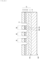
- FIG. 1 illustrates a configuration example of a light emitting device (semiconductor laser 1) according to an embodiment of the present disclosure.
- the semiconductor laser 1 is a laser array in which a plurality of VCSELs is integrated.
- the semiconductor laser 1 has a semiconductor stacked body ST on a first surface 10A of a substrate 10.
- the substrate 10 is a specific example of a "substrate” of the present disclosure.
- the semiconductor stacked body ST is a specific example of a "semiconductor stacked body” of the present disclosure.
- the semiconductor stacked body ST has a buffer layer 11, a first light reflecting layer 12, an active layer 13, a current confining layer 16, and a second light reflecting layer 14 stacked in this order on the first surface 10A of the substrate 10.
- the semiconductor stacked body ST is provided with a first recess 15 in a first recess forming region R15, for example, by performing etching from the second light reflecting layer 14 to a portion of the first light reflecting layer 12. In the region of a portion of the formation region of the first recess 15, the semiconductor stacked body ST is left unetched.
- This provides a plurality (three in the diagram) of mesa regions M1, M2, and M3.
- Each of the mesa regions M1, M2, and M3 has, for example, a columnar shape such as a cylindrical shape.
- a current confining region 16B is formed by the current confining layer 16 with a predetermined width from the outer periphery of the columnar shape.
- the inner portion of the current confining region 16B as viewed from the outer periphery side of the columnar shape is a current injection region 16A.
- the current injection regions 16A of the respective mesa regions M1, M2, and M3 correspond to light emitting regions L1, L2, and L3 of laser beams LT1, LT2, and LT3 (described below).
- Two second recesses 17 are formed on both sides of the first recess forming region R15 of the semiconductor stacked body ST, for example, by performing etching from the second light reflecting layer 14 to a portion of the buffer layer 11.
- the region of a portion of the bottom surface of each of the second recesses 17 has a through opening 18A formed in the buffer layer 11 and the substrate 10.
- An insulating film 22 is formed on the front surface of the semiconductor stacked body ST other than the front surfaces of the semiconductor stacked body ST in the respective mesa regions M1, M2, and M3, the bottom surfaces of the second recesses 17, and the inner wall surfaces of the through openings 18A.
- a through wiring line 19 is formed inside each of the through openings 18A.
- a bottom surface electrically conductive layer 20 is formed on the bottom surface of each of the second recesses 17 to be coupled to the through wiring line 19.
- the through wiring line 19 corresponds to a specific example of a "through wiring line” of the present disclosure.
- An electrode pad 23 is formed from the bottom surface of the second recess 17 to the side wall surface of the second recess 17 and the front surface of the semiconductor stacked body ST to be coupled to the bottom surface electrically conductive layer 20.
- the electrode pad 23 is a specific example of a "first electrically conductive layer" of the present disclosure.
- An n electrode 24 is formed on a second surface 10B of the substrate 10.
- the n electrode 24 is a specific example of a "second electrically conductive layer" of the present disclosure.
- the n electrode 24 is provided to allow a predetermined voltage to be applied to the semiconductor stacked body ST in each of the light emitting regions L1, L2, and L3.
- the n electrode 24 is provided with an opening 24A in association with each of the light emitting regions L1, L2, and L3. It is possible to guide the laser beams LT1, LT2, and LT3 (described below) emitted from the light emitting regions L1, L2, and L3 to the outside from the openings 24A.
- a p electrode 21 is formed on the front surface of the semiconductor stacked body ST in each of the mesa regions M1, M2, and M3.
- FIG. 2 illustrates a planar configuration as viewed from the semiconductor stacked body ST side of the semiconductor laser 1 illustrated in FIG. 1.
- FIG. 1 illustrates a cross-sectional configuration taken along an X-X' line illustrated in FIG. 2.
- FIG. 2 omits the insulating film 22.
- the semiconductor stacked body ST is provided with the first recesses 15 in the first recess forming region R15 to leave the plurality (six in the diagram) of mesa regions M1, M2, M3, M4, M5, and M6.
- FIG. 1 illustrates a cross section that crosses the three mesa regions M1, M2, and M3 of the six mesa regions M1, M2, M3, M4, M5, and M6. As illustrated in FIG.
- the p electrode 21 is formed on the front surface of the semiconductor stacked body ST in each of the mesa regions M1, M2, M3, M4, M5, and M6.
- the plurality (two in the diagram) of second recesses 17 is formed on both sides of the first recess forming region R15 and the through opening 18A is formed in the region of a portion of the bottom surface of each of the second recesses 17.
- the through wiring line 19 is formed inside each of the through openings 18A.
- the electrode pad 23 is formed from the bottom surface of the second recess 17 to the side wall surface of the second recess 17 and the front surface of the semiconductor stacked body ST.
- FIG. 3 illustrates a planar configuration as viewed from the substrate 10 side of the semiconductor laser 1 illustrated in FIG. 1.
- FIG. 1 illustrates a cross-sectional configuration taken along an X-X' line illustrated in FIG. 3 .
- the n electrode 24 is formed on the second surface 10B of the substrate 10. The n electrode 24 is provided with the respective openings 24A in association with the light emitting regions L1, L2, L3, L4, L5, and L6.
- each of the six light emitting regions L1, L2, L3, L4, L5, and L6 is VCSEL.
- the semiconductor laser 1 is a laser array in which six VCSELs are integrated.
- FIGs. 1 to 3 illustrates a configuration in which six VCSELs are integrated, but there is no limitation on the number of VCSELs that are integrated. For example, it is possible to adopt a configuration in which several tens of VCSELs to several thousands of VCSELs are integrated.
- the substrate 10 includes, for example, a gallium arsenide (GaAs) substrate.
- the substrate 10 sometimes includes indium phosphorus (InP), gallium nitride (GaN), silicon (Si), silicon carbide (SiC), or the like through a bonding process or the like of the material system of the light emitting device and a heterogeneous substrate.
- the buffer layer 11 includes, for example, GaAs or the like.
- the buffer layer 11 is provided as a contact layer that electrically couples the substrate 10 and the first light reflecting layer 12.
- the first light reflecting layer 12 is a DBR (Distributed Bragg Reflector) layer disposed between the buffer layer 11 and the active layer 13.
- the first light reflecting layer 12 is opposed to the second light reflecting layer 14 with the active layer 13 and the current confining layer 16 interposed in between.
- the first light reflecting layer 12 is configured to resonate the light generated in the active layer 13 between the first light reflecting layer 12 and the second light reflecting layer 14.
- the first light reflecting layer 12 has a stacked structure in which low refractive index layers and high refractive index layers are alternately stacked on each other.
- a low refractive index layer is n-type Al X1 Ga (1-X1) As (0 ⁇ X1 ⁇ 1) having an optical film thickness of ⁇ /4.
- ⁇ represents the oscillating wavelength of the laser beam emitted from each of the light emitting regions L1, L2, L3, L4, L5, and L6.
- a high refractive index layer is n-type Al X2 Ga (1-X2) As (0 ⁇ X2 ⁇ 1) having an optical film thickness of ⁇ /4.
- the active layer 13 is provided between the first light reflecting layer 12 and the second light reflecting layer 14.
- the active layer 13 includes, for example, an aluminum-gallium-arsenide (AlGaAs) based semiconductor material. This active layer 13 receives a hole (hole) injected from the p electrode 21 via the current injection region 16A and generates induced emission light.
- AlGaAs aluminum-gallium-arsenide
- This active layer 13 receives a hole (hole) injected from the p electrode 21 via the current injection region 16A and generates induced emission light.
- undoped Al X3 Ga (1-X3) As (0 ⁇ X3 ⁇ 1) is usable for the active layer 13.
- the active layer 13 may have a multi quantum well (MQW: Multi Quantum Well) structure of GaAs and AlGaAs, for example.
- the active layer 13 may have a multi quantum well structure of indium gallium arsenide (InGaAs) and AlGaAs.
- the current confining region 16B is formed to have an annular shape with a predetermined width in the current confining layer 16 from the outer periphery side of the columnar shape of each of the mesa regions M1, M2, M3, M4, M5, and M6 to the inner side.
- the inner portion of the current confining region 16B as viewed from the outer periphery side of the columnar shape is the current injection region 16A. It is possible to form the current confining region 16B, for example, by performing an oxidization process on the current confining layer 16 from the outer periphery side of the columnar shape of each of the mesa regions M1, M2, M3, M4, M5, and M6.
- the current confining layer 16 is formed by using, for example, p-type Al X4 Ga (1-X4) As (0.9 ⁇ X4 ⁇ 1).
- the current confining region 16B is formed by oxidizing the current confining layer 16 and includes, for example, aluminum oxide (AlOx).
- the current injection region 16A is a portion that has not been oxidized inside the current confining region 16B.
- the provision of a current confining structure confines electric currents injected into the active layer 13 from the p electrode 21 and increases the current injection efficiency.
- the radius of a substantially circular current injection region 16A is, for example, 1 ⁇ m to 20 ⁇ m.
- the second light reflecting layer 14 is a DBR layer disposed between the current confining layer 16 and the insulating film 22.
- the second light reflecting layer 14 is opposed to the first light reflecting layer 12 with the current confining layer 16 and the active layer 13 interposed in between.
- the second light reflecting layer 14 has a stacked structure in which low refractive index layers and high refractive index layers are alternately stacked on each other.
- a low refractive index layer is n-type Al X5 Ga (1-X5) As (0 ⁇ XS ⁇ 1) having an optical film thickness of X/4.
- a high refractive index layer is n-type Al X6 Ga (1-X6) As (0 ⁇ X6 ⁇ 1) having an optical film thickness of ⁇ /4.
- the insulating film 22 is formed by using, for example, an insulator such as silicon nitride (SiN) or silicon oxide (SiO 2 ).
- the through wiring line 19 is formed by using, for example, a metal such as gold (Au), copper (Cu), or nickel (Ni).
- the bottom surface electrically conductive layer 20 is formed by using, for example, a multilayered film of metals such as gold germanium (AuGe)/nickel/gold.
- the electrode pad 23 is formed by using, for example, a multilayered film of metals such as titanium (Ti)/gold.
- the p electrode 21 is formed by using, for example, a single layer film or a multilayered film of metals such as gold, germanium (Ge), silver (Ag), palladium (Pd), platinum (Pt), nickel, titanium, vanadium (V), tungsten (W), chromium (Cr), aluminum (Al), copper, zinc (Zn), tin (Sn), and indium (In).
- a multilayered film of titanium/platinum/gold is used.
- the n electrode 24 is formed by using, for example, a single layer film or a multilayered film of metals similar to those of the p electrode 21.
- the n electrode 24 may be formed by using a transparent electrode such as ITO (Indium-Tin-Oxide or tin-doped indium oxide), zinc oxide, tin oxide, and titanium oxide. It is possible to include a material and form a pattern for the n electrode 24 in consideration of even thermal conductivity. It is possible to increase the heat dissipation of the substrate 10.
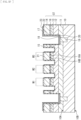
- FIG. 4 illustrates a configuration example of a light emitting apparatus in which the semiconductor laser illustrated in FIG. 1 is mounted on a mounting substrate.
- a light emitting apparatus 3 has a configuration in which the semiconductor laser 1 illustrated in FIG. 1 is flip-chip mounted on a mounting substrate 2.
- the flip-chip mounting is mounting the semiconductor laser 1 with the formation surface of the electrode pad 23 and the p electrode 21 facing the mounting substrate 2.
- the mounting substrate 2 includes, for example, a first electrode 51 and a second electrode 52 on a substrate 50.
- the first electrode 51 is provided to the p electrode 21 of the semiconductor laser 1 and the second electrode 52 is provided to the electrode pad 23 of the semiconductor laser 1 in the respective corresponding patterns.
- the mounting substrate 2 may be provided with a drive circuit such as a power supply circuit for the semiconductor laser 1.
- a terminal of the drive circuit in itself may be configured to be coupled to the p electrode 21 and the electrode pad 23 of the semiconductor laser 1.
- Light generated by recombining an electron and a hole is resonated and amplified between a pair of DBR layers (the first light reflecting layer 12 and the second light reflecting layer 14) and the laser beams LT1, LT2, and LT3 are emitted from the substrate 10 side through the openings 24A.
- a pair of DBR layers the first light reflecting layer 12 and the second light reflecting layer 14
- the laser beams LT1, LT2, and LT3 are emitted from the substrate 10 side through the openings 24A.
- the electrical resistance of the substrate 10 (the voltage drop in a case where the current flows through the substrate 10) sometimes varies the voltages that are applied to the respective light emitting regions L1, L2, and L3. The same applies even in the presence of the light emitting regions L1, L2, and L3 that are different in distance from the n electrode 24.
- the electrical resistance of the substrate 10 (the voltage drop in a case where the current flows through the substrate 10) sometimes varies the voltages that are applied to the respective light emitting regions L1, L2, and L3.
- the n electrode 24 is provided to allow a predetermined voltage to be applied to each of the light emitting regions L1, L2, and L3. This makes it possible to uniformly apply voltages from the n electrode 24 to the respective light emitting regions L1, L2, and L3 in the semiconductor laser 1 regardless of the position of each of the light emitting regions L1, L2, and L3.
- the p electrode 21 is individually provided in each of the light emitting regions L1, L2, and L3.
- the p electrode 21 is individually coupled to the first electrode 51 of the mounting substrate 2. This makes it possible to selectively apply voltages from the p electrode 21 to the light emitting regions L1, L2, and L3 for each of the light emitting regions L1, L2, and L3. In other words, it is possible to performs driving to individually emit the laser beams LT1, LT2, and LT3 from the selected light emitting regions L1, L2, and L3 of the plurality of light emitting regions L1, L2, and L3.
- the configuration has been described in which the laser beams LT1, LT2, and LT3 are emitted through the openings 24A in the semiconductor laser 1, but the present technology is not limited thereto.
- a transparent electrode such as ITO and has transparency to the laser beams LT1, LT2, and LT3
- the laser beams LT1, LT2, and LT3 are not blocked by the n electrode 24. This eliminates the necessity to provide the openings 24A.
- the emission directions of the laser beams LT1, LT2, and LT3 do not have to be the substrate 10 side.
- members such as a wiring line and an electrode each having a light-shielding property are disposed at positions at which the members do not prevent the laser beams LT1, LT2, and LT3 from being emitted.
- the semiconductor laser 1 has a configuration in which the number of electrode pads 23 is smaller than the number of p electrodes 21.
- the p electrode 21 is provided in each of the light emitting regions L1, L2, and L3 as described above and the number of p electrodes 21 thus corresponds to the number of light emitting regions L1, L2, and L3.
- the electrode pad 23 is provided to be coupled to the n electrode 24 that is an electrode common to the plurality of light emitting regions L1, L2, and L3.
- the two electrode pads 23 are provided in the semiconductor laser 1. It is sufficient if the number of electrode pads 23 is at least one and it is possible to include a smaller number of electrode pads 23 than the number of p electrodes 21. A smaller number of electrode pads 23 are preferable because a smaller number of electrode pads 23 simplify the configuration of the semiconductor laser 1 more and facilitate the manufacturing.
- FIGs. 5A to 5H illustrates a step in the method of manufacturing the semiconductor laser 1.
- the buffer layer 11, the first light reflecting layer 12, the active layer 13, the current confining layer 16, and the second light reflecting layer 14 are stacked in this order on the substrate 10 to form the semiconductor stacked body ST.
- the semiconductor stacked body ST is formed through epitaxial crystal growth using, for example, a molecular beam epitaxy (MBE: Molecular Beam Epitaxy) method, a metal organic chemical vapor deposition (MOCVD: Metal Organic Chemical Vapor Deposition) method, or the like.
- MBE molecular beam epitaxy
- MOCVD Metal Organic Chemical Vapor Deposition
- a resist film (not illustrated) having a predetermined pattern is patterned and formed in an upper layer of the semiconductor stacked body ST in a photolithography step.
- Etching is performed from the second light reflecting layer 14 to a portion of the first light reflecting layer 12 for removal to form the first recess 15.
- the etching is performed, for example, by reactive ion etching (RIE: Reactive Ion Etching).
- RIE reactive ion etching
- the resist film described above is formed to have a pattern for protecting the mesa regions M1, M2, and M3. This leaves the semiconductor stacked body ST having a columnar shape in the mesa regions M1, M2, and M3 in the etching process described above. Subsequently, the resist film is removed.
- a resist film (not illustrated) having a predetermined pattern is patterned and formed in an upper layer of the semiconductor stacked body ST to form the second recess 17 by performing etching such as RIE from the second light reflecting layer 14 to a portion of the buffer layer 11 for removal.
- etching such as RIE from the second light reflecting layer 14 to a portion of the buffer layer 11 for removal.
- the resist film is removed.
- a resist film (not illustrated) having a predetermined pattern is patterned and formed in an upper layer of the semiconductor stacked body ST to form the through wiring line recess 18 by performing etching such as RIE up to a portion of the substrate 10 on a portion of the bottom of the second recess 17 for removal.
- etching such as RIE up to a portion of the substrate 10 on a portion of the bottom of the second recess 17 for removal.
- the resist film is removed.
- the insulating film 22 of silicon nitride or the like is formed, for example, in a chemical vapor deposition (CVD: Chemical Vapor Deposition) method or an atomic layer deposition (ALD: Atomic Layer Deposition) method.
- CVD Chemical Vapor Deposition
- ALD Atomic Layer Deposition
- the insulating film 22 is formed to cover the inner wall surface of the first recess 15 and the inner wall surface of the second recess 17.
- a resist film (not illustrated) having a predetermined pattern is patterned and formed in an upper layer of the semiconductor stacked body ST and etching such as RIE is performed to remove the insulating film 22 on the front surface of the semiconductor stacked body ST in each of the mesa regions M1, M2, and M3, the bottom surface of the second recess 17, and the inner wall surface of a through wiring line recess 18 of the front surface of the semiconductor stacked body ST.
- gold or the like is embedded inside the through wiring line recess 18 , for example, by an electroplating process or the like to form the through wiring line 19.
- the bottom surface electrically conductive layer 20 is formed by forming a multilayered film of the metals of AuGe/Ni/Au at the bottom of the second recess 17, for example, in a metal deposition method or the like.
- the p electrode 21 is formed by forming a multilayered film of the metals of Ti/Pt/Au on the front surface of the semiconductor stacked body ST in each of the mesa regions M1, M2, and M3, for example, in a sputtering method or the like.
- the electrode pad 23 is formed to be coupled to the bottom surface electrically conductive layer 20 by forming a multilayered film of the metals of Ti/Au from the bottom surface of the second recess 17 to the side wall surface of the second recess 17 and the front surface of the semiconductor stacked body ST, for example, in a sputtering method or the like.
- the second surface 10B of the substrate 10 is polished, for example, by a chemical mechanical polishing (Chemical Mechanical Polishing) process until the through wiring line 19 is exposed.
- a chemical mechanical polishing Chemical Mechanical Polishing
- the n electrode 24 is formed by forming a multilayered film of the metals of AuGe/Ni/Au on the second surface 10B of the substrate 10, for example, in a metal deposition method or the like.
- the n electrode 24 is provided with the openings 24A corresponding to the light emitting regions L1, L2, and L3 in the respective mesa regions M1, M2, and M3 to complete the semiconductor laser 1.
- the operation of the semiconductor laser 1 according to the present embodiment is described with reference to FIG. 1 .
- voltages are applied to the semiconductor stacked body ST in each of the mesa regions M1, M2, and M3 from the p electrode 21 and the n electrode 24.
- This injects an electron from the n electrode 24 and injects a hole from the p electrode 21 in each of the light emitting regions L1, L2, and L3.
- the recombination of the electron and the hole generates light.
- the light is resonated and amplified between a pair of DBR layers and the laser beams LT1, LT2, and LT3 are emitted from the substrate 10 side through the openings 24A.
- the n electrode 24 is provided to allow a predetermined voltage to be applied to the second surface of the substrate 10 in each of the light emitting regions L1, L2, and L3.
- the electrode pad 23 is coupled to the n electrode 24 via the through wiring line 19. It is possible to apply a voltage to the n electrode 24 from the electrode pad 23 provided on the second surface 10B of the substrate 10.
- the n electrode 24 is provided to allow a predetermined voltage to be applied to the second surface of the substrate 10 in each of the light emitting regions L1, L2, and L3.
- the application of a voltage to the n electrode 24 makes it possible to uniformly apply voltages to the light emitting regions L1, L2, and L3 regardless of the position of each of the light emitting regions L1, L2, and L3.
- the semiconductor laser 1 is provided with the p electrode 21 and the electrode pad 23 on the same surface (second surface 10B) as that of the substrate 10 and it is thus possible to flip-chip mount the semiconductor laser 1.
- the semiconductor laser 1 is individually provided with the p electrode 21 for each of the light emitting regions L1, L2, and L3. This makes it possible to perform driving to individually emit the laser beams LT1, LT2, and LT3 from the selected light emitting regions L1, L2, and L3 of the light emitting regions L1, L2, and L3.
- the semiconductor laser 1 prefferably includes a material and form a pattern for the n electrode 24 in consideration of even thermal conductivity. It is possible to increase the heat dissipation of the substrate 10.
- the semiconductor laser including six VCSELs has been described in the embodiment described above, but this is not limitative. It is also possible to apply this, for example, to a semiconductor laser in which several tens of VCSELs to several thousands of VCSELs are integrated instead.
- the distance between the light emitting region of each laser and the n electrode sometimes varies more as a larger number of lasers are integrated.
- the present technology makes it possible to apply a voltage to the light emitting region of each laser with a voltage difference suppressed to be small.
- the present technology is applicable to a variety of electronic apparatuses including a semiconductor laser.
- the present technology is applicable to a light source included in a portable electronic apparatus such as a smartphone, a light source of each of a variety of sensing apparatuses that each sense a shape, an operation, and the like, or the like.
- present technology may be configured as below.
- the present technology having the following configurations makes it possible to uniformly apply voltages to a semiconductor stacked body in a plurality of light emitting regions. This makes it possible to obtain uniform light emission characteristics between the plurality of light emitting regions.
Landscapes
- Physics & Mathematics (AREA)
- Condensed Matter Physics & Semiconductors (AREA)
- General Physics & Mathematics (AREA)
- Electromagnetism (AREA)
- Optics & Photonics (AREA)
- Semiconductor Lasers (AREA)
Claims (10)
- Lichtemittierende Vorrichtung (1), umfassend:ein Substrat (10), das eine erste Oberfläche (10A) und eine zweite Oberfläche aufweist, die einander entgegengesetzt sind;einen gestapelten Halbleiterkörper (ST), der auf der ersten Oberfläche des Substrats bereitgestellt ist, wobei der gestapelte Halbleiterkörper eine Vielzahl von lichtemittierenden Bereichen (L1, L2, L3) aufweist, von denen jeder ermöglicht, dass ein Laserstrahl emittiert wird;eine erste elektrisch leitfähige Schicht (23), die auf einer vorderen Oberfläche des gestapelten Halbleiterkörpers bereitgestellt ist, wobei die vordere Oberfläche dem Substrat gegenüberliegt;eine zweite elektrisch leitfähige Schicht (24), die auf der zweiten Oberfläche des Substrats bereitgestellt ist, wobei die zweite elektrisch leitfähige Schicht bereitgestellt ist, um zu ermöglichen, dass eine vorbestimmte Spannung an den gestapelten Halbleiterkörper in jedem einer Vielzahl von lichtemittierenden Bereichen angelegt wird;eine Durchverdrahtungsleitung (19), die die erste elektrisch leitfähige Schicht und die zweite elektrisch leitfähige Schicht elektrisch koppelt; undeine Vielzahl von Elektroden (21), die auf der vorderen Oberfläche des gestapelten Halbleiterkörpers bereitgestellt ist, wobei die vordere Oberfläche dem Substrat gegenüberliegt, wobei die Vielzahl von Elektroden bereitgestellt ist, um zu ermöglichen, dass vorbestimmte Spannungen an den gestapelten Halbleiterkörper in einer Vielzahl der jeweiligen lichtemittierenden Bereiche angelegt werden.
- Lichtemittierende Vorrichtung nach Anspruch 1, wobei der gestapelte Halbleiterkörper eine erste lichtreflektierende Schicht (12), eine aktive Schicht (13) und eine zweite lichtreflektierende Schicht (14), die in einer Reihenfolge von der Substratseite gestapelt ist, aufweist.
- Lichtemittierende Vorrichtung nach Anspruch 2, wobei der gestapelte Halbleiterkörper ferner eine Strombegrenzungsschicht (16) zwischen der aktiven Schicht und der zweiten lichtreflektierenden Schicht einschließt, wobei die Strombegrenzungsschicht einen Stromeinspeisungsbereich (16A) aufweist.
- Lichtemittierende Vorrichtung nach einem der Ansprüche 1 bis 3, wobei der gestapelte Halbleiterkörper eine Vielzahl von Mesabereichen (M1, M2, M3) aufweist, die jeweils eine Vielzahl der lichtemittierenden Bereiche einschließen.
- Lichtemittierende Vorrichtung nach Anspruch 1, wobei es eine Vielzahl von ersten elektrisch leitfähigen Schichten gibt, die die erste elektrisch leitfähige Schicht einschließen; und eine Anzahl der Vielzahl von ersten elektrisch leitfähigen Schichten kleiner als eine Anzahl der Elektroden ist.
- Lichtemittierende Vorrichtung nach einem der Ansprüche 1 bis 5, wobei jeder von einer Vielzahl der lichtemittierenden Bereiche den Laserstrahl von der Substratseite emittiert.
- Lichtemittierende Vorrichtung nach Anspruch 6, wobei die zweite elektrisch leitfähige Schicht eine Vielzahl von Öffnungen aufweist, die in Verbindung mit einer Vielzahl der lichtemittierenden Bereiche bereitgestellt ist, wobei die Vielzahl von Öffnungen jeweils den Laserstrahl führen.
- Lichtemittierende Vorrichtung nach Anspruch 6, wobei die zweite elektrisch leitfähige Schicht eine elektrisch leitfähige Schicht einschließt, die eine Transparenz für den Laserstrahl aufweist.
- Lichtemittierende Vorrichtung nach einem der Ansprüche 1 bis 8, wobei die lichtemittierende Vorrichtung ein Flip-Chip ist, der auf einem Montagesubstrat von einer Seite montiert ist, auf der die erste elektrisch leitfähige Schicht bereitgestellt ist.
- Lichtemittierende Einrichtung, umfassend
eine lichtemittierende Vorrichtung nach Anspruch 1, die ein Flip-Chip ist, der auf einem Montagesubstrat montiert ist.
Applications Claiming Priority (2)
| Application Number | Priority Date | Filing Date | Title |
|---|---|---|---|
| JP2018216958 | 2018-11-20 | ||
| PCT/JP2019/043223 WO2020105411A1 (ja) | 2018-11-20 | 2019-11-05 | 発光デバイス及び発光装置 |
Publications (3)
| Publication Number | Publication Date |
|---|---|
| EP3886274A1 EP3886274A1 (de) | 2021-09-29 |
| EP3886274A4 EP3886274A4 (de) | 2022-02-23 |
| EP3886274B1 true EP3886274B1 (de) | 2024-06-12 |
Family
ID=70773496
Family Applications (1)
| Application Number | Title | Priority Date | Filing Date |
|---|---|---|---|
| EP19886228.6A Active EP3886274B1 (de) | 2018-11-20 | 2019-11-05 | Lichtemittierende vorrichtung und lichtemittierende einrichtung |
Country Status (4)
| Country | Link |
|---|---|
| US (1) | US20210391689A1 (de) |
| EP (1) | EP3886274B1 (de) |
| JP (1) | JP7353299B2 (de) |
| WO (1) | WO2020105411A1 (de) |
Families Citing this family (6)
| Publication number | Priority date | Publication date | Assignee | Title |
|---|---|---|---|---|
| TWI701882B (zh) * | 2018-11-08 | 2020-08-11 | 晶智達光電股份有限公司 | 雷射元件 |
| WO2021196368A1 (en) * | 2020-04-02 | 2021-10-07 | Shenzhen Raysees AI Technology Co., Ltd. | Bottom-emitting multijunction vcsel array |
| JP2022044477A (ja) * | 2020-09-07 | 2022-03-17 | 富士フイルムビジネスイノベーション株式会社 | 発光素子 |
| JP7707605B2 (ja) * | 2021-03-29 | 2025-07-15 | セイコーエプソン株式会社 | 発光装置、プロジェクター、およびディスプレイ |
| CN113783105B (zh) * | 2021-09-07 | 2022-11-01 | 常州纵慧芯光半导体科技有限公司 | 一种垂直腔面发射激光器及其制备方法 |
| CN121336329A (zh) * | 2023-06-28 | 2026-01-13 | 索尼半导体解决方案公司 | 表面发射装置及表面发射装置的制造方法 |
Family Cites Families (15)
| Publication number | Priority date | Publication date | Assignee | Title |
|---|---|---|---|---|
| US6023485A (en) * | 1998-02-17 | 2000-02-08 | Motorola, Inc. | Vertical cavity surface emitting laser array with integrated photodetector |
| US6753199B2 (en) * | 2001-06-29 | 2004-06-22 | Xanoptix, Inc. | Topside active optical device apparatus and method |
| JP3962240B2 (ja) * | 2001-10-31 | 2007-08-22 | 株式会社日立製作所 | 近接場光プローブ集積半導体レーザ及びそれを用いた光記録装置 |
| JP5212686B2 (ja) * | 2007-08-22 | 2013-06-19 | ソニー株式会社 | 半導体レーザアレイの製造方法 |
| JP2011029339A (ja) * | 2009-07-23 | 2011-02-10 | Sony Corp | 半導体素子およびその製造方法 |
| JP5621369B2 (ja) * | 2010-07-12 | 2014-11-12 | 株式会社リコー | 面発光レーザ素子、光走査装置及び画像形成装置 |
| JP5803545B2 (ja) * | 2011-10-12 | 2015-11-04 | ソニー株式会社 | 半導体レーザ素子、光電変換装置および光情報処理装置 |
| US8675706B2 (en) * | 2011-12-24 | 2014-03-18 | Princeton Optronics Inc. | Optical illuminator |
| KR20140134701A (ko) * | 2012-03-14 | 2014-11-24 | 코닌클리케 필립스 엔.브이. | Vcsel 모듈 및 그것의 제조 |
| JP2015103783A (ja) * | 2013-11-28 | 2015-06-04 | キヤノン株式会社 | 発光素子アレイ |
| US10153615B2 (en) * | 2015-07-30 | 2018-12-11 | Optipulse, Inc. | Rigid high power and high speed lasing grid structures |
| JP6743436B2 (ja) * | 2016-03-17 | 2020-08-19 | 株式会社リコー | 面発光レーザアレイ、及びレーザ装置 |
| JP2017216285A (ja) | 2016-05-30 | 2017-12-07 | 株式会社リコー | 面発光レーザアレイ素子、光源ユニット及びレーザ装置 |
| JP2018021695A (ja) | 2016-08-02 | 2018-02-08 | ニチバン株式会社 | 冷蔵庫ヒートパイプ固定用粘着テープ |
| JP6308319B2 (ja) | 2017-04-20 | 2018-04-11 | 富士ゼロックス株式会社 | 面発光型半導体レーザアレイ |
-
2019
- 2019-11-05 JP JP2020558236A patent/JP7353299B2/ja active Active
- 2019-11-05 EP EP19886228.6A patent/EP3886274B1/de active Active
- 2019-11-05 WO PCT/JP2019/043223 patent/WO2020105411A1/ja not_active Ceased
- 2019-11-05 US US17/286,985 patent/US20210391689A1/en not_active Abandoned
Also Published As
| Publication number | Publication date |
|---|---|
| WO2020105411A1 (ja) | 2020-05-28 |
| US20210391689A1 (en) | 2021-12-16 |
| EP3886274A1 (de) | 2021-09-29 |
| EP3886274A4 (de) | 2022-02-23 |
| JP7353299B2 (ja) | 2023-09-29 |
| JPWO2020105411A1 (ja) | 2021-10-14 |
Similar Documents
| Publication | Publication Date | Title |
|---|---|---|
| EP3886274B1 (de) | Lichtemittierende vorrichtung und lichtemittierende einrichtung | |
| JP6176298B2 (ja) | 面発光型半導体レーザアレイ及び面発光型半導体レーザアレイの製造方法 | |
| CN101136538B (zh) | Vcsel、其制造方法、模块、光发送装置、光空间传输装置、光发送系统以及光空间传输系统 | |
| JP6216785B2 (ja) | キャビティ内コンタクトを有するvcsel | |
| EP2684263B1 (de) | Vcsel-array mit erhöhter effizienz | |
| CN111564754A (zh) | 垂直腔面发射激光器 | |
| US20230246420A1 (en) | Surface-emitting semiconductor laser | |
| EP1488484A2 (de) | Hybrider vertikalresonatorlaser mit vergrabener grenzfläche | |
| EP1746694B1 (de) | Vcsel mit querlaufendem p/n Übergang | |
| WO2007105328A1 (ja) | 面発光レーザ素子アレイ | |
| JP4087152B2 (ja) | 面発光半導体レーザ素子及びレーザアレイ | |
| JP3785683B2 (ja) | 面発光素子 | |
| US11165222B2 (en) | Optically matched vertical-cavity surface-emitting laser (VCSEL) with passivation | |
| JP6724961B2 (ja) | 発光素子アレイ | |
| JP2018082061A (ja) | 発光素子アレイ、および光伝送装置 | |
| JP4879094B2 (ja) | 半導体発光素子及びその製造方法 | |
| US20220158413A1 (en) | Semiconductor laser | |
| US7440481B2 (en) | Surface-emitting type semiconductor laser and method for manufacturing the same | |
| US20250007247A1 (en) | Vertical cavity surface emitting laser device with dual wavelength bands | |
| JP2005166870A (ja) | 光素子及びその製造方法、光モジュール、光伝送装置 | |
| TW202448056A (zh) | 面發光雷射元件 | |
| JP2018182154A (ja) | 面発光型半導体発光素子およびその製造方法 | |
| KR20190064380A (ko) | 광 소자 |
Legal Events
| Date | Code | Title | Description |
|---|---|---|---|
| STAA | Information on the status of an ep patent application or granted ep patent |
Free format text: STATUS: THE INTERNATIONAL PUBLICATION HAS BEEN MADE |
|
| PUAI | Public reference made under article 153(3) epc to a published international application that has entered the european phase |
Free format text: ORIGINAL CODE: 0009012 |
|
| STAA | Information on the status of an ep patent application or granted ep patent |
Free format text: STATUS: REQUEST FOR EXAMINATION WAS MADE |
|
| 17P | Request for examination filed |
Effective date: 20210506 |
|
| AK | Designated contracting states |
Kind code of ref document: A1 Designated state(s): AL AT BE BG CH CY CZ DE DK EE ES FI FR GB GR HR HU IE IS IT LI LT LU LV MC MK MT NL NO PL PT RO RS SE SI SK SM TR |
|
| A4 | Supplementary search report drawn up and despatched |
Effective date: 20220124 |
|
| DAV | Request for validation of the european patent (deleted) | ||
| DAX | Request for extension of the european patent (deleted) | ||
| RIC1 | Information provided on ipc code assigned before grant |
Ipc: H01S 5/183 20060101ALI20220118BHEP Ipc: H01S 5/42 20060101AFI20220118BHEP |
|
| GRAP | Despatch of communication of intention to grant a patent |
Free format text: ORIGINAL CODE: EPIDOSNIGR1 |
|
| STAA | Information on the status of an ep patent application or granted ep patent |
Free format text: STATUS: GRANT OF PATENT IS INTENDED |
|
| INTG | Intention to grant announced |
Effective date: 20240115 |
|
| P01 | Opt-out of the competence of the unified patent court (upc) registered |
Effective date: 20240206 |
|
| GRAS | Grant fee paid |
Free format text: ORIGINAL CODE: EPIDOSNIGR3 |
|
| GRAA | (expected) grant |
Free format text: ORIGINAL CODE: 0009210 |
|
| STAA | Information on the status of an ep patent application or granted ep patent |
Free format text: STATUS: THE PATENT HAS BEEN GRANTED |
|
| AK | Designated contracting states |
Kind code of ref document: B1 Designated state(s): AL AT BE BG CH CY CZ DE DK EE ES FI FR GB GR HR HU IE IS IT LI LT LU LV MC MK MT NL NO PL PT RO RS SE SI SK SM TR |
|
| REG | Reference to a national code |
Ref country code: GB Ref legal event code: FG4D |
|
| REG | Reference to a national code |
Ref country code: CH Ref legal event code: EP |
|
| REG | Reference to a national code |
Ref country code: IE Ref legal event code: FG4D |
|
| REG | Reference to a national code |
Ref country code: DE Ref legal event code: R096 Ref document number: 602019053742 Country of ref document: DE |
|
| PG25 | Lapsed in a contracting state [announced via postgrant information from national office to epo] |
Ref country code: BG Free format text: LAPSE BECAUSE OF FAILURE TO SUBMIT A TRANSLATION OF THE DESCRIPTION OR TO PAY THE FEE WITHIN THE PRESCRIBED TIME-LIMIT Effective date: 20240612 |
|
| PG25 | Lapsed in a contracting state [announced via postgrant information from national office to epo] |
Ref country code: FI Free format text: LAPSE BECAUSE OF FAILURE TO SUBMIT A TRANSLATION OF THE DESCRIPTION OR TO PAY THE FEE WITHIN THE PRESCRIBED TIME-LIMIT Effective date: 20240612 Ref country code: HR Free format text: LAPSE BECAUSE OF FAILURE TO SUBMIT A TRANSLATION OF THE DESCRIPTION OR TO PAY THE FEE WITHIN THE PRESCRIBED TIME-LIMIT Effective date: 20240612 |
|
| REG | Reference to a national code |
Ref country code: LT Ref legal event code: MG9D |
|
| PG25 | Lapsed in a contracting state [announced via postgrant information from national office to epo] |
Ref country code: GR Free format text: LAPSE BECAUSE OF FAILURE TO SUBMIT A TRANSLATION OF THE DESCRIPTION OR TO PAY THE FEE WITHIN THE PRESCRIBED TIME-LIMIT Effective date: 20240913 |
|
| REG | Reference to a national code |
Ref country code: NL Ref legal event code: MP Effective date: 20240612 |
|
| PG25 | Lapsed in a contracting state [announced via postgrant information from national office to epo] |
Ref country code: ES Free format text: LAPSE BECAUSE OF FAILURE TO SUBMIT A TRANSLATION OF THE DESCRIPTION OR TO PAY THE FEE WITHIN THE PRESCRIBED TIME-LIMIT Effective date: 20240612 |
|
| PG25 | Lapsed in a contracting state [announced via postgrant information from national office to epo] |
Ref country code: LV Free format text: LAPSE BECAUSE OF FAILURE TO SUBMIT A TRANSLATION OF THE DESCRIPTION OR TO PAY THE FEE WITHIN THE PRESCRIBED TIME-LIMIT Effective date: 20240612 |
|
| PG25 | Lapsed in a contracting state [announced via postgrant information from national office to epo] |
Ref country code: NO Free format text: LAPSE BECAUSE OF FAILURE TO SUBMIT A TRANSLATION OF THE DESCRIPTION OR TO PAY THE FEE WITHIN THE PRESCRIBED TIME-LIMIT Effective date: 20240912 Ref country code: LV Free format text: LAPSE BECAUSE OF FAILURE TO SUBMIT A TRANSLATION OF THE DESCRIPTION OR TO PAY THE FEE WITHIN THE PRESCRIBED TIME-LIMIT Effective date: 20240612 Ref country code: HR Free format text: LAPSE BECAUSE OF FAILURE TO SUBMIT A TRANSLATION OF THE DESCRIPTION OR TO PAY THE FEE WITHIN THE PRESCRIBED TIME-LIMIT Effective date: 20240612 Ref country code: GR Free format text: LAPSE BECAUSE OF FAILURE TO SUBMIT A TRANSLATION OF THE DESCRIPTION OR TO PAY THE FEE WITHIN THE PRESCRIBED TIME-LIMIT Effective date: 20240913 Ref country code: FI Free format text: LAPSE BECAUSE OF FAILURE TO SUBMIT A TRANSLATION OF THE DESCRIPTION OR TO PAY THE FEE WITHIN THE PRESCRIBED TIME-LIMIT Effective date: 20240612 Ref country code: ES Free format text: LAPSE BECAUSE OF FAILURE TO SUBMIT A TRANSLATION OF THE DESCRIPTION OR TO PAY THE FEE WITHIN THE PRESCRIBED TIME-LIMIT Effective date: 20240612 Ref country code: BG Free format text: LAPSE BECAUSE OF FAILURE TO SUBMIT A TRANSLATION OF THE DESCRIPTION OR TO PAY THE FEE WITHIN THE PRESCRIBED TIME-LIMIT Effective date: 20240612 Ref country code: RS Free format text: LAPSE BECAUSE OF FAILURE TO SUBMIT A TRANSLATION OF THE DESCRIPTION OR TO PAY THE FEE WITHIN THE PRESCRIBED TIME-LIMIT Effective date: 20240912 |
|
| PG25 | Lapsed in a contracting state [announced via postgrant information from national office to epo] |
Ref country code: NL Free format text: LAPSE BECAUSE OF FAILURE TO SUBMIT A TRANSLATION OF THE DESCRIPTION OR TO PAY THE FEE WITHIN THE PRESCRIBED TIME-LIMIT Effective date: 20240612 |
|
| REG | Reference to a national code |
Ref country code: AT Ref legal event code: MK05 Ref document number: 1695031 Country of ref document: AT Kind code of ref document: T Effective date: 20240612 |
|
| PG25 | Lapsed in a contracting state [announced via postgrant information from national office to epo] |
Ref country code: NL Free format text: LAPSE BECAUSE OF FAILURE TO SUBMIT A TRANSLATION OF THE DESCRIPTION OR TO PAY THE FEE WITHIN THE PRESCRIBED TIME-LIMIT Effective date: 20240612 |
|
| PG25 | Lapsed in a contracting state [announced via postgrant information from national office to epo] |
Ref country code: PT Free format text: LAPSE BECAUSE OF FAILURE TO SUBMIT A TRANSLATION OF THE DESCRIPTION OR TO PAY THE FEE WITHIN THE PRESCRIBED TIME-LIMIT Effective date: 20241014 |
|
| PG25 | Lapsed in a contracting state [announced via postgrant information from national office to epo] |
Ref country code: PT Free format text: LAPSE BECAUSE OF FAILURE TO SUBMIT A TRANSLATION OF THE DESCRIPTION OR TO PAY THE FEE WITHIN THE PRESCRIBED TIME-LIMIT Effective date: 20241014 |
|
| PGFP | Annual fee paid to national office [announced via postgrant information from national office to epo] |
Ref country code: DE Payment date: 20241022 Year of fee payment: 6 |
|
| PG25 | Lapsed in a contracting state [announced via postgrant information from national office to epo] |
Ref country code: PL Free format text: LAPSE BECAUSE OF FAILURE TO SUBMIT A TRANSLATION OF THE DESCRIPTION OR TO PAY THE FEE WITHIN THE PRESCRIBED TIME-LIMIT Effective date: 20240612 |
|
| PGFP | Annual fee paid to national office [announced via postgrant information from national office to epo] |
Ref country code: GB Payment date: 20241023 Year of fee payment: 6 |
|
| PG25 | Lapsed in a contracting state [announced via postgrant information from national office to epo] |
Ref country code: EE Free format text: LAPSE BECAUSE OF FAILURE TO SUBMIT A TRANSLATION OF THE DESCRIPTION OR TO PAY THE FEE WITHIN THE PRESCRIBED TIME-LIMIT Effective date: 20240612 |
|
| PG25 | Lapsed in a contracting state [announced via postgrant information from national office to epo] |
Ref country code: AT Free format text: LAPSE BECAUSE OF FAILURE TO SUBMIT A TRANSLATION OF THE DESCRIPTION OR TO PAY THE FEE WITHIN THE PRESCRIBED TIME-LIMIT Effective date: 20240612 Ref country code: IS Free format text: LAPSE BECAUSE OF FAILURE TO SUBMIT A TRANSLATION OF THE DESCRIPTION OR TO PAY THE FEE WITHIN THE PRESCRIBED TIME-LIMIT Effective date: 20241012 |
|
| PG25 | Lapsed in a contracting state [announced via postgrant information from national office to epo] |
Ref country code: CZ Free format text: LAPSE BECAUSE OF FAILURE TO SUBMIT A TRANSLATION OF THE DESCRIPTION OR TO PAY THE FEE WITHIN THE PRESCRIBED TIME-LIMIT Effective date: 20240612 |
|
| PG25 | Lapsed in a contracting state [announced via postgrant information from national office to epo] |
Ref country code: SK Free format text: LAPSE BECAUSE OF FAILURE TO SUBMIT A TRANSLATION OF THE DESCRIPTION OR TO PAY THE FEE WITHIN THE PRESCRIBED TIME-LIMIT Effective date: 20240612 Ref country code: RO Free format text: LAPSE BECAUSE OF FAILURE TO SUBMIT A TRANSLATION OF THE DESCRIPTION OR TO PAY THE FEE WITHIN THE PRESCRIBED TIME-LIMIT Effective date: 20240612 |
|
| PG25 | Lapsed in a contracting state [announced via postgrant information from national office to epo] |
Ref country code: SM Free format text: LAPSE BECAUSE OF FAILURE TO SUBMIT A TRANSLATION OF THE DESCRIPTION OR TO PAY THE FEE WITHIN THE PRESCRIBED TIME-LIMIT Effective date: 20240612 |
|
| PG25 | Lapsed in a contracting state [announced via postgrant information from national office to epo] |
Ref country code: SM Free format text: LAPSE BECAUSE OF FAILURE TO SUBMIT A TRANSLATION OF THE DESCRIPTION OR TO PAY THE FEE WITHIN THE PRESCRIBED TIME-LIMIT Effective date: 20240612 Ref country code: SK Free format text: LAPSE BECAUSE OF FAILURE TO SUBMIT A TRANSLATION OF THE DESCRIPTION OR TO PAY THE FEE WITHIN THE PRESCRIBED TIME-LIMIT Effective date: 20240612 Ref country code: RO Free format text: LAPSE BECAUSE OF FAILURE TO SUBMIT A TRANSLATION OF THE DESCRIPTION OR TO PAY THE FEE WITHIN THE PRESCRIBED TIME-LIMIT Effective date: 20240612 Ref country code: PL Free format text: LAPSE BECAUSE OF FAILURE TO SUBMIT A TRANSLATION OF THE DESCRIPTION OR TO PAY THE FEE WITHIN THE PRESCRIBED TIME-LIMIT Effective date: 20240612 Ref country code: IS Free format text: LAPSE BECAUSE OF FAILURE TO SUBMIT A TRANSLATION OF THE DESCRIPTION OR TO PAY THE FEE WITHIN THE PRESCRIBED TIME-LIMIT Effective date: 20241012 Ref country code: EE Free format text: LAPSE BECAUSE OF FAILURE TO SUBMIT A TRANSLATION OF THE DESCRIPTION OR TO PAY THE FEE WITHIN THE PRESCRIBED TIME-LIMIT Effective date: 20240612 Ref country code: CZ Free format text: LAPSE BECAUSE OF FAILURE TO SUBMIT A TRANSLATION OF THE DESCRIPTION OR TO PAY THE FEE WITHIN THE PRESCRIBED TIME-LIMIT Effective date: 20240612 Ref country code: AT Free format text: LAPSE BECAUSE OF FAILURE TO SUBMIT A TRANSLATION OF THE DESCRIPTION OR TO PAY THE FEE WITHIN THE PRESCRIBED TIME-LIMIT Effective date: 20240612 |
|
| PG25 | Lapsed in a contracting state [announced via postgrant information from national office to epo] |
Ref country code: IT Free format text: LAPSE BECAUSE OF FAILURE TO SUBMIT A TRANSLATION OF THE DESCRIPTION OR TO PAY THE FEE WITHIN THE PRESCRIBED TIME-LIMIT Effective date: 20240612 |
|
| REG | Reference to a national code |
Ref country code: DE Ref legal event code: R097 Ref document number: 602019053742 Country of ref document: DE |
|
| PG25 | Lapsed in a contracting state [announced via postgrant information from national office to epo] |
Ref country code: DK Free format text: LAPSE BECAUSE OF FAILURE TO SUBMIT A TRANSLATION OF THE DESCRIPTION OR TO PAY THE FEE WITHIN THE PRESCRIBED TIME-LIMIT Effective date: 20240612 |
|
| PLBE | No opposition filed within time limit |
Free format text: ORIGINAL CODE: 0009261 |
|
| STAA | Information on the status of an ep patent application or granted ep patent |
Free format text: STATUS: NO OPPOSITION FILED WITHIN TIME LIMIT |
|
| 26N | No opposition filed |
Effective date: 20250313 |
|
| REG | Reference to a national code |
Ref country code: CH Ref legal event code: PL |
|
| PG25 | Lapsed in a contracting state [announced via postgrant information from national office to epo] |
Ref country code: MC Free format text: LAPSE BECAUSE OF FAILURE TO SUBMIT A TRANSLATION OF THE DESCRIPTION OR TO PAY THE FEE WITHIN THE PRESCRIBED TIME-LIMIT Effective date: 20240612 |
|
| PG25 | Lapsed in a contracting state [announced via postgrant information from national office to epo] |
Ref country code: LU Free format text: LAPSE BECAUSE OF NON-PAYMENT OF DUE FEES Effective date: 20241105 |
|
| REG | Reference to a national code |
Ref country code: CH Ref legal event code: PL |
|
| PG25 | Lapsed in a contracting state [announced via postgrant information from national office to epo] |
Ref country code: CH Free format text: LAPSE BECAUSE OF NON-PAYMENT OF DUE FEES Effective date: 20241130 |
|
| REG | Reference to a national code |
Ref country code: BE Ref legal event code: MM Effective date: 20241130 |
|
| PG25 | Lapsed in a contracting state [announced via postgrant information from national office to epo] |
Ref country code: SE Free format text: LAPSE BECAUSE OF FAILURE TO SUBMIT A TRANSLATION OF THE DESCRIPTION OR TO PAY THE FEE WITHIN THE PRESCRIBED TIME-LIMIT Effective date: 20240612 |
|
| PG25 | Lapsed in a contracting state [announced via postgrant information from national office to epo] |
Ref country code: BE Free format text: LAPSE BECAUSE OF NON-PAYMENT OF DUE FEES Effective date: 20241130 |
|
| PG25 | Lapsed in a contracting state [announced via postgrant information from national office to epo] |
Ref country code: FR Free format text: LAPSE BECAUSE OF NON-PAYMENT OF DUE FEES Effective date: 20241130 |
|
| PG25 | Lapsed in a contracting state [announced via postgrant information from national office to epo] |
Ref country code: IE Free format text: LAPSE BECAUSE OF NON-PAYMENT OF DUE FEES Effective date: 20241105 |
|
| PG25 | Lapsed in a contracting state [announced via postgrant information from national office to epo] |
Ref country code: HU Free format text: LAPSE BECAUSE OF FAILURE TO SUBMIT A TRANSLATION OF THE DESCRIPTION OR TO PAY THE FEE WITHIN THE PRESCRIBED TIME-LIMIT; INVALID AB INITIO Effective date: 20191105 |
|
| PG25 | Lapsed in a contracting state [announced via postgrant information from national office to epo] |
Ref country code: CY Free format text: LAPSE BECAUSE OF FAILURE TO SUBMIT A TRANSLATION OF THE DESCRIPTION OR TO PAY THE FEE WITHIN THE PRESCRIBED TIME-LIMIT; INVALID AB INITIO Effective date: 20191105 |