EP3886545A1 - Gehäuse und elektronische vorrichtung - Google Patents
Gehäuse und elektronische vorrichtung Download PDFInfo
- Publication number
- EP3886545A1 EP3886545A1 EP19929748.2A EP19929748A EP3886545A1 EP 3886545 A1 EP3886545 A1 EP 3886545A1 EP 19929748 A EP19929748 A EP 19929748A EP 3886545 A1 EP3886545 A1 EP 3886545A1
- Authority
- EP
- European Patent Office
- Prior art keywords
- connector
- housing
- connection ring
- connection
- main body
- Prior art date
- Legal status (The legal status is an assumption and is not a legal conclusion. Google has not performed a legal analysis and makes no representation as to the accuracy of the status listed.)
- Granted
Links
Images




Classifications
-
- H—ELECTRICITY
- H01—ELECTRIC ELEMENTS
- H01R—ELECTRICALLY-CONDUCTIVE CONNECTIONS; STRUCTURAL ASSOCIATIONS OF A PLURALITY OF MUTUALLY-INSULATED ELECTRICAL CONNECTING ELEMENTS; COUPLING DEVICES; CURRENT COLLECTORS
- H01R13/00—Details of coupling devices of the kinds covered by groups H01R12/70 or H01R24/00 - H01R33/00
- H01R13/648—Protective earth or shield arrangements on coupling devices, e.g. anti-static shielding
-
- H—ELECTRICITY
- H05—ELECTRIC TECHNIQUES NOT OTHERWISE PROVIDED FOR
- H05K—PRINTED CIRCUITS; CASINGS OR CONSTRUCTIONAL DETAILS OF ELECTRIC APPARATUS; MANUFACTURE OF ASSEMBLAGES OF ELECTRICAL COMPONENTS
- H05K9/00—Screening of apparatus or components against electric or magnetic fields
- H05K9/0007—Casings
- H05K9/0018—Casings with provisions to reduce aperture leakages in walls, e.g. terminals, connectors, cables
-
- H—ELECTRICITY
- H01—ELECTRIC ELEMENTS
- H01R—ELECTRICALLY-CONDUCTIVE CONNECTIONS; STRUCTURAL ASSOCIATIONS OF A PLURALITY OF MUTUALLY-INSULATED ELECTRICAL CONNECTING ELEMENTS; COUPLING DEVICES; CURRENT COLLECTORS
- H01R13/00—Details of coupling devices of the kinds covered by groups H01R12/70 or H01R24/00 - H01R33/00
- H01R13/73—Means for mounting coupling parts to apparatus or structures, e.g. to a wall
-
- H—ELECTRICITY
- H05—ELECTRIC TECHNIQUES NOT OTHERWISE PROVIDED FOR
- H05K—PRINTED CIRCUITS; CASINGS OR CONSTRUCTIONAL DETAILS OF ELECTRIC APPARATUS; MANUFACTURE OF ASSEMBLAGES OF ELECTRICAL COMPONENTS
- H05K5/00—Casings, cabinets or drawers for electric apparatus
- H05K5/0026—Casings, cabinets or drawers for electric apparatus provided with connectors and printed circuit boards [PCB], e.g. automotive electronic control units
- H05K5/0069—Casings, cabinets or drawers for electric apparatus provided with connectors and printed circuit boards [PCB], e.g. automotive electronic control units having connector relating features for connecting the connector pins with the PCB or for mounting the connector body with the housing
-
- H—ELECTRICITY
- H05—ELECTRIC TECHNIQUES NOT OTHERWISE PROVIDED FOR
- H05K—PRINTED CIRCUITS; CASINGS OR CONSTRUCTIONAL DETAILS OF ELECTRIC APPARATUS; MANUFACTURE OF ASSEMBLAGES OF ELECTRICAL COMPONENTS
- H05K5/00—Casings, cabinets or drawers for electric apparatus
- H05K5/02—Details
- H05K5/0247—Electrical details of casings, e.g. terminals, passages for cables or wiring
-
- H—ELECTRICITY
- H05—ELECTRIC TECHNIQUES NOT OTHERWISE PROVIDED FOR
- H05K—PRINTED CIRCUITS; CASINGS OR CONSTRUCTIONAL DETAILS OF ELECTRIC APPARATUS; MANUFACTURE OF ASSEMBLAGES OF ELECTRICAL COMPONENTS
- H05K5/00—Casings, cabinets or drawers for electric apparatus
- H05K5/06—Hermetically-sealed casings
- H05K5/069—Other details of the casing, e.g. wall structure, passage for a connector, a cable, a shaft
-
- H—ELECTRICITY
- H05—ELECTRIC TECHNIQUES NOT OTHERWISE PROVIDED FOR
- H05K—PRINTED CIRCUITS; CASINGS OR CONSTRUCTIONAL DETAILS OF ELECTRIC APPARATUS; MANUFACTURE OF ASSEMBLAGES OF ELECTRICAL COMPONENTS
- H05K9/00—Screening of apparatus or components against electric or magnetic fields
- H05K9/0007—Casings
- H05K9/002—Casings with localised screening
-
- G—PHYSICS
- G02—OPTICS
- G02B—OPTICAL ELEMENTS, SYSTEMS OR APPARATUS
- G02B6/00—Light guides; Structural details of arrangements comprising light guides and other optical elements, e.g. couplings
- G02B6/24—Coupling light guides
- G02B6/36—Mechanical coupling means
- G02B6/38—Mechanical coupling means having fibre to fibre mating means
- G02B6/3807—Dismountable connectors, i.e. comprising plugs
- G02B6/3897—Connectors fixed to housings, casing, frames or circuit boards
-
- G—PHYSICS
- G02—OPTICS
- G02B—OPTICAL ELEMENTS, SYSTEMS OR APPARATUS
- G02B6/00—Light guides; Structural details of arrangements comprising light guides and other optical elements, e.g. couplings
- G02B6/24—Coupling light guides
- G02B6/42—Coupling light guides with opto-electronic elements
- G02B6/4292—Coupling light guides with opto-electronic elements the light guide being disconnectable from the opto-electronic element, e.g. mutually self aligning arrangements
Definitions
- This application relates to the field of electronic device technologies, and in particular, to a housing and an electronic device.
- a function of a connector is to build a communication bridge between blocked or isolated circuits in a circuit to transmit electric energy, electrical signals, and optical signals.
- a connector usually needs to be installed, and a connection to another electronic device is implemented by using the connector.
- a boss structure usually needs to be disposed on a housing of the electronic device to provide an installation location for the connector.
- the disposing of the boss structure increases a weight of the housing of the electronic device, and also increases a volume of the electronic device. This is not conducive to a lightweight and miniaturized design.
- a flange structure is usually disposed on an outer housing of the connector. Therefore, a size of the boss structure is further increased.
- installation by using the screw is relatively complex, and therefore is not conducive to automated assembly.
- a conventional connector housing usually includes an outer housing, an inner housing, and a metallic shielding case located between the outer housing and the inner housing. This is not conducive to production, manufacturing costs are relatively high, and continuity and airtightness of shielding are not ensured.
- This application provides a housing and an electronic device that have a simple and compact structure and on which a connector can be easily installed.
- this application provides a housing, including a main body and a connection ring.
- the main body has a via.
- the connection ring is disposed on one side of the main body and is connected to the via.
- the connection ring is configured to connect to a connector.
- the connection ring encloses shielding space for accommodating the connector.
- the housing may provide an installation location or accommodation space for an electrical element, to protect the electrical element. Because the electrical element installed in the housing needs to be photoelectrically connected to an external device or electrical element by using the connector, the connector needs to be installed on the housing.
- the connector may be fastened to the housing by using the connection ring, and is accommodated in the shielding space enclosed by the connection ring, to prevent electromagnetic interference between the connector and another electrical element or electronic device.
- the via facilitates routing of a cable, to implement a photoelectric connection between the connector and the electronic element.
- the electrical element may also be photoelectrically connected to another electrical element by using the connector, to implement a connection between the electronic element installed in the housing and another device or electronic element.
- the photoelectric connection may include an electrical connection for transmitting an electrical signal and electric energy, and may also include an optical connection for transmitting an optical signal.
- a boss structure used to install the connector does not need to be additionally disposed on the housing, so that a weight and a volume of the housing can be reduced.
- a technological process for assembling the connector and the housing can be further simplified. This reduces manufacturing costs, improves assembly efficiency, and facilitates automated assembly.
- the connection ring can provide the shielding space for the connector. This helps simplify a structure of the connector, without additionally disposing a shielding structure on the connector, thereby reducing manufacturing costs of the connector.
- the housing may be an integrated structure.
- the housing may be manufactured by using a casting molding process.
- the main body and the connection ring of the housing may be separately molded, and then the molded main body and connection ring are connected by using a process such as welding or bonding.
- connection ring may be further connected to an external connector.
- connection ring has a first connection part and a second connection part.
- the first connection part is configured to connect to a first connector
- the second connection part is configured to connect to a second connector.
- the first connector is photoelectrically connected to the electrical element installed in the housing
- the second connector is photoelectrically connected to another device. After the first connector is connected to the second connector, the electrical element installed in the housing can be photoelectrically connected to the another device.
- connection ring and the connector There may be a plurality of connection manners between the connection ring and the connector.
- the connection ring and the connector are connected by using a clamping structure.
- first connection part and the second connection part may be clamp locks.
- a clamp lock structure used to connect to the first connection part is also disposed in the first connector
- a clamp lock structure used to connect to the second connection part is also disposed in the second connector.
- connection ring In addition, to improve structural strength of the connection ring, in some embodiments, at least one reinforcing rib may be disposed on the connection ring.
- connection ring may be made of a metallic material. Therefore, an effective shielding function can be provided to protect the connector against interference from an electromagnetic signal, or prevent an electromagnetic signal generated by the connector from affecting another electrical element.
- connection ring may be alternatively made of a non-metallic material, to reduce manufacturing costs and a weight of the housing.
- a shield layer may be disposed in the connection ring, so that the connection ring also has a shielding function.
- this application further provides an electronic device, including the housing according to any one of the foregoing implementations and an electrical element installed in the main body, and further including a connector.
- the connector is connected to the connection ring and is photoelectrically connected to the electrical element.
- connection ring may be disposed inside the housing, or may be disposed outside the housing.
- the connection ring does not occupy inner space of the housing.
- a volume occupied by the entire electronic device can be reduced, and an outer contour of the electronic device can also be flat.
- connection ring also has a shielding function
- a shielding structure may be omitted from the connector.
- the connector includes an insulator and a connection piece.
- the insulator is configured to connect to the connection ring.
- the connection piece is disposed in the insulator and is photoelectrically connected to the electrical element.
- a structure of the connector can be simplified, thereby reducing manufacturing costs of the connector, and ensuring continuity and stability of shielding.
- the electronic device further includes a sealing element.
- the sealing element may be disposed between the insulator of the connector and the connection ring, or may be disposed between the insulator of the connector and the main body of the housing.
- the sealing element may be disposed between the insulator of the connector and an inner wall of the connection ring.
- the sealing element may be disposed between the insulator of the connector and the main body.
- an inner cross-sectional contour of the connection ring is larger than a cross-sectional contour of the via, to facilitate sealing between the insulator of the connector and the main body.
- an embodiment or “some embodiments” or the like in this specification means that one or more embodiments of this application include a specific feature, structure, or characteristic described with reference to the embodiment. Therefore, a statement such as “in an embodiment”, “in some embodiments”, “in some other embodiments”, or “in some other embodiments” that appears along with a difference in the specification does not necessarily mean referring to a same embodiment, but means “one or more but not all embodiments", unless otherwise particularly emphasized in another manner.
- the terms “include”, “comprise”, “have”, and their variants all mean “including but not limited to", unless otherwise particularly emphasized in another manner.
- the housing in the embodiments of this application is used in an electronic device, to provide an installing location or accommodation space for an electrical element in the electronic device, to protect the electrical element.
- the electronic device may be specifically a power distribution unit (power distribution unit, PDU), an on-board controller (on-board controller, OBC), an optical fiber distribution box (optical fiber distribution box, ODB), or the like. Because photoelectric transmission needs to be performed between electronic devices or between an electronic device and an electrical element, to improve convenience and stability of a connection, connectors are widely used.
- connectors There are various types of connectors, but their functions are very simple, that is, to build a communication bridge between blocked or isolated circuits in a circuit, so that a current flows and the circuit implements an intended function.
- the connector not merely connects the current.
- the connector can also perform a function of connecting an optical signal.
- a connector is usually installed on a housing of the electronic device.
- a connection ring can not only implement installing of the connector, but also provide a corresponding function (for example, a shielding function) according to an actual requirement. Therefore, the housing in this application has benefits such as a simple structure and a wide application scope.
- a technological process for assembling the connector and the housing can be simplified, and even a structure of the connector can be simplified. This reduces manufacturing costs, improves assembly efficiency, and facilitates automated assembly.
- the housing may have a plurality of connection rings, and a cross-sectional contour of the connection ring may be a polygonal structure such as a circle, a rectangle, or a triangle.
- the connection ring and a main body may be an integrated structure or split structures. Specifically, when the connection ring and the main body are an integrated structure, a casting process or the like may be used for manufacturing. When the connection ring and the main body are split structures, the connection ring and the main body may be first manufactured and molded separately, and then the connection ring and the main body are connected by using a connection manner such as welding or bonding.
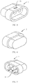
- connection ring 12 is in a rounded rectangular shape
- the housing 1 is an integrated structure, that is, the main body 11 and the connection ring 12 are an integrated structure.
- connection ring 12 has a first connection part 121.
- connection manner such as clamping or a threaded connection may be used between the connection ring 12 and the connector.
- the connection manner of clamping is used between the connection ring 12 and the connector.
- the first connection part 121 is a clamp lock disposed inside the connection ring 12, and the clamp lock is a rectangular slot.
- a clamp lock structure for clamping with the first connection part 121 is also disposed in the connector.
- the clamp lock structure may be a protrusion clamped with the rectangular slot.
- connectors are usually used in pairs. Specifically, the connector installed on the connection ring needs to be connected to another connector.
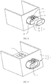
- first connector 2 As shown in FIG. 3 to FIG. 5 , for ease of understanding, two connectors connected to each other are described as a first connector 2 and a second connector 3.
- the first connector 2 is installed on the connection ring 12 of the housing 1 by using the clamp lock structure 21, and is photoelectrically connected to an electrical element installed in the housing.
- the second connector 3 is a connector connected to another electronic device. Only a photoelectric connection may be implemented between the first connector 2 and the second connector 3, or a mechanical connection may be implemented between the first connector 2 and the second connector 3 in addition to a photoelectric connection.
- connection ring 12 when only the photoelectric connection is implemented between the first connector 2 and the second connector 3, to prevent the first connector 2 from detaching from the second connector 3 under external force, as shown in FIG. 1 , in the embodiment provided in this application, the connection ring 12 further has a second connection part 122 configured to connect to the second connector 2.
- the connection ring 12 may be connected not only to the first connector 2, but also to the second connector 3.
- the second connection part 122 may be a clamp lock structure.
- a clamp lock structure 31 used for clamping with the second connection part is also disposed in the second connector 3.
- the clamp lock structure 122 provided in this application is a right-angled triangular protrusion, a right-angled surface is disposed toward the main body 11, and the inclined surface is disposed away from the main body 11.
- the clamp lock structure 31 in the second connector is a rectangular slot.
- the mechanical connection can be further implemented between the first connector and the second connector in addition to the photoelectric connection, to prevent the first connector from detaching from the second connector under external force.
- the mechanical connection between the first connector and the second connector may be implemented in a plurality of manners.
- the first connector and the second connector may be connected in a manner such as clamping or a threaded connection.
- clamping portions that are to be clamped with each other should be disposed on the first connector and the second connector.
- threaded structures should be disposed on the first connector and the second connector.
- a shielding structure needs to be disposed, to prevent electromagnetic interference between the connector and the electronic device.
- connection ring 12 is made of a metallic material. After the first connector 2 is fixedly installed in the connection ring 12, the connection ring 12 may provide a shielding function for the first connector 2, to prevent electromagnetic interference between the electrical element located in the housing 1 and the first connector 2, or prevent electromagnetic interference between another electronic device outside the housing 1 and the first connector 2.
- materials of both the connection ring 12 and the main body 11 may be metallic materials; or a non-metallic material such as plastic is used for the main body 11, and a metallic material is used for the connection ring 12.
- the housing 1 may be manufactured by using a casting process; or the connection ring 12 and the main body 11 are separately manufactured, and then the connection ring 12 and the main body 11 are connected by using a process such as welding or bonding.
- connection ring 12 When the main body 11 is made of a plastic material and the connection ring 12 is made of a metallic material, the connection ring 12 may be first molded, and then the main body 11 is molded by using an in-mold injection molding process. In addition, the main body 11 and the connection ring 12 are combined. Certainly, the connection ring 12 and the main body 11 may be alternatively connected in a manner such as bonding or a threaded connection.
- connection ring 12 includes a body 125 and a shield layershield layer 123.
- the shield layer 123 is made of a metallic material, and the body 125 may be made of a non-metallic material such as plastic. This structural setting enables the connection ring 12 to have a shielding function and a wider range of material selection, and a manufacturing process and material selection for the entire housing 1 can also be more flexible.
- the main body 11 of the housing 1 and the body 125 of the connection ring 12 may be made of a same plastic material, so that the main body 11 of the housing 1 and the body 125 of the connection ring 12 may be injection-molded by using an injection molding process. Then the molded shield layer 123 may be fixed to the body 125 of the connection ring 12.
- the shield layer 123 may be specifically a metallic ring, and the shield layer 123 may be specifically fixed to the body 125 of the connection ring 12 in a plurality of manners.
- bonding For example, bonding, clamping, or a threaded connection may be used.
- the shield layer 123 may be alternatively a metallic film molded on the body 125.
- a metallic material may be directly molded on the body of the connection ring by using a process such as evaporation or spray coating, to form the shield layer 123.
- connection ring 12 In addition, to improve structural strength of the connection ring 12, as shown in FIG. 1 and FIG. 7 , in the embodiment provided in this application, at least one reinforcing rib 124 is disposed on an outer wall of the connection ring 12.
- the reinforcing rib 124 is a long strip structure extending along a length direction of the connection ring, and is distributed on an outer peripheral surface of the connection ring.
- the reinforcing rib 124 may alternatively extend to a junction between the connection ring 12 and the main body 11.
- an embodiment of this application further provides an electronic device, including the housing 1 in any one of the foregoing embodiments and an electrical element 4 installed in the main body 11, and further including a connector 2.
- the connector 2 is connected to the connection ring 12, and is photoelectrically connected to the electrical element 4.
- the electronic device may be specifically a power distribution unit (power distribution unit, PDU), an on-board controller (on-board controller, OBC), an optical fiber distribution box (optical fiber distribution box, ODB), or the like.
- the electrical element may be specifically an optical cable, a printed circuit board (print circuit board), or the like.
- connection ring 12 may be disposed inside the housing 1, or may be disposed outside the housing 1. As shown in FIG. 11 , when the connection ring is disposed outside the housing 1, the connection ring does not occupy inner space of the housing 1. As shown in FIG. 12 , when the connection ring 12 is disposed inside the housing, a volume occupied by the entire electronic device can be reduced, and an outer contour of the electronic device can also be flat. Therefore, space occupied by the electronic device can be reduced, thereby facilitating logistics transportation.
- connection ring 12 also has a shielding function
- a shielding structure may be omitted from the connector 2.
- the connector 2 includes an insulator 22 and a connection piece 23.
- the insulator 22 is configured to connect to the connection ring 12.
- the connection piece 23 is disposed in the insulator 22 and is photoelectrically connected to the electrical element 4.
- a structure of the connector 2 can be simplified, thereby reducing manufacturing costs of the connector 2, and ensuring continuity and stability of shielding.
- the electronic device further includes a sealing element 5.
- the sealing element 5 may be disposed between the insulator 22 of the connector 2 and the connection ring 12, or may be disposed between the insulator 22 of the connector 2 and the main body 11 of the housing 1.
- the sealing element 5 may be disposed between the insulator 22 of the connector 2 and an inner wall of the connection ring 12.
- the annular sealing element 5 may be sleeved on an outer periphery of the insulator 22. After the connector 2 is installed in the connection ring 12, the outer periphery of the sealing element 5 is closely attached to the inner wall of the connection ring 12, to implement sealing between the housing 1 and the connector 2.
- the sealing element 5 may be alternatively attached to the main body 11 of the housing 1 in an airtight manner.
- the sealing element 5 may be attached to an inner wall of a via 111 in an airtight manner, or the sealing element 5 may be attached to an outer wall of the main body 11 in an airtight manner.
- an inner cross-sectional contour of the connection ring 12 is larger than a cross-sectional contour of the via 111, so that a sufficient contact area can be reserved between the inner wall of the connection ring 12 and the via 111 for attaching the sealing element 5, to facilitate sealing between the insulator 22 of the connector 2 and the main body 11.
- a specific material of the sealing element 5 may be nitrile rubber, silicone rubber, fluorosilicone rubber, or the like.
Landscapes
- Engineering & Computer Science (AREA)
- Microelectronics & Electronic Packaging (AREA)
- Connector Housings Or Holding Contact Members (AREA)
- Casings For Electric Apparatus (AREA)
Applications Claiming Priority (2)
| Application Number | Priority Date | Filing Date | Title |
|---|---|---|---|
| CN201910420107.4A CN110324998B (zh) | 2019-05-20 | 2019-05-20 | 一种壳体及电子设备 |
| PCT/CN2019/128027 WO2020233115A1 (zh) | 2019-05-20 | 2019-12-24 | 一种壳体及电子设备 |
Publications (3)
| Publication Number | Publication Date |
|---|---|
| EP3886545A1 true EP3886545A1 (de) | 2021-09-29 |
| EP3886545A4 EP3886545A4 (de) | 2022-04-20 |
| EP3886545B1 EP3886545B1 (de) | 2023-10-25 |
Family
ID=68113146
Family Applications (1)
| Application Number | Title | Priority Date | Filing Date |
|---|---|---|---|
| EP19929748.2A Active EP3886545B1 (de) | 2019-05-20 | 2019-12-24 | Gehäuse und elektronische vorrichtung |
Country Status (4)
| Country | Link |
|---|---|
| EP (1) | EP3886545B1 (de) |
| JP (1) | JP7234387B2 (de) |
| CN (1) | CN110324998B (de) |
| WO (1) | WO2020233115A1 (de) |
Cited By (1)
| Publication number | Priority date | Publication date | Assignee | Title |
|---|---|---|---|---|
| WO2023088661A3 (en) * | 2021-11-16 | 2023-06-29 | Belimo Holding Ag | Modular electrical interface |
Families Citing this family (3)
| Publication number | Priority date | Publication date | Assignee | Title |
|---|---|---|---|---|
| CN110324998B (zh) * | 2019-05-20 | 2021-02-26 | 华为技术有限公司 | 一种壳体及电子设备 |
| CN113939119A (zh) * | 2021-09-01 | 2022-01-14 | 浙江零跑科技股份有限公司 | 一种母线输入装置 |
| CN115377720B (zh) * | 2022-07-27 | 2026-03-27 | 华为数字能源技术有限公司 | 连接器、供电系统及车辆 |
Family Cites Families (25)
| Publication number | Priority date | Publication date | Assignee | Title |
|---|---|---|---|---|
| US6482017B1 (en) | 2000-02-10 | 2002-11-19 | Infineon Technologies North America Corp. | EMI-shielding strain relief cable boot and dust cover |
| US20020025722A1 (en) * | 2000-08-04 | 2002-02-28 | Hideho Inagawa | Shielded cable with connector |
| JP4309121B2 (ja) | 2002-12-19 | 2009-08-05 | Necインフロンティア株式会社 | シールドケーブルのノイズ抑制構造 |
| CN2742604Y (zh) * | 2004-09-17 | 2005-11-23 | 连展科技(深圳)有限公司 | 连接器套壳结构 |
| US7234950B1 (en) * | 2006-04-26 | 2007-06-26 | Robert Bosch Gmbh | Electrical connector assembly |
| JP5624805B2 (ja) * | 2010-06-10 | 2014-11-12 | 矢崎総業株式会社 | シールド端末接続構造及び方法 |
| JP5806523B2 (ja) * | 2011-06-24 | 2015-11-10 | 矢崎総業株式会社 | グロメット付きコネクタ |
| CN102856745A (zh) * | 2011-06-30 | 2013-01-02 | 鸿富锦精密工业(深圳)有限公司 | 电连接器及其电子装置 |
| JP5744092B2 (ja) * | 2013-03-22 | 2015-07-01 | 三菱電機株式会社 | 電子制御装置および電子制御装置の製造方法 |
| US9099820B2 (en) * | 2013-09-18 | 2015-08-04 | Delphi Technologies, Inc. | Electronics module with a side entry connection |
| DE102013221239B4 (de) * | 2013-10-21 | 2021-10-07 | Zf Friedrichshafen Ag | Steuerungseinrichtung |
| JP6163089B2 (ja) * | 2013-11-20 | 2017-07-12 | 矢崎総業株式会社 | シールド構造、シールドシェル及び電線付きシールドコネクタの製造方法 |
| CN104953350B (zh) * | 2014-03-31 | 2017-07-25 | 富士康(昆山)电脑接插件有限公司 | 信号传输模块 |
| TWM497868U (zh) * | 2014-12-05 | 2015-03-21 | Simula Technology Inc | 利用塗膠平面塗佈防水膠之防水連接器 |
| CN204885586U (zh) * | 2015-08-19 | 2015-12-16 | 东莞市好润精密电子有限公司 | 一种汽车发动机连接器端子外壳塑胶件 |
| CN205282669U (zh) * | 2015-11-05 | 2016-06-01 | 香港商安费诺(东亚)有限公司 | 能垂直定位于电子装置中的带线连接器 |
| CN107293895B (zh) * | 2016-04-11 | 2019-07-26 | 富士康(昆山)电脑接插件有限公司 | 电连接器及其制造方法 |
| CN206893889U (zh) * | 2017-03-31 | 2018-01-16 | 深圳市创亿欣精密电子股份有限公司 | 一种摄像头防水连接结构 |
| CN207664355U (zh) * | 2017-11-22 | 2018-07-27 | 深圳市沃尔新能源电气科技股份有限公司 | 屏蔽罩和电连接器 |
| CN208797292U (zh) * | 2018-04-18 | 2019-04-26 | 泰科电子(上海)有限公司 | 连接器组件 |
| CN208209041U (zh) * | 2018-06-14 | 2018-12-07 | 郑志锋 | 一种用于快速连接电缆的精密连接器 |
| EP3629429B1 (de) * | 2018-09-25 | 2024-11-06 | Apple Inc. | Io-integration mit schwimmenden verbindern in einem netz |
| CN208862262U (zh) * | 2018-09-26 | 2019-05-14 | 深圳市西多利精密实业有限公司 | 一种带有座体的防水连接器 |
| CN112397915B (zh) * | 2018-12-31 | 2021-09-07 | 深圳北芯生命科技股份有限公司 | 插件式连接装置 |
| CN110324998B (zh) * | 2019-05-20 | 2021-02-26 | 华为技术有限公司 | 一种壳体及电子设备 |
-
2019
- 2019-05-20 CN CN201910420107.4A patent/CN110324998B/zh active Active
- 2019-12-24 EP EP19929748.2A patent/EP3886545B1/de active Active
- 2019-12-24 WO PCT/CN2019/128027 patent/WO2020233115A1/zh not_active Ceased
- 2019-12-24 JP JP2021544639A patent/JP7234387B2/ja active Active
Cited By (1)
| Publication number | Priority date | Publication date | Assignee | Title |
|---|---|---|---|---|
| WO2023088661A3 (en) * | 2021-11-16 | 2023-06-29 | Belimo Holding Ag | Modular electrical interface |
Also Published As
| Publication number | Publication date |
|---|---|
| CN110324998B (zh) | 2021-02-26 |
| CN110324998A (zh) | 2019-10-11 |
| EP3886545B1 (de) | 2023-10-25 |
| JP2022519548A (ja) | 2022-03-24 |
| EP3886545A4 (de) | 2022-04-20 |
| WO2020233115A1 (zh) | 2020-11-26 |
| JP7234387B2 (ja) | 2023-03-07 |
Similar Documents
| Publication | Publication Date | Title |
|---|---|---|
| EP3886545A1 (de) | Gehäuse und elektronische vorrichtung | |
| US8992249B2 (en) | Shielded connector | |
| US11515673B2 (en) | Electrical connector module with shielding members engaging upon connection to a mating connector | |
| EP3430797B1 (de) | Kameraanordnung mit abgeschirmter bildgeberschaltung | |
| CN103477509B (zh) | 屏蔽连接器 | |
| KR102468410B1 (ko) | 카메라 모듈 | |
| CN107040229B (zh) | 用于高压连接器装配件的滤波器组件和高压连接器装配件 | |
| US9590321B2 (en) | Cable connection structure of camera module for vehicle | |
| CN108695640A (zh) | 密封构件及电连接器 | |
| US20250219335A1 (en) | Connector and electronic device | |
| JP2018045836A (ja) | コネクタ | |
| EP3656602B1 (de) | Kondensatoreinheit für system zur kontaktlosen stromübertragung | |
| KR20180103656A (ko) | 전기 커넥터의 부착구조 및 전기 커넥터 모듈의 제조방법 | |
| EP3557698B1 (de) | Verbinderbaugruppe | |
| JP2022519548A5 (de) | ||
| US9190768B2 (en) | Connector having a first seal and a second seal and a pressing rib | |
| WO2022268017A1 (zh) | 电子设备 | |
| WO2022260038A1 (ja) | 電気コネクタ・ユニット | |
| EP3989365B1 (de) | Batterieverbindungsvorrichtung | |
| CN113310530B (zh) | 集成式电机温度和角度传感器 | |
| CN113381181A (zh) | 摄像机 | |
| CN212694387U (zh) | 用于固定电学部件的壳体及触摸屏装置 | |
| CN113615020A (zh) | 温度异常检测装置 | |
| CN218830227U (zh) | 一种图像处理组件、摄像头模组及电子设备 | |
| CN215732390U (zh) | 一种驱动设备、照明组件及车辆 |
Legal Events
| Date | Code | Title | Description |
|---|---|---|---|
| STAA | Information on the status of an ep patent application or granted ep patent |
Free format text: STATUS: THE INTERNATIONAL PUBLICATION HAS BEEN MADE |
|
| PUAI | Public reference made under article 153(3) epc to a published international application that has entered the european phase |
Free format text: ORIGINAL CODE: 0009012 |
|
| STAA | Information on the status of an ep patent application or granted ep patent |
Free format text: STATUS: REQUEST FOR EXAMINATION WAS MADE |
|
| 17P | Request for examination filed |
Effective date: 20210624 |
|
| AK | Designated contracting states |
Kind code of ref document: A1 Designated state(s): AL AT BE BG CH CY CZ DE DK EE ES FI FR GB GR HR HU IE IS IT LI LT LU LV MC MK MT NL NO PL PT RO RS SE SI SK SM TR |
|
| RAP3 | Party data changed (applicant data changed or rights of an application transferred) |
Owner name: HUAWEI DIGITL POWER TECHNOLOGIES CO., LTD. |
|
| RAP1 | Party data changed (applicant data changed or rights of an application transferred) |
Owner name: HUAWEI DIGITAL POWER TECHNOLOGIES CO., LTD. |
|
| A4 | Supplementary search report drawn up and despatched |
Effective date: 20220321 |
|
| RIC1 | Information provided on ipc code assigned before grant |
Ipc: H05K 5/06 20060101ALI20220315BHEP Ipc: H05K 5/00 20060101ALI20220315BHEP Ipc: H05K 9/00 20060101ALI20220315BHEP Ipc: H05K 5/02 20060101AFI20220315BHEP |
|
| STAA | Information on the status of an ep patent application or granted ep patent |
Free format text: STATUS: EXAMINATION IS IN PROGRESS |
|
| DAV | Request for validation of the european patent (deleted) | ||
| DAX | Request for extension of the european patent (deleted) | ||
| 17Q | First examination report despatched |
Effective date: 20220817 |
|
| GRAP | Despatch of communication of intention to grant a patent |
Free format text: ORIGINAL CODE: EPIDOSNIGR1 |
|
| STAA | Information on the status of an ep patent application or granted ep patent |
Free format text: STATUS: GRANT OF PATENT IS INTENDED |
|
| RIC1 | Information provided on ipc code assigned before grant |
Ipc: G02B 6/42 20060101ALN20230523BHEP Ipc: G02B 6/38 20060101ALN20230523BHEP Ipc: H05K 5/06 20060101ALI20230523BHEP Ipc: H05K 5/00 20060101ALI20230523BHEP Ipc: H05K 9/00 20060101ALI20230523BHEP Ipc: H05K 5/02 20060101AFI20230523BHEP |
|
| RIC1 | Information provided on ipc code assigned before grant |
Ipc: G02B 6/42 20060101ALN20230526BHEP Ipc: G02B 6/38 20060101ALN20230526BHEP Ipc: H05K 5/06 20060101ALI20230526BHEP Ipc: H05K 5/00 20060101ALI20230526BHEP Ipc: H05K 9/00 20060101ALI20230526BHEP Ipc: H05K 5/02 20060101AFI20230526BHEP |
|
| INTG | Intention to grant announced |
Effective date: 20230615 |
|
| P01 | Opt-out of the competence of the unified patent court (upc) registered |
Effective date: 20230727 |
|
| GRAS | Grant fee paid |
Free format text: ORIGINAL CODE: EPIDOSNIGR3 |
|
| GRAA | (expected) grant |
Free format text: ORIGINAL CODE: 0009210 |
|
| STAA | Information on the status of an ep patent application or granted ep patent |
Free format text: STATUS: THE PATENT HAS BEEN GRANTED |
|
| AK | Designated contracting states |
Kind code of ref document: B1 Designated state(s): AL AT BE BG CH CY CZ DE DK EE ES FI FR GB GR HR HU IE IS IT LI LT LU LV MC MK MT NL NO PL PT RO RS SE SI SK SM TR |
|
| REG | Reference to a national code |
Ref country code: GB Ref legal event code: FG4D |
|
| REG | Reference to a national code |
Ref country code: CH Ref legal event code: EP |
|
| REG | Reference to a national code |
Ref country code: DE Ref legal event code: R096 Ref document number: 602019040357 Country of ref document: DE |
|
| REG | Reference to a national code |
Ref country code: IE Ref legal event code: FG4D |
|
| REG | Reference to a national code |
Ref country code: LT Ref legal event code: MG9D |
|
| REG | Reference to a national code |
Ref country code: NL Ref legal event code: MP Effective date: 20231025 |
|
| REG | Reference to a national code |
Ref country code: AT Ref legal event code: MK05 Ref document number: 1626065 Country of ref document: AT Kind code of ref document: T Effective date: 20231025 |
|
| PG25 | Lapsed in a contracting state [announced via postgrant information from national office to epo] |
Ref country code: NL Free format text: LAPSE BECAUSE OF FAILURE TO SUBMIT A TRANSLATION OF THE DESCRIPTION OR TO PAY THE FEE WITHIN THE PRESCRIBED TIME-LIMIT Effective date: 20231025 |
|
| PG25 | Lapsed in a contracting state [announced via postgrant information from national office to epo] |
Ref country code: GR Free format text: LAPSE BECAUSE OF FAILURE TO SUBMIT A TRANSLATION OF THE DESCRIPTION OR TO PAY THE FEE WITHIN THE PRESCRIBED TIME-LIMIT Effective date: 20240126 |
|
| PG25 | Lapsed in a contracting state [announced via postgrant information from national office to epo] |
Ref country code: IS Free format text: LAPSE BECAUSE OF FAILURE TO SUBMIT A TRANSLATION OF THE DESCRIPTION OR TO PAY THE FEE WITHIN THE PRESCRIBED TIME-LIMIT Effective date: 20240225 |
|
| PG25 | Lapsed in a contracting state [announced via postgrant information from national office to epo] |
Ref country code: LT Free format text: LAPSE BECAUSE OF FAILURE TO SUBMIT A TRANSLATION OF THE DESCRIPTION OR TO PAY THE FEE WITHIN THE PRESCRIBED TIME-LIMIT Effective date: 20231025 |
|
| PG25 | Lapsed in a contracting state [announced via postgrant information from national office to epo] |
Ref country code: AT Free format text: LAPSE BECAUSE OF FAILURE TO SUBMIT A TRANSLATION OF THE DESCRIPTION OR TO PAY THE FEE WITHIN THE PRESCRIBED TIME-LIMIT Effective date: 20231025 |
|
| PG25 | Lapsed in a contracting state [announced via postgrant information from national office to epo] |
Ref country code: ES Free format text: LAPSE BECAUSE OF FAILURE TO SUBMIT A TRANSLATION OF THE DESCRIPTION OR TO PAY THE FEE WITHIN THE PRESCRIBED TIME-LIMIT Effective date: 20231025 |
|
| PG25 | Lapsed in a contracting state [announced via postgrant information from national office to epo] |
Ref country code: LT Free format text: LAPSE BECAUSE OF FAILURE TO SUBMIT A TRANSLATION OF THE DESCRIPTION OR TO PAY THE FEE WITHIN THE PRESCRIBED TIME-LIMIT Effective date: 20231025 Ref country code: IS Free format text: LAPSE BECAUSE OF FAILURE TO SUBMIT A TRANSLATION OF THE DESCRIPTION OR TO PAY THE FEE WITHIN THE PRESCRIBED TIME-LIMIT Effective date: 20240225 Ref country code: GR Free format text: LAPSE BECAUSE OF FAILURE TO SUBMIT A TRANSLATION OF THE DESCRIPTION OR TO PAY THE FEE WITHIN THE PRESCRIBED TIME-LIMIT Effective date: 20240126 Ref country code: ES Free format text: LAPSE BECAUSE OF FAILURE TO SUBMIT A TRANSLATION OF THE DESCRIPTION OR TO PAY THE FEE WITHIN THE PRESCRIBED TIME-LIMIT Effective date: 20231025 Ref country code: BG Free format text: LAPSE BECAUSE OF FAILURE TO SUBMIT A TRANSLATION OF THE DESCRIPTION OR TO PAY THE FEE WITHIN THE PRESCRIBED TIME-LIMIT Effective date: 20240125 Ref country code: AT Free format text: LAPSE BECAUSE OF FAILURE TO SUBMIT A TRANSLATION OF THE DESCRIPTION OR TO PAY THE FEE WITHIN THE PRESCRIBED TIME-LIMIT Effective date: 20231025 Ref country code: PT Free format text: LAPSE BECAUSE OF FAILURE TO SUBMIT A TRANSLATION OF THE DESCRIPTION OR TO PAY THE FEE WITHIN THE PRESCRIBED TIME-LIMIT Effective date: 20240226 |
|
| PG25 | Lapsed in a contracting state [announced via postgrant information from national office to epo] |
Ref country code: SE Free format text: LAPSE BECAUSE OF FAILURE TO SUBMIT A TRANSLATION OF THE DESCRIPTION OR TO PAY THE FEE WITHIN THE PRESCRIBED TIME-LIMIT Effective date: 20231025 Ref country code: RS Free format text: LAPSE BECAUSE OF FAILURE TO SUBMIT A TRANSLATION OF THE DESCRIPTION OR TO PAY THE FEE WITHIN THE PRESCRIBED TIME-LIMIT Effective date: 20231025 Ref country code: PL Free format text: LAPSE BECAUSE OF FAILURE TO SUBMIT A TRANSLATION OF THE DESCRIPTION OR TO PAY THE FEE WITHIN THE PRESCRIBED TIME-LIMIT Effective date: 20231025 Ref country code: NO Free format text: LAPSE BECAUSE OF FAILURE TO SUBMIT A TRANSLATION OF THE DESCRIPTION OR TO PAY THE FEE WITHIN THE PRESCRIBED TIME-LIMIT Effective date: 20240125 Ref country code: LV Free format text: LAPSE BECAUSE OF FAILURE TO SUBMIT A TRANSLATION OF THE DESCRIPTION OR TO PAY THE FEE WITHIN THE PRESCRIBED TIME-LIMIT Effective date: 20231025 Ref country code: HR Free format text: LAPSE BECAUSE OF FAILURE TO SUBMIT A TRANSLATION OF THE DESCRIPTION OR TO PAY THE FEE WITHIN THE PRESCRIBED TIME-LIMIT Effective date: 20231025 |
|
| PG25 | Lapsed in a contracting state [announced via postgrant information from national office to epo] |
Ref country code: DK Free format text: LAPSE BECAUSE OF FAILURE TO SUBMIT A TRANSLATION OF THE DESCRIPTION OR TO PAY THE FEE WITHIN THE PRESCRIBED TIME-LIMIT Effective date: 20231025 |
|
| PG25 | Lapsed in a contracting state [announced via postgrant information from national office to epo] |
Ref country code: CZ Free format text: LAPSE BECAUSE OF FAILURE TO SUBMIT A TRANSLATION OF THE DESCRIPTION OR TO PAY THE FEE WITHIN THE PRESCRIBED TIME-LIMIT Effective date: 20231025 |
|
| REG | Reference to a national code |
Ref country code: DE Ref legal event code: R097 Ref document number: 602019040357 Country of ref document: DE |
|
| PG25 | Lapsed in a contracting state [announced via postgrant information from national office to epo] |
Ref country code: SK Free format text: LAPSE BECAUSE OF FAILURE TO SUBMIT A TRANSLATION OF THE DESCRIPTION OR TO PAY THE FEE WITHIN THE PRESCRIBED TIME-LIMIT Effective date: 20231025 |
|
| PG25 | Lapsed in a contracting state [announced via postgrant information from national office to epo] |
Ref country code: SM Free format text: LAPSE BECAUSE OF FAILURE TO SUBMIT A TRANSLATION OF THE DESCRIPTION OR TO PAY THE FEE WITHIN THE PRESCRIBED TIME-LIMIT Effective date: 20231025 Ref country code: SK Free format text: LAPSE BECAUSE OF FAILURE TO SUBMIT A TRANSLATION OF THE DESCRIPTION OR TO PAY THE FEE WITHIN THE PRESCRIBED TIME-LIMIT Effective date: 20231025 Ref country code: RO Free format text: LAPSE BECAUSE OF FAILURE TO SUBMIT A TRANSLATION OF THE DESCRIPTION OR TO PAY THE FEE WITHIN THE PRESCRIBED TIME-LIMIT Effective date: 20231025 Ref country code: IT Free format text: LAPSE BECAUSE OF FAILURE TO SUBMIT A TRANSLATION OF THE DESCRIPTION OR TO PAY THE FEE WITHIN THE PRESCRIBED TIME-LIMIT Effective date: 20231025 Ref country code: EE Free format text: LAPSE BECAUSE OF FAILURE TO SUBMIT A TRANSLATION OF THE DESCRIPTION OR TO PAY THE FEE WITHIN THE PRESCRIBED TIME-LIMIT Effective date: 20231025 Ref country code: DK Free format text: LAPSE BECAUSE OF FAILURE TO SUBMIT A TRANSLATION OF THE DESCRIPTION OR TO PAY THE FEE WITHIN THE PRESCRIBED TIME-LIMIT Effective date: 20231025 Ref country code: CZ Free format text: LAPSE BECAUSE OF FAILURE TO SUBMIT A TRANSLATION OF THE DESCRIPTION OR TO PAY THE FEE WITHIN THE PRESCRIBED TIME-LIMIT Effective date: 20231025 |
|
| REG | Reference to a national code |
Ref country code: CH Ref legal event code: PL |
|
| PG25 | Lapsed in a contracting state [announced via postgrant information from national office to epo] |
Ref country code: LU Free format text: LAPSE BECAUSE OF NON-PAYMENT OF DUE FEES Effective date: 20231224 |
|
| PG25 | Lapsed in a contracting state [announced via postgrant information from national office to epo] |
Ref country code: MC Free format text: LAPSE BECAUSE OF FAILURE TO SUBMIT A TRANSLATION OF THE DESCRIPTION OR TO PAY THE FEE WITHIN THE PRESCRIBED TIME-LIMIT Effective date: 20231025 |
|
| REG | Reference to a national code |
Ref country code: BE Ref legal event code: MM Effective date: 20231231 |
|
| PG25 | Lapsed in a contracting state [announced via postgrant information from national office to epo] |
Ref country code: MC Free format text: LAPSE BECAUSE OF FAILURE TO SUBMIT A TRANSLATION OF THE DESCRIPTION OR TO PAY THE FEE WITHIN THE PRESCRIBED TIME-LIMIT Effective date: 20231025 Ref country code: LU Free format text: LAPSE BECAUSE OF NON-PAYMENT OF DUE FEES Effective date: 20231224 |
|
| PLBE | No opposition filed within time limit |
Free format text: ORIGINAL CODE: 0009261 |
|
| STAA | Information on the status of an ep patent application or granted ep patent |
Free format text: STATUS: NO OPPOSITION FILED WITHIN TIME LIMIT |
|
| GBPC | Gb: european patent ceased through non-payment of renewal fee |
Effective date: 20240125 |
|
| 26N | No opposition filed |
Effective date: 20240726 |
|
| REG | Reference to a national code |
Ref country code: IE Ref legal event code: MM4A |
|
| PG25 | Lapsed in a contracting state [announced via postgrant information from national office to epo] |
Ref country code: IE Free format text: LAPSE BECAUSE OF NON-PAYMENT OF DUE FEES Effective date: 20231224 |
|
| PG25 | Lapsed in a contracting state [announced via postgrant information from national office to epo] |
Ref country code: GB Free format text: LAPSE BECAUSE OF NON-PAYMENT OF DUE FEES Effective date: 20240125 |
|
| PG25 | Lapsed in a contracting state [announced via postgrant information from national office to epo] |
Ref country code: BE Free format text: LAPSE BECAUSE OF NON-PAYMENT OF DUE FEES Effective date: 20231231 |
|
| PG25 | Lapsed in a contracting state [announced via postgrant information from national office to epo] |
Ref country code: FR Free format text: LAPSE BECAUSE OF NON-PAYMENT OF DUE FEES Effective date: 20231225 |
|
| PG25 | Lapsed in a contracting state [announced via postgrant information from national office to epo] |
Ref country code: CH Free format text: LAPSE BECAUSE OF NON-PAYMENT OF DUE FEES Effective date: 20231231 |
|
| PG25 | Lapsed in a contracting state [announced via postgrant information from national office to epo] |
Ref country code: SI Free format text: LAPSE BECAUSE OF FAILURE TO SUBMIT A TRANSLATION OF THE DESCRIPTION OR TO PAY THE FEE WITHIN THE PRESCRIBED TIME-LIMIT Effective date: 20231025 |
|
| PG25 | Lapsed in a contracting state [announced via postgrant information from national office to epo] |
Ref country code: SI Free format text: LAPSE BECAUSE OF FAILURE TO SUBMIT A TRANSLATION OF THE DESCRIPTION OR TO PAY THE FEE WITHIN THE PRESCRIBED TIME-LIMIT Effective date: 20231025 Ref country code: IE Free format text: LAPSE BECAUSE OF NON-PAYMENT OF DUE FEES Effective date: 20231224 Ref country code: GB Free format text: LAPSE BECAUSE OF NON-PAYMENT OF DUE FEES Effective date: 20240125 Ref country code: FR Free format text: LAPSE BECAUSE OF NON-PAYMENT OF DUE FEES Effective date: 20231225 Ref country code: CH Free format text: LAPSE BECAUSE OF NON-PAYMENT OF DUE FEES Effective date: 20231231 Ref country code: BE Free format text: LAPSE BECAUSE OF NON-PAYMENT OF DUE FEES Effective date: 20231231 |
|
| PG25 | Lapsed in a contracting state [announced via postgrant information from national office to epo] |
Ref country code: FI Free format text: LAPSE BECAUSE OF FAILURE TO SUBMIT A TRANSLATION OF THE DESCRIPTION OR TO PAY THE FEE WITHIN THE PRESCRIBED TIME-LIMIT Effective date: 20231025 |
|
| PG25 | Lapsed in a contracting state [announced via postgrant information from national office to epo] |
Ref country code: CY Free format text: LAPSE BECAUSE OF FAILURE TO SUBMIT A TRANSLATION OF THE DESCRIPTION OR TO PAY THE FEE WITHIN THE PRESCRIBED TIME-LIMIT; INVALID AB INITIO Effective date: 20191224 |
|
| PG25 | Lapsed in a contracting state [announced via postgrant information from national office to epo] |
Ref country code: HU Free format text: LAPSE BECAUSE OF FAILURE TO SUBMIT A TRANSLATION OF THE DESCRIPTION OR TO PAY THE FEE WITHIN THE PRESCRIBED TIME-LIMIT; INVALID AB INITIO Effective date: 20191224 |
|
| PG25 | Lapsed in a contracting state [announced via postgrant information from national office to epo] |
Ref country code: TR Free format text: LAPSE BECAUSE OF FAILURE TO SUBMIT A TRANSLATION OF THE DESCRIPTION OR TO PAY THE FEE WITHIN THE PRESCRIBED TIME-LIMIT Effective date: 20231025 |
|
| PGFP | Annual fee paid to national office [announced via postgrant information from national office to epo] |
Ref country code: DE Payment date: 20251104 Year of fee payment: 7 |