EP3889628A1 - Magnetischer sensor und hallsensor mit jeweiliger verwendung von anomalem hall-effekt und verfahren zur herstellung eines hallsensors - Google Patents
Magnetischer sensor und hallsensor mit jeweiliger verwendung von anomalem hall-effekt und verfahren zur herstellung eines hallsensors Download PDFInfo
- Publication number
- EP3889628A1 EP3889628A1 EP19889961.9A EP19889961A EP3889628A1 EP 3889628 A1 EP3889628 A1 EP 3889628A1 EP 19889961 A EP19889961 A EP 19889961A EP 3889628 A1 EP3889628 A1 EP 3889628A1
- Authority
- EP
- European Patent Office
- Prior art keywords
- layer
- nonmagnetic metal
- metal layer
- hall
- sensor
- Prior art date
- Legal status (The legal status is an assumption and is not a legal conclusion. Google has not performed a legal analysis and makes no representation as to the accuracy of the status listed.)
- Pending
Links
- 230000005291 magnetic effect Effects 0.000 title claims abstract description 178
- 230000005355 Hall effect Effects 0.000 title claims abstract description 42
- 230000002547 anomalous effect Effects 0.000 title claims abstract description 31
- 238000004519 manufacturing process Methods 0.000 title claims description 42
- 238000000034 method Methods 0.000 title claims description 21
- 229910052751 metal Inorganic materials 0.000 claims abstract description 201
- 239000002184 metal Substances 0.000 claims abstract description 201
- 230000005294 ferromagnetic effect Effects 0.000 claims abstract description 127
- 230000005415 magnetization Effects 0.000 claims abstract description 32
- 229910019230 CoFeSiB Inorganic materials 0.000 claims abstract description 20
- QNRATNLHPGXHMA-XZHTYLCXSA-N (r)-(6-ethoxyquinolin-4-yl)-[(2s,4s,5r)-5-ethyl-1-azabicyclo[2.2.2]octan-2-yl]methanol;hydrochloride Chemical compound Cl.C([C@H]([C@H](C1)CC)C2)CN1[C@@H]2[C@H](O)C1=CC=NC2=CC=C(OCC)C=C21 QNRATNLHPGXHMA-XZHTYLCXSA-N 0.000 claims abstract description 14
- 239000000758 substrate Substances 0.000 claims description 42
- BASFCYQUMIYNBI-UHFFFAOYSA-N platinum Chemical compound [Pt] BASFCYQUMIYNBI-UHFFFAOYSA-N 0.000 claims description 38
- 230000006698 induction Effects 0.000 claims description 36
- 239000000463 material Substances 0.000 claims description 26
- KDLHZDBZIXYQEI-UHFFFAOYSA-N Palladium Chemical compound [Pd] KDLHZDBZIXYQEI-UHFFFAOYSA-N 0.000 claims description 16
- 229920002120 photoresistant polymer Polymers 0.000 claims description 14
- 238000005530 etching Methods 0.000 claims description 12
- 229910052697 platinum Inorganic materials 0.000 claims description 9
- 229910052763 palladium Inorganic materials 0.000 claims description 8
- 239000010936 titanium Substances 0.000 claims description 8
- 230000015572 biosynthetic process Effects 0.000 claims description 6
- RTAQQCXQSZGOHL-UHFFFAOYSA-N Titanium Chemical compound [Ti] RTAQQCXQSZGOHL-UHFFFAOYSA-N 0.000 claims description 3
- 229910052715 tantalum Inorganic materials 0.000 claims description 3
- GUVRBAGPIYLISA-UHFFFAOYSA-N tantalum atom Chemical compound [Ta] GUVRBAGPIYLISA-UHFFFAOYSA-N 0.000 claims description 3
- 229910052719 titanium Inorganic materials 0.000 claims description 3
- KJTLSVCANCCWHF-UHFFFAOYSA-N Ruthenium Chemical compound [Ru] KJTLSVCANCCWHF-UHFFFAOYSA-N 0.000 claims 2
- 229910052707 ruthenium Inorganic materials 0.000 claims 2
- 230000008859 change Effects 0.000 abstract description 31
- 239000003302 ferromagnetic material Substances 0.000 abstract description 30
- 230000001939 inductive effect Effects 0.000 abstract 1
- 239000010410 layer Substances 0.000 description 359
- 230000009021 linear effect Effects 0.000 description 30
- 230000008569 process Effects 0.000 description 15
- 230000035945 sensitivity Effects 0.000 description 15
- 230000003993 interaction Effects 0.000 description 12
- VYPSYNLAJGMNEJ-UHFFFAOYSA-N Silicium dioxide Chemical compound O=[Si]=O VYPSYNLAJGMNEJ-UHFFFAOYSA-N 0.000 description 11
- 101100167360 Drosophila melanogaster chb gene Proteins 0.000 description 7
- 239000000969 carrier Substances 0.000 description 6
- 239000004065 semiconductor Substances 0.000 description 6
- JBRZTFJDHDCESZ-UHFFFAOYSA-N AsGa Chemical group [As]#[Ga] JBRZTFJDHDCESZ-UHFFFAOYSA-N 0.000 description 5
- 229910001218 Gallium arsenide Inorganic materials 0.000 description 5
- 229910052681 coesite Inorganic materials 0.000 description 5
- 229910052906 cristobalite Inorganic materials 0.000 description 5
- 238000000151 deposition Methods 0.000 description 5
- 230000008021 deposition Effects 0.000 description 5
- 239000000377 silicon dioxide Substances 0.000 description 5
- 229910052682 stishovite Inorganic materials 0.000 description 5
- 229910052905 tridymite Inorganic materials 0.000 description 5
- 230000000694 effects Effects 0.000 description 4
- 239000011810 insulating material Substances 0.000 description 4
- 238000005259 measurement Methods 0.000 description 3
- 238000000206 photolithography Methods 0.000 description 3
- 229910045601 alloy Inorganic materials 0.000 description 2
- 239000000956 alloy Substances 0.000 description 2
- 230000004888 barrier function Effects 0.000 description 2
- 239000013078 crystal Substances 0.000 description 2
- 239000007769 metal material Substances 0.000 description 2
- 238000012986 modification Methods 0.000 description 2
- 230000004048 modification Effects 0.000 description 2
- 230000009022 nonlinear effect Effects 0.000 description 2
- 238000000059 patterning Methods 0.000 description 2
- 230000000704 physical effect Effects 0.000 description 2
- 238000004544 sputter deposition Methods 0.000 description 2
- 229910052581 Si3N4 Inorganic materials 0.000 description 1
- 238000004380 ashing Methods 0.000 description 1
- 238000005229 chemical vapour deposition Methods 0.000 description 1
- 230000002708 enhancing effect Effects 0.000 description 1
- 239000010408 film Substances 0.000 description 1
- 239000011229 interlayer Substances 0.000 description 1
- 238000000691 measurement method Methods 0.000 description 1
- 230000003287 optical effect Effects 0.000 description 1
- 230000010287 polarization Effects 0.000 description 1
- 230000009467 reduction Effects 0.000 description 1
- 230000004043 responsiveness Effects 0.000 description 1
- 229910052701 rubidium Inorganic materials 0.000 description 1
- IGLNJRXAVVLDKE-UHFFFAOYSA-N rubidium atom Chemical compound [Rb] IGLNJRXAVVLDKE-UHFFFAOYSA-N 0.000 description 1
- HQVNEWCFYHHQES-UHFFFAOYSA-N silicon nitride Chemical compound N12[Si]34N5[Si]62N3[Si]51N64 HQVNEWCFYHHQES-UHFFFAOYSA-N 0.000 description 1
- 229910052814 silicon oxide Inorganic materials 0.000 description 1
- 239000003381 stabilizer Substances 0.000 description 1
- 239000010409 thin film Substances 0.000 description 1
- 230000005641 tunneling Effects 0.000 description 1
Images






Classifications
-
- G—PHYSICS
- G01—MEASURING; TESTING
- G01R—MEASURING ELECTRIC VARIABLES; MEASURING MAGNETIC VARIABLES
- G01R33/00—Arrangements or instruments for measuring magnetic variables
- G01R33/02—Measuring direction or magnitude of magnetic fields or magnetic flux
- G01R33/06—Measuring direction or magnitude of magnetic fields or magnetic flux using galvano-magnetic devices
- G01R33/07—Hall effect devices
-
- H—ELECTRICITY
- H10—SEMICONDUCTOR DEVICES; ELECTRIC SOLID-STATE DEVICES NOT OTHERWISE PROVIDED FOR
- H10N—ELECTRIC SOLID-STATE DEVICES NOT OTHERWISE PROVIDED FOR
- H10N52/00—Hall-effect devices
-
- H—ELECTRICITY
- H10—SEMICONDUCTOR DEVICES; ELECTRIC SOLID-STATE DEVICES NOT OTHERWISE PROVIDED FOR
- H10N—ELECTRIC SOLID-STATE DEVICES NOT OTHERWISE PROVIDED FOR
- H10N52/00—Hall-effect devices
- H10N52/80—Constructional details
- H10N52/85—Materials of the active region
-
- G—PHYSICS
- G01—MEASURING; TESTING
- G01R—MEASURING ELECTRIC VARIABLES; MEASURING MAGNETIC VARIABLES
- G01R33/00—Arrangements or instruments for measuring magnetic variables
- G01R33/0052—Manufacturing aspects; Manufacturing of single devices, i.e. of semiconductor magnetic sensor chips
Definitions
- the present invention relates to a magnetic sensor, and more particularly, to a magnetic sensor and a Hall sensor using an anomalous Hall effect and a method of manufacturing the Hall sensor.
- Magnetic sensors are devices that sense a change in magnetic field and convert the change into an electrical signal.
- an actual input of the magnetic sensor is a magnetic field, and an output thereof is an electrical signal.
- Typical magnetic sensors are Hall sensors.
- the Hall sensors are devices that use a Hall effect.
- the Hall effect is referred to as a phenomenon in which a potential difference occurs in a direction perpendicular to both of a current direction and a magnetic field direction under a condition in which a current flows in a direction traversing a magnetic field.
- Materials suitable for manufacturing Hall sensors need to have a low carrier concentration and high carrier mobility.
- a carrier concentration is high, a velocity of carriers is reduced due to scattering of the carriers and thus a Lorentz force acting on the carriers is reduced.
- mobility is high, a drift velocity is increased and thus a Lorentz force is increased.
- Hall sensors using a Lorentz force are formed of a metal or a semiconductor as a base material.
- the metal since the metal has problems in that a carrier concentration is high, an output voltage is reduced due to scattering of carriers, and linearity is reduced, Hall sensors using the semiconductor are manufactured and studied.
- the Hall sensors using the semiconductor have problems in that a size of a sensor pattern should be increased in order to increase an output voltage and high offset voltage output occurs.
- a distance between a magnet and a sensor should be very short, and a phenomenon of a characteristic distortion occurs at a high driving temperature.
- Hall sensors should have characteristics suitable for an environment in which the Hall sensors are used. Typically, the Hall sensors need to have a low offset voltage, a high level of a Hall voltage, and high resolution. In order to implement such characteristics, the Hall sensors have an approximately cross-shaped structure, an n-doped sensing region is formed on a semiconductor substrate, and the sensing region has an approximately cross-shaped structure.
- the most representative Hall sensor is a gallium arsenide (GaAs)-type Hall sensor.
- the GaAs-type Hall sensor has a high Hall voltage as an output voltage and is used to implement an optical image stabilizer for a camera due to a low offset voltage.
- FIG. 1 is a perspective view illustrating a structure of a Hall sensor according to the related art.
- a GaAs-type Hall sensor is provided as the Hall sensor.
- a GaAs substrate is used as a substrate 10 to manufacture the Hall sensor.
- An n-type GaAs layer is grown on the substrate 10 through a metal organic chemical vapor deposition (MOCVD) process. After the layer is grown, a photoresist pattern is formed using a typical photolithography process. Subsequently, when etching is performed using the photoresist pattern as an etching mask, it is possible to obtain an n-doped sensing region 20 having a cross shape on the substrate 10. End portions of the cross shape in the sensing region 20 should be electrically connected to metal lines 31, 32, 33, and 34.
- MOCVD metal organic chemical vapor deposition
- the metal lines 31, 32, 33, and 34 are formed through a typical lift-off process or a selective etching process after deposition of a metal film.
- the formed metal lines 31, 32, 33, and 34 are formed to overlap the end portions of the sensing region 20 and are formed directly on the substrate 10 made of GaAs in a region in which the sensing region 20 is not formed.
- the metal lines 31, 32, 33, and 34 are electrically connected to pads formed in certain regions of the substrate 10.
- the pads are made of the same material as the metal lines 31, 32, 33, and 34 and are formed concurrently with the metal lines 31, 32, 33, and 34. However, the pads differ from the metal lines 31, 32, 33, and 34 in shape and size.
- the GaAs-type Hall sensor shown in FIG. 1 has disadvantages in that intensity of an applied magnetic field should be very high and the GaAs-type Hall sensor is sensitive to a change in temperature.
- the high intensity of the applied magnetic field is interpreted to mean that the GaAs-type Hall sensor does not have high resolution with respect to a change in magnetic field.
- a variation in Hall voltage occurs, which causes a reduction in an operating characteristic of the Hall voltage which is changed linearly with intensity of an applied magnetic field.
- GMR giant magnetoresistance
- TMR tunneling magnetoresistance
- the GMR sensor is also known as a giant magnetoresistive effect sensor.
- the giant magnetoresistive effect sensor has a structure in which a nonmagnetic material is interposed between two ferromagnetic materials. In a state in which a current flows in a direction perpendicular to an interface between the nonmagnetic material and the ferromagnetic material, an external magnetic field is applied in a direction parallel to the interface. Due to the magnetic field applied in the direction parallel to the interface, a spin current and a magnetic moment of the ferromagnetic material may have the same direction or may have different directions. Thus, resistance between the two ferromagnetic materials is determined, and horizontal magnetic anisotropy in the ferromagnetic materials is changed, which appears as a Hall voltage.
- the TMR sensor has a structure in which a tunnel barrier layer, that is, one of insulating layers, is interposed between two ferromagnetic materials. A magnetic moment is parallel to an interface. However, when a current flows in a direction perpendicular to an interface between the two ferromagnetic materials, an amount of current is changed as if a valve exists, which is referred to as a spin valve.
- the spin valve controls an amount of electrons passing through the tunnel barrier layer.
- the ferromagnetic materials may have horizontal magnetic anisotropy, and a magnetic field may be applied in a direction parallel to the interface to induce a Hall voltage.
- the present invention is directed to providing a magnetic sensor, which includes a multi-layered thin film, using an anomalous Hall effect.
- the present invention is directed to providing a Hall sensor, which uses a magnetic field applied perpendicular to an interface of a ferromagnetic material, using an anomalous Hall effect.
- the present invention is directed to providing a method of manufacturing a Hall sensor using an anomalous Hall effect.
- a magnetic sensor using an anomalous Hall effect includes a lower nonmagnetic metal layer which is formed on a substrate and has a polycrystalline structure, a ferromagnetic layer which is formed on the lower nonmagnetic metal layer and in which an anomalous Hole effect is generated by an applied magnetic field, and an upper nonmagnetic metal layer which is formed on the ferromagnetic layer and has a polycrystalline structure.
- a Hall sensor using an anomalous Hall effect includes a sensing region which has a rhombic shape and generates a Hall voltage according to a Hall effect with respect to a magnetic field applied perpendicular thereto, an electrode line portion which is integrally connected to vertices of the rhombic shape of the sensing region and through which an input current is applied and the Hall voltage is output, and a pad portion which is integrally formed with the electrode line portion and electrically connected to the outside.
- a method of manufacturing a Hall sensor using an anomalous Hall effect includes sequentially forming a lower nonmagnetic metal layer, a ferromagnetic layer, and an upper nonmagnetic metal layer on a substrate, forming a photoresist pattern on the upper nonmagnetic metal layer, and performing selective etching using the photoresist pattern as an etching mask to expose a portion of the substrate and to concurrently form a sensing region which has a rhombic shape and generates a Hall voltage according to a Hall effect with respect to a magnetic field applied perpendicular thereto, an electrode line portion which is integrally connected to vertices of the rhombic shape of the sensing region and through which an input current is applied and the Hall voltage is output, and a pad portion which is integrally formed with the electrode line portion and electrically connected to the outside.
- nonmagnetic metal layers are disposed on and below a ferromagnetic material, and the two nonmagnetic metal layers include the same material.
- a thickness of the ferromagnetic material is set to be less than or equal to 45 ⁇ or less. When the thickness exceeds 45 ⁇ , in the ferromagnetic material, a magnetic easy axis in a vertical direction can be difficult to form, and vertical magnetic anisotropy cannot be secured. Therefore, even when a magnetic field and an input current are increased, a sensitivity characteristic cannot be secured, and linearity can be destroyed.
- a thickness of the nonmagnetic metal layer in contact with the ferromagnetic material is set to be less than or equal to the thickness of the ferromagnetic material. Therefore, a magnetic sensor with high linearity and high sensitivity can be obtained.
- an electrode line portion and a pad portion have the same stacked structure as a sensing region. That is, in a manufacturing process, one photo mask is used, and an etching process is performed once, thereby manufacturing a Hall sensor. Thus, high productivity is secured.
- a magnetic field applied in a direction perpendicular to an interface is used, and an anomalous Hall effect is used in which a magnitude of vertical magnetic anisotropy of a ferromagnetic layer is changed according to the applied magnetic field. Therefore, it is possible to obtain a Hall sensor which is insensitive to a change in temperature and has high sensitivity, and it is possible to induce a Hall effect by applying a magnetic field in a direction perpendicular to an interface of the ferromagnetic layer, thereby applying the Hall sensor in a very flexible use environment.
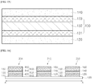
- FIG. 2 is a cross-sectional view of a magnetic sensor using an anomalous Hall effect according to a first embodiment of the present invention.
- a substrate 100 a buffer layer 110, a lower nonmagnetic metal layer 120, a ferromagnetic layer 130, and an upper nonmagnetic metal layer 140 are provided.
- the substrate 100 may be made of an insulating material and may include silicon oxide or silicon nitride. In addition, the substrate 100 may use any material as long as physical properties of the material are not significantly changed even when the buffer layer 110 to the upper nonmagnetic metal layer 140 are formed in subsequent processes.
- the buffer layer 110 is formed on the substrate 100.
- the buffer layer 110 is provided to facilitate the formation of the lower nonmagnetic metal layer 120. That is, when the lower nonmagnetic metal layer 120 is formed directly on the substrate 100 made of an insulating material, the lower nonmagnetic metal layer 120 may not have a predetermined lattice constant or may not form crystal grains, and thus, a polycrystalline structure may not be formed. Therefore, the lower nonmagnetic metal layer 120 is easily formed in a polycrystalline state through the formation of the buffer layer 110.
- the buffer layer 110 may be made of tantalum (Ta), rubidium (Ru), or titanium (Ti).
- the lower nonmagnetic metal layer 120 is formed on the buffer layer 110.
- the lower nonmagnetic metal layer 120 is in a polycrystalline state and causes stress at an interface with the ferromagnetic layer 130.
- the lower nonmagnetic metal layer 120 induces vertical magnetic anisotropy at an interface portion of the ferromagnetic layer 130 through magnetic interaction at the interface with the ferromagnetic layer 130.
- the lower nonmagnetic metal layer 120 may be made of platinum (Pt) or palladium (Pd).
- the ferromagnetic layer 130 is formed on the lower nonmagnetic metal layer 120.
- the ferromagnetic layer 130 is made of an alloy of CoFeSiB.
- Vertical magnetic anisotropy and horizontal magnetic anisotropy are mixed in a bulk region in the ferromagnetic layer 130. That is, vertical magnetization and horizontal magnetization are mixed, and middle magnetization between vertical magnetization and horizontal magnetization also appears.
- a lower region and an upper region of the ferromagnetic layer 130 are adjacent to or in contact with the nonmagnetic metal layers 120 and 140, and vertical magnetic anisotropy predominantly appears in the vicinity of a region in contact with the nonmagnetic metal layers 120 and 140.
- the vertical magnetization Due to the spin orbit interaction, in the ferromagnetic layer 130, the vertical magnetization is set as a magnetic easy axis. Therefore, when a magnetic field is applied in a direction perpendicular to the ferromagnetic layer 130, since a vertical direction becomes a magnetic easy axis, vertical magnetic anisotropy is enhanced in proportion to intensity of the magnetic field applied to the ferromagnetic layer 130, which appears as a Hall voltage.
- the upper nonmagnetic metal layer 140 is formed on the ferromagnetic layer 130.
- the upper nonmagnetic metal layer 140 may be made of Pt or Pd.
- the upper nonmagnetic metal layer 140 induces vertical magnetic anisotropy at the interface of the ferromagnetic layer 130 thereunder.
- a magnetic easy axis of the ferromagnetic layer 130 is determined in a vertical direction by the induced vertical magnetic anisotropy.
- the upper nonmagnetic metal layer 140 may be made of the same material as the lower nonmagnetic metal layer 120 so as to secure magnetic symmetry.
- the thickness of the upper nonmagnetic metal layer 140 may be the same as the thickness of the lower nonmagnetic metal layer 120.
- the magnetic symmetry may be secured, magnetic easy axes in the bulk region of the ferromagnetic layer 130 may be symmetrically set, and an offset of a Hall voltage, which is an output voltage of a Hall sensor to be manufactured, may be minimized.
- FIG. 3 is a detailed cross-sectional view of the magnetic sensor using the anomalous Hall effect of FIG. 2 according to the first embodiment of the present invention.
- the substrate and the buffer layer are omitted for convenience of description.
- the ferromagnetic layer 130 is provided between the lower nonmagnetic metal layer 120 and the upper nonmagnetic metal layer 140.
- a first easy axis induction layer 131 having enhanced vertical magnetic anisotropy is formed in a certain region from the interface of the ferromagnetic layer 130 in contact with the lower nonmagnetic metal layer 120, and a second easy axis induction layer 133 is formed in a certain region of the ferromagnetic layer 130 in contact with the upper nonmagnetic metal layer 140.
- the two easy axis induction layers 131 and 133 are formed due to interaction the ferromagnetic layer 130 at the interfaces with the nonmagnetic metal layers 120 and 140.
- the first easy axis induction layer 131 and the second easy axis induction layer 133 are made of the same material as a bulk layer 132 and are described as separate layers in terms of vertical magnetic anisotropy.
- the first easy axis induction layer 131 and the second easy axis induction layer 133 are characterized in that vertical magnetic anisotropy is predominant, and the bulk layer 132 between the easy axis induction layers 131 and 133 is characterized in that isotropy of a magnetization direction is predominant.
- a magnitude of vertical magnetic anisotropy induced in the bulk layer 132 of the ferromagnetic layer 130 may be proportional to intensity of an applied magnetic field, and thus, it is possible to secure linearity of a Hall voltage which is an output voltage.
- a magnetic sensor is manufactured using a direct current (DC) magnetron sputter.
- Deposition pressure in a chamber is set to be in a range from 3 mTorr to 5 mTorr.
- each target is disposed, and gun power is used.
- a substrate is made of SiO 2
- a buffer layer is made of Ta
- a lower nonmagnetic metal layer is made of Pt
- a ferromagnetic layer is made of CoFeSiB
- an upper nonmagnetic metal layer is made of the same Pt as the lower nonmagnetic metal layer.
- Gun power applied to a Ta target is 60 W
- gun power applied to a Pt target is 60 W
- gun power applied to a CoFeSiB target is 80 W.
- a thickness of Ta constituting the buffer layer deposited on the SiO 2 substrate is 50 ⁇
- a thickness of Pt constituting the lower nonmagnetic metal layer is 25 ⁇
- a thickness of Pt constituting the upper nonmagnetic metal layer is 25 ⁇ .
- the samples are divided according to the thickness of the ferromagnetic layer. The samples are classified in Table 1 below.
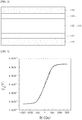
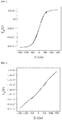
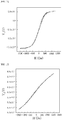
- FIGS. 4 to 6 are graphs showing a linear property of an output voltage according to a change in thickness of the ferromagnetic layer according to Manufacturing Example 1 of the present invention.
- the samples have a square shape, a current is applied to a surface of the upper nonmagnetic metal layer which is a top layer, and a magnetic field is applied in a direction perpendicular to a surface of the substrate.
- a Hall voltage is measured in a direction perpendicular to a direction of the applied current and to a direction of the applied magnetic field. That is, when a current is applied to facing sides of a square shape of the upper nonmagnetic metal layer, the Hall voltage is measured at sides perpendicular to the facing sides.
- a measurement method of the Hall voltage is equally applied to other Manufacturing Examples below.
- FIG. 4 shows a linear property of a Hall voltage which is an output voltage when a thickness of CoFeSiB is 25 ⁇ .
- the Hall voltage shows an excellent linear property between about 4 mV and about 4.8 mV.
- FIG. 5 shows a linear property of a Hall voltage which is an output voltage when a thickness of CoFeSiB is 35 ⁇ .
- the Hall voltage shows an excellent linear property between about -0.6 mV and about 0.2 mV.
- the difference value between the Hall voltages is a value of 0.8 mV and the Hall voltages have an excellent linear property when the thickness of CoFeSiB is less than or equal to 35 ⁇ .
- the thickness of CoFeSiB was reduced to 10 ⁇ in another manufactured sample, the same linear property could be obtained.
- a linear property with respect to a thickness less than 10 ⁇ is not confirmed due to a limitation of manufacturing equipment.
- FIG. 6 shows a linear property of a Hall voltage which is an output voltage when a thickness of CoFeSiB is 55 ⁇ .
- a nonlinear property appears with respect to a magnetic field intensity of zero oersteds (Oe), and there is no saturation magnetization that should be required in a Hall sensor. Therefore, a specific range in which an applied magnetic field may be sensed is not determined, and due to the nonlinear property, the Hall sensor is not considered to be used as a magnetic sensor.
- a matter confirmable in the present Manufacturing Example is that there is a certain limitation on the thickness of the ferromagnetic layer. That is, when the thickness of the ferromagnetic layer reaches 55 ⁇ , it can be seen that vertical magnetic anisotropy of the ferromagnetic layer is damaged due to the increased thickness. Even when vertical magnetic anisotropy appears in an interface region due to the nonmagnetic metal layers disposed on and below the ferromagnetic layer, it can be confirmed that the thickness of the bulk layer is also increased due to the increased thickness and a magnetic easy axis is difficult to form.
- the thickness of the ferromagnetic layer may be in a range of 10 ⁇ to 45 ⁇ .
- the thickness of the ferromagnetic layer needs to be greater than or equal to the thickness of the upper nonmagnetic metal layer or the lower nonmagnetic metal layer. This is related to an amount of a current flowing in the ferromagnetic layer.
- a current needs to flow in the ferromagnetic layer in an amount greater than or equal to a certain ratio with respect to an amount of a current flowing to the nonmagnetic metal layer.
- the amount of the current flowing in the ferromagnetic layer may not be detected due to a limitation of measurement.
- the thickness of the ferromagnetic layer needs to have a value greater than or equal to the thickness of each of the nonmagnetic metal layers.
- a magnetic sensor is manufactured using a DC magnetron sputter. Pressure in a chamber and gun power with respect to a target for manufacturing the magnetic sensor are the same as those described in Manufacturing Example 1 above. However, thicknesses of a lower nonmagnetic metal layer, a ferromagnetic layer, and an upper nonmagnetic metal layer are fixed and a thickness of a buffer layer is changed, thereby manufacturing three samples. The manufactured samples classified according to the thickness of the buffer layer are shown in Table 2.
- FIGS. 7 to 9 are graphs showing a linear property of an output voltage according to a change in thickness of the buffer layer according to Manufacturing Example 2 of the present invention.
- FIG. 7 shows a linear property of a Hall voltage which is an output voltage when a thickness of Ta constituting a buffer layer is 30 ⁇
- FIG. 8 shows a linear property of a Hall voltage which is an output voltage when a thickness of Ta constituting a buffer layer is 50 ⁇
- the thickness of the buffer layer may be less than or equal to 50 ⁇ .
- a thickness of Ta is 70 ⁇
- linearity of a magnetic sensor is weakened, and responsiveness of a Hall voltage with respect to intensity of an applied magnetic field is lowered.
- the thickness of the buffer layer is greater than or equal to a certain thickness, it can be seen that resolution of the magnetic sensor is reduced and sensitivity thereof is very weak.
- saturation of magnetization completely disappears, the magnetic sensor may not be used as a magnetic sensor.
- a magnetic sensor is manufactured using a DC magnetron sputter. Pressure in a chamber and gun power with respect to a target for manufacturing the magnetic sensor are the same as those described in Manufacturing Example 1 above. However, thicknesses of a buffer layer, a ferromagnetic layer, and an upper nonmagnetic metal layer are fixed and a thickness of a lower nonmagnetic metal layer is changed, thereby manufacturing three samples. The manufactured samples classified according to the thickness of the lower nonmagnetic metal layer are shown in Table 3.
- FIGS. 10 to 12 are graphs showing a linear property of an output voltage according to a change in thickness of the lower nonmagnetic metal layer according to Manufacturing Example 3 of the present invention.
- FIG. 10 shows a linear property of a Hall voltage which is an output voltage when a thickness of Pt constituting a lower nonmagnetic metal layer is 15 ⁇ .
- FIG. 11 shows a linear property of a Hall voltage which is an output voltage when a thickness of Pt constituting a lower nonmagnetic metal layer is 35 ⁇ .
- FIG. 12 shows a linear property of a Hall voltage which is an output voltage when a thickness of Pt constituting a lower nonmagnetic metal layer is 45 ⁇ .
- the thickness of the lower nonmagnetic metal layer is less than or equal to the thickness of the ferromagnetic layer, it can be seen that a Hall voltage shows a linear property and a voltage difference between the Hall voltages is also the same in a linear trajectory before a saturation magnetization state.
- the Hall voltage is abruptly changed even in a low magnetic field. This means that, as the thickness of the lower nonmagnetic metal layer is reduced, sensing sensitivity is improved.
- the thickness of the lower nonmagnetic metal layer is reduced, stress of a structure of the lower nonmagnetic metal layer greatly acts on an interface of a ferromagnetic material, thereby enhancing vertical magnetic anisotropy of the ferromagnetic material. That is, as the thickness of the lower nonmagnetic metal layer is reduced, the stress of the lower nonmagnetic metal layer is increased, which acts on an interface of a ferromagnetic material to enhance vertical magnetic anisotropy of a first easy axis induction layer of the ferromagnetic layer. Therefore, a magnetic easy axis is increased in a bulk layer of the ferromagnetic layer, and a Hall voltage reacts sensitively according to intensity of an applied magnetic field, thereby improving sensitivity and improving linearity.
- the thickness of the lower nonmagnetic metal layer is set to be less than or equal to the thickness of the ferromagnetic layer
- a current flows in the ferromagnetic layer in an amount greater than or equal to a certain ratio with respect to an amount of a current flowing to the lower nonmagnetic metal layer.
- An anomalous Hall effect is generated by the current flowing in the ferromagnetic layer, and linearity is improved by the anomalous Hall effect.
- a conventional Hall effect and an anomalous Hall effect concurrently appear in the ferromagnetic layer.
- a Hall voltage is generated in proportion to an applied magnetic field.
- the ferromagnetic layer is made of a metal material, even when a current is supplied thereto, due to lattice scattering of electrons, the conventional Hall effect is not greater than that of the semiconductor. Therefore, when a thickness of the ferromagnetic material is set to be greater than or equal to the thickness of the lower nonmagnetic metal layer, contribution of the Hall voltage by the conventional Hall effect is reduced or insignificant. However, the contribution of the Hall voltage by the anomalous Hall effect is increased.
- the nonmagnetic metal layers are disposed on and below the ferromagnetic material, and the two nonmagnetic metal layers include the same material.
- the thickness of the ferromagnetic material is set to be less than or equal to 45 ⁇ or less. When the thickness exceeds 45 ⁇ , a magnetic easy axis in a vertical direction in the ferromagnetic material may be difficult to form, and vertical magnetic anisotropy may not be secured. Therefore, even when a magnetic field and an input current are increased, a sensitivity characteristic may not be secured, and linearity may be destroyed.
- the thickness of the nonmagnetic metal layer in contact with the ferromagnetic material is set to be less than or equal to the thickness of the ferromagnetic material. Therefore, a magnetic sensor with excellent linearity and high sensitivity may be obtained.
- FIG. 13 is a plan view of a Hall sensor using an anomalous Hall effect according to a second embodiment of the present invention.
- the Hall sensor includes a sensing region 210, an electrode line portion 220, and a pad portion 230.
- the sensing region 210, the electrode line portion 220, and the pad portion 230 are formed on a substrate 100.
- the substrate 100 may be made of an insulating material and may include SiO 2 or SiN.
- the substrate 100 may use any material as long as physical properties of the material are not significantly changed even when subsequent processes are performed.
- the sensing region 210 has an approximately rhombic shape, and vertices of a rhombus are connected to the electrode line portion 220.
- a Hall voltage is generated by an applied magnetic field. That is, a Hall voltage according to an anomalous Hall effect is generated in the sensing region 210.
- the sensing region 210 having the rhombic shape, a Hall voltage is generated according to a change in vertical magnetic anisotropy.
- the sensing region 210 has a rhombic shape in order to secure linearity and increase a level of the generated Hall voltage.
- a first electrode line 221 and a third electrode line 223 are formed in a y direction which is parallel to a long axis of the rhombus.
- a second electrode line 222 and a fourth electrode line 224 are formed in an x direction which is parallel to a short axis of a rhombus.
- a width in the y direction parallel to the long axis may be 1 time or 1.5 times a width in the x direction parallel to the short axis.
- two electrode lines 221 and 223 in the y direction are used to sense a Hall voltage.
- a magnetic field is applied in a direction perpendicular to a surface of the sensing region 210.
- the sensing region 210 having the rhombic shape of the present invention may use all magnetic fields applied to the rhombus to generate a Hall voltage.
- the input current is applied in the x direction parallel to the short axis and the Hall voltage is output at two vertices in the y direction parallel to the long axis, but vice versa.
- the electrode line portion 220 is integrally formed with the pad portion 230 and includes four pads 231, 232, 233, and 234.
- FIG. 14 is a cross-sectional view taken along line A-A' of the Hall sensor of FIG. 13 according to the second embodiment of the present invention.
- a fourth pad 234, the sensing region 210, and a second pad 232 are shown on the substrate 100.
- the fourth pad 234, the sensing region 210, and the second pad 232 have the same stacked structure, and the same applies to other pads and the electrode line portion not shown in FIG. 14 . That is, a stacked structure of the electrode line portion 220 and the pad portion 230 is the same as that of the sensing region 210.
- the fourth pad 234 includes a buffer layer 110, a lower nonmagnetic metal layer 120, a ferromagnetic layer 130, and an upper nonmagnetic metal layer 140 on the substrate 100, and the same applies to the sensing region 210 and the second pad 232.
- the buffer layer 110 is formed on the substrate 100.
- the buffer layer 110 is provided to facilitate the formation of the lower nonmagnetic metal layer 120. That is, when the lower nonmagnetic metal layer 120 is formed directly on the substrate 100 made of the insulating material, the lower nonmagnetic metal layer 120 may not have a predetermined lattice constant or may not form crystal grains, and thus, a polycrystalline structure may not be formed. Therefore, the lower nonmagnetic metal layer 120 is easily formed in a polycrystalline state through the formation of the buffer layer 110.
- the buffer layer 110 may be made of Ta, Ru, or Ti.
- the lower nonmagnetic metal layer 120 is formed on the buffer layer 110.
- the lower nonmagnetic metal layer 120 is in a polycrystalline state and causes stress at an interface with the ferromagnetic layer 130.
- the lower nonmagnetic metal layer 120 induces vertical magnetic anisotropy at an interface portion of the ferromagnetic layer 130 through magnetic interaction at the interface with the ferromagnetic layer 130.
- the lower nonmagnetic metal layer 120 may be made of Pt or Pd.
- the ferromagnetic layer 130 is formed on the lower nonmagnetic metal layer 120.
- the ferromagnetic layer 130 is made of an alloy of CoFeSiB.
- Vertical magnetic anisotropy and horizontal magnetic anisotropy are mixed in a bulk region in the ferromagnetic layer 130. That is, vertical magnetization and horizontal magnetization are mixed, and magnetization in a middle region between vertical magnetization and horizontal magnetization also appears.
- a lower region and an upper region of the ferromagnetic layer 130 are adjacent to or in contact with the nonmagnetic metal layers 120 and 140, and vertical magnetic anisotropy dominantly appears in the vicinity of a region in contact with the nonmagnetic metal layers 120 and 140.
- the upper nonmagnetic metal layer 140 is formed on the ferromagnetic layer 130.
- the upper nonmagnetic metal layer 140 may be made of Pt or Pd.
- the upper nonmagnetic metal layer 140 induces vertical magnetic anisotropy at the interface of the lower ferromagnetic layer 130.
- the magnetic easy axis of the ferromagnetic layer 130 is determined in a vertical direction by the induced vertical magnetic anisotropy.
- the upper nonmagnetic metal layer 140 may be made of the same material as the lower nonmagnetic metal layer 120 so as to secure magnetic symmetry.
- the thickness of the upper nonmagnetic metal layer 140 may be the same as the thickness of the lower nonmagnetic metal layer 120.
- the magnetic symmetry may be secured, easy magnetization axes in the bulk region of the ferromagnetic layer 130 may be symmetrically set, and an offset of a Hall voltage, which is an output voltage of a Hall sensor to be manufactured, may be minimized.
- an input current is first supplied to the upper nonmagnetic metal layer 140 through the pads. Since the upper nonmagnetic metal layer 140, the ferromagnetic layer 130, and the lower nonmagnetic metal layer 120 are made of a metal material, an input current is diffused and flows in compliance with each resistance. Furthermore, two remaining pads corresponding to the pads determined as input terminals form output terminals. The Hall voltage, which is output, is output through the upper nonmagnetic metal layer 140.
- FIG. 15 is a detailed cross-sectional view for describing operations of the sensing region of the Hall sensor of FIG. 13 according to the second embodiment of the present invention.
- the substrate and the buffer layer are omitted for convenience of description.
- the ferromagnetic layer 130 is provided between the lower nonmagnetic metal layer 120 and the upper nonmagnetic metal layer 140.
- a first easy axis induction layer 131 having enhanced vertical magnetic anisotropy is formed in a certain region from the interface of the ferromagnetic layer 130 in contact with the lower nonmagnetic metal layer 120, and a second easy axis induction layer 133 is formed in a certain region of the layer 130 in contact with the upper nonmagnetic metal layer 140.
- the two easy axis induction layers 131 and 133 are formed due to interaction at the interfaces with the nonmagnetic metal layers 120 and 140.
- the first easy axis induction layer 131 and the second easy axis induction layer 133 are made of the same material as a bulk layer 132 and are described as separate layers in terms of vertical magnetic anisotropy.
- the first easy axis induction layer 131 and the second easy axis induction layer 133 are characterized in that vertical magnetic anisotropy is predominant, and the bulk layer 132 between the easy axis induction layers 131 and 133 is characterized in that isotropy of a magnetization direction is predominant.
- a magnitude of vertical magnetic anisotropy induced in the bulk layer 132 of the ferromagnetic layer 130 may be proportional to intensity of an applied magnetic field, and thus, it is possible to secure linearity of a Hall voltage which is an output voltage.
- the Hall voltage is data that is measurable only when all output nodes for measuring a magnetic field applied perpendicular to a surface of the ferromagnetic layer, an input current, and a Hall voltage are provided in one element. That is, the electrode line portion lacks any one of the input current and the output node, and the pad portion also lacks any one of the input current and the output node, and thus, the electrode line portion and the pad portion do not affect a Hall voltage generated in the sensing region.
- FIG. 16 is another cross-sectional view taken along line A-A' of the Hall sensor of FIG. 13 according to the second embodiment of the present invention.
- the fourth pad 234, the sensing region 210, and the second pad 232 are formed on the substrate 100.
- the fourth pad 234, the sensing region 210, and the second pad 232 have the same stacked structure.
- the stacked structure is a structure in which a ferromagnetic layer and a nonmagnetic metal layer are added to the stacked structure shown in FIG. 14 .
- the buffer layer 110 a lower nonmagnetic metal layer 120, a ferromagnetic layer 130, an upper nonmagnetic metal layer 140, an additional ferromagnetic layer 150, and an additional nonmagnetic metal layer 160 are formed on the substrate 100.
- the material of the buffer layer 110 is the same as that described with reference to FIG. 14 . Therefore, the buffer layer 110 may be made of Ta, Ru, or Ti. In addition, the material of the nonmagnetic metal layers 120, 140, and 160 includes Pt or Pd as described above with reference to FIG. 14 . In addition, the material of the ferromagnetic layers 130 and 150 includes CoFeSiB. That is, FIG. 16 shows a structure in which the nonmagnetic metal layers 120, 140, and 160 are arranged on and below the ferromagnetic layers 130 and 150 and the arrangement is repeated.
- the additional ferromagnetic layer 150 has a structure which shares one nonmagnetic metal layer 140, which is interposed between the additional ferromagnetic layer 150 and the lower ferromagnetic layer 130 thereunder, with the lower ferromagnetic layer 130.
- a thickness of each buffer layer 110 may be in a range of 10 ⁇ to 50 ⁇ .
- the thickness of the buffer layer 110 exceeds 50 ⁇ , it can be seen that linearity of a Hall voltage is weakened and sensing sensitivity is lowered. This means that vertical magnetic anisotropy does not smoothly act in the ferromagnetic layer.
- stress generated between the buffer layer 110 and the lower nonmagnetic metal layer 120 is absorbed due to the large thickness of the buffer layer 110. Therefore, stress applied to the ferromagnetic layer 130 in the form of energy is also reduced at an interface of the lower nonmagnetic metal layer 120 in contact with the ferromagnetic layer 130. As a result, intensity of vertical magnetization is reduced, and thus, vertical magnetic anisotropy is weakened.
- each of the ferromagnetic layers 130 and 150 may be in a range of 10 ⁇ to 45 ⁇ . It is difficult to manufacture the ferromagnetic layers 130 and 150 including a CoFeSiB material to have a thickness less than 10 ⁇ . In addition, when the thickness of the ferromagnetic layers 130 and 150 exceeds 45 ⁇ , it is confirmed that linearity is degraded, a curve related to saturation magnetization disappears, and very low sensitivity is obtained with respect to an applied magnetic field.
- each of the nonmagnetic metal layers 120, 140, and 160 may be less than or equal to the thickness of the ferromagnetic layers 130 and 150.
- manufacturing the nonmagnetic metal layers 120, 140, and 160 to have a thickness less than 10 ⁇ is very difficult in view of a process. Therefore, the thickness of the nonmagnetic metal layers 120, 140, and 160 needs to be greater than or equal to 10 ⁇ and less than or equal to the thickness of the ferromagnetic layers 130 and 150.
- the thickness of the nonmagnetic metal layers 120, 140, and 160 is less than or equal to the thickness of the ferromagnetic layers 130 and 150, it can be seen that a Hall voltage shows a linear property, and a voltage difference is also the same in a linear trajectory before a saturation magnetization state.
- a Hall voltage tends to be abruptly changed even in a low magnetic field. This means that, as the thickness of the nonmagnetic metal layers 120, 140, and 160 is reduced, sensing sensitivity is improved.
- the thickness of the nonmagnetic metal layers 120, 140, and 160 exceeds the thickness of the ferromagnetic layers 130 and 150, linearity is degraded, and saturation magnetization is not generated. Sensitivity is also abruptly lowered. This means that, when a current flowing in the nonmagnetic metal layers 120, 140, and 160 exceeds a current flowing in the ferromagnetic layers 130 and 15 and a current is concentrated in the nonmagnetic metal layers 120, 140, and 160 at a certain ratio or more, it is difficult to remove magnetic anisotropy.
- the nonmagnetic metal layers 120, 140, and 160 having increased thickness may not cause energy or stress at interfaces with the ferromagnetic layers 130 and 150 including thick bulk regions therein. Therefore, it is difficult to generate a magnetic easy axis according to vertical magnetic anisotropy.
- FIGS. 17 and 18 show plan views and cross-sectional views illustrating a method of manufacturing the Hall sensor of FIGS. 13 and 14 according to the second embodiment of the present invention.
- the buffer layer 110, the lower nonmagnetic metal layer 120, the ferromagnetic layer 130, and the upper nonmagnetic metal layer 140 are sequentially formed on the substrate 100 through various methods including sputtering.
- the thickness and material of each layer are the same as those described above.
- the layers are formed on an entire surface of the substrate 100, and the upper nonmagnetic metal layer 140 is exposed at a top layer.
- a photoresist pattern 118 is formed on the upper nonmagnetic metal layer 140 of the top layer.
- the photoresist pattern 118 is formed according to a known photolithography process. That is, a photoresist is applied on the upper nonmagnetic metal layer 140, and the photoresist pattern 118 is formed through a typical photolithography process.
- etching is performed using the formed photoresist pattern 118 as an etching mask such that a portion of the substrate 100 below the photoresist pattern 118 is exposed.
- a Hall sensor pattern shape shown in FIGS. 13 and 14 may be obtained.
- the photoresist pattern 118 on the substrate 100 is removed using a process including ashing, and a surface of the upper nonmagnetic metal layer 140 of the top layer is exposed.
- the sensing region 210 of the present embodiment has the same stacked structure as the electrode line portion 220.
- the sensing region 210 also has the same stacked structure as the pad portion 230. That is, separate metal layer forming and patterning processes for forming an electrode line are not required. The same applies to the pad portion.
- the sensing region, the electrode line portion, and the pad portion are concurrently formed by performing forming and etching processes of a photoresist pattern only once. Therefore, complicated processes may be omitted in a production process, and productivity may be improved.
- a Hall sensor is manufactured using a DC magnetron sputter. Deposition pressure in a chamber is set to a range of 3 mTorr to 5 mTorr. In order for deposition to occur, each target is disposed, and gun power was used.
- a substrate is made of SiO 2 , a buffer layer is made of Ta, a lower nonmagnetic metal layer is made of Pt, a ferromagnetic layer is made of CoFeSiB, and an upper nonmagnetic metal layer is made of the same Pt as the lower nonmagnetic metal layer.
- Gun power applied to a Ta target is 60 W
- gun power applied to a Pt target is 60 W
- gun power applied to a CoFeSiB target is 80 W.
- a thickness of Ta constituting the buffer layer deposited on the SiO 2 substrate is 50 ⁇
- a thickness of Pt constituting the lower nonmagnetic metal layer is 25 ⁇
- a thickness of Pt constituting the upper nonmagnetic metal layer is 25 ⁇
- a thickness of CoFeSiB constituting the ferromagnetic layer is 35 ⁇ .
- input resistance is divided into four values by changing a line width of the electrode line portion.
- input lines are set to face each other, and output lines are set to face each other.
- a line width is adjusted to set output resistance to 1.3 k ⁇ .
- the samples divided according to a change in input resistance are classified in Table 4 below. [Table 4] Classification Input line width Input resistance Output line width Output resistance Sample 1 25 ⁇ m 1.6 k ⁇ 50 ⁇ m 1.3 k ⁇ Sample 2 50 ⁇ m 1.2 k ⁇ Sample 3 75 ⁇ m 890 ⁇ Sample 4 100 ⁇ m 550 ⁇
- FIGS. 19 to 22 are graphs showing a change in Hall voltage according to application of a magnetic field according to Manufacturing Example 4 of the present invention.
- FIG. 19 shows a change in Hall voltage when input resistance is 1.6 kQ
- FIG. 20 shows a change in Hall voltage when input resistance is 1.2 kQ
- FIG. 21 shows a change in Hall voltage when input resistance is 890 ⁇
- FIG. 22 shows a change in Hall voltage when input resistance is 550 ⁇ .
- a width ratio of a long axis to a short axis is 1.5, an input current is applied to the short axis, and a Hall voltage is measured at a vertex of the long axis.
- the Hall voltage is performed by probing the upper nonmagnetic metal layer exposed at the pad portion.
- an absolute value of a difference between a Hall voltage when intensity of an applied magnetic field has a negative value and saturation magnetization is formed and a Hall voltage when a magnetic field has a positive value and saturation magnetization is formed is a value of about 14 ⁇ 10 -4 V. That is, even when a value of input resistance is changed, it can be seen that characteristics of the Hall voltage are hardly changed. Therefore, even when a width of an electrode line for input is slightly changed, Hall sensors having the same characteristics may be obtained. In a Hall sensor, a change in Hall voltage also needs to be sensitive when intensity of an applied magnetic field is changed. Thus, improved sensitivity may be obtained.
- the electrode line portion and the pad portion have the same stacked structure as the sensing region, a connection of each element is in a physically continuous state and the element is formed by patterning one stacked structure.
- any one of an input current and an output node is in a lacking state, thereby forming a stable Hall voltage.
- the electrode line portion and the pad portion have the same stacked structure as the sensing region. That is, in a manufacturing process, one photo mask may be used, and an etching process may be performed once, thereby manufacturing a Hall sensor. Thus, high productivity is secured.
- a magnetic field applied in a direction perpendicular to an interface is used, and an anomalous Hall effect is used in which intensity of vertical magnetic anisotropy of a ferromagnetic layer is changed according to the applied magnetic field. Therefore, it is possible to obtain a Hall sensor which is insensitive to a change in temperature change and has high sensitivity, and it is possible to induce a Hall effect by applying a magnetic field in a direction perpendicular to an interface of the ferromagnetic layer, thereby applying the Hall sensor in a very flexible use environment.
Landscapes
- Physics & Mathematics (AREA)
- Condensed Matter Physics & Semiconductors (AREA)
- General Physics & Mathematics (AREA)
- Hall/Mr Elements (AREA)
- Measuring Magnetic Variables (AREA)
Applications Claiming Priority (3)
| Application Number | Priority Date | Filing Date | Title |
|---|---|---|---|
| KR1020180152366A KR102609451B1 (ko) | 2018-11-30 | 2018-11-30 | 금속 다층 박막을 가지는 이상 홀 효과 자기 센서 |
| KR1020180152367A KR102633304B1 (ko) | 2018-11-30 | 2018-11-30 | 이상 홀 효과를 이용하는 홀 센서 및 이의 제조방법 |
| PCT/KR2019/016704 WO2020111862A1 (ko) | 2018-11-30 | 2019-11-29 | 이상 홀 효과를 이용하는 자기 센서, 홀 센서 및 홀 센서의 제조방법 |
Publications (2)
| Publication Number | Publication Date |
|---|---|
| EP3889628A1 true EP3889628A1 (de) | 2021-10-06 |
| EP3889628A4 EP3889628A4 (de) | 2022-01-12 |
Family
ID=
Also Published As
| Publication number | Publication date |
|---|---|
| US11815569B2 (en) | 2023-11-14 |
| US20220026506A1 (en) | 2022-01-27 |
| JP7207671B2 (ja) | 2023-01-18 |
| CN113167841A (zh) | 2021-07-23 |
| CN113167841B (zh) | 2024-08-20 |
| JP2022510249A (ja) | 2022-01-26 |
| WO2020111862A1 (ko) | 2020-06-04 |
Similar Documents
| Publication | Publication Date | Title |
|---|---|---|
| US11815569B2 (en) | Magnetic sensor and hall sensor, each using anomalous hall effect, and method for manufacturing hall sensor | |
| CN102565727B (zh) | 用于测量磁场的磁电阻传感器 | |
| US7872564B2 (en) | Integrated lateral short circuit for a beneficial modification of current distribution structure for xMR magnetoresistive sensors | |
| US6577124B2 (en) | Magnetic field sensor with perpendicular axis sensitivity, comprising a giant magnetoresistance material or a spin tunnel junction | |
| US7483295B2 (en) | MTJ sensor including domain stable free layer | |
| US7355822B2 (en) | Superparamagnetic field sensing device | |
| JP6193212B2 (ja) | シングルチップ2軸ブリッジ型磁界センサ | |
| US6771472B1 (en) | Structure to achieve thermally stable high sensitivity and linear range in bridge GMR sensor using SAF magnetic alignments | |
| US11467232B2 (en) | Magnetoresistive sensor and fabrication method for a magnetoresistive sensor | |
| US20200033424A1 (en) | Magnetoresistance Assembly Having a TMR Element Disposed Over or Under a GMR Element | |
| CN102621504A (zh) | 单片参考全桥磁场传感器 | |
| US10263179B2 (en) | Method of forming tunnel magnetoresistance (TMR) elements and TMR sensor element | |
| WO2000041250A1 (en) | Spin dependent tunneling sensor | |
| US11209505B2 (en) | Large field range TMR sensor using free layer exchange pinning | |
| WO2021040801A1 (en) | Tmr sensor with magnetic tunnel junctions with a free layer having an intrinsic anisotropy | |
| Sun et al. | Tunneling magnetoresistance and current distribution effect in spin-dependent tunnel junctions | |
| CN202494772U (zh) | 用于测量磁场的磁电阻传感器 | |
| KR102633304B1 (ko) | 이상 홀 효과를 이용하는 홀 센서 및 이의 제조방법 |
Legal Events
| Date | Code | Title | Description |
|---|---|---|---|
| STAA | Information on the status of an ep patent application or granted ep patent |
Free format text: STATUS: THE INTERNATIONAL PUBLICATION HAS BEEN MADE |
|
| PUAI | Public reference made under article 153(3) epc to a published international application that has entered the european phase |
Free format text: ORIGINAL CODE: 0009012 |
|
| STAA | Information on the status of an ep patent application or granted ep patent |
Free format text: STATUS: REQUEST FOR EXAMINATION WAS MADE |
|
| 17P | Request for examination filed |
Effective date: 20210607 |
|
| AK | Designated contracting states |
Kind code of ref document: A1 Designated state(s): AL AT BE BG CH CY CZ DE DK EE ES FI FR GB GR HR HU IE IS IT LI LT LU LV MC MK MT NL NO PL PT RO RS SE SI SK SM TR |
|
| A4 | Supplementary search report drawn up and despatched |
Effective date: 20211214 |
|
| RIC1 | Information provided on ipc code assigned before grant |
Ipc: H01L 43/10 20060101ALI20211208BHEP Ipc: H01L 43/06 20060101ALI20211208BHEP Ipc: G01R 33/00 20060101ALI20211208BHEP Ipc: G01R 33/07 20060101AFI20211208BHEP |
|
| DAV | Request for validation of the european patent (deleted) | ||
| DAX | Request for extension of the european patent (deleted) | ||
| P01 | Opt-out of the competence of the unified patent court (upc) registered |
Effective date: 20230518 |
|
| STAA | Information on the status of an ep patent application or granted ep patent |
Free format text: STATUS: EXAMINATION IS IN PROGRESS |
|
| 17Q | First examination report despatched |
Effective date: 20250103 |