EP3893280A1 - Dispositif d'affichage utilisant des éléments électroluminescents à semi-conducteur et son procédé de fabrication - Google Patents
Dispositif d'affichage utilisant des éléments électroluminescents à semi-conducteur et son procédé de fabrication Download PDFInfo
- Publication number
- EP3893280A1 EP3893280A1 EP19893669.2A EP19893669A EP3893280A1 EP 3893280 A1 EP3893280 A1 EP 3893280A1 EP 19893669 A EP19893669 A EP 19893669A EP 3893280 A1 EP3893280 A1 EP 3893280A1
- Authority
- EP
- European Patent Office
- Prior art keywords
- layer
- semiconductor light
- emitting element
- display device
- light
- Prior art date
- Legal status (The legal status is an assumption and is not a legal conclusion. Google has not performed a legal analysis and makes no representation as to the accuracy of the status listed.)
- Granted
Links
Images



Classifications
-
- H—ELECTRICITY
- H10—SEMICONDUCTOR DEVICES; ELECTRIC SOLID-STATE DEVICES NOT OTHERWISE PROVIDED FOR
- H10H—INORGANIC LIGHT-EMITTING SEMICONDUCTOR DEVICES HAVING POTENTIAL BARRIERS
- H10H20/00—Individual inorganic light-emitting semiconductor devices having potential barriers, e.g. light-emitting diodes [LED]
- H10H20/01—Manufacture or treatment
- H10H20/011—Manufacture or treatment of bodies, e.g. forming semiconductor layers
- H10H20/018—Bonding of wafers
-
- H—ELECTRICITY
- H10—SEMICONDUCTOR DEVICES; ELECTRIC SOLID-STATE DEVICES NOT OTHERWISE PROVIDED FOR
- H10P—GENERIC PROCESSES OR APPARATUS FOR THE MANUFACTURE OR TREATMENT OF DEVICES COVERED BY CLASS H10
- H10P50/00—Etching of wafers, substrates or parts of devices
- H10P50/60—Wet etching
- H10P50/61—Electrolytic etching
- H10P50/617—Electrolytic etching of Group III-V materials
-
- H—ELECTRICITY
- H10—SEMICONDUCTOR DEVICES; ELECTRIC SOLID-STATE DEVICES NOT OTHERWISE PROVIDED FOR
- H10H—INORGANIC LIGHT-EMITTING SEMICONDUCTOR DEVICES HAVING POTENTIAL BARRIERS
- H10H20/00—Individual inorganic light-emitting semiconductor devices having potential barriers, e.g. light-emitting diodes [LED]
- H10H20/80—Constructional details
- H10H20/84—Coatings, e.g. passivation layers or antireflective coatings
-
- H—ELECTRICITY
- H10—SEMICONDUCTOR DEVICES; ELECTRIC SOLID-STATE DEVICES NOT OTHERWISE PROVIDED FOR
- H10H—INORGANIC LIGHT-EMITTING SEMICONDUCTOR DEVICES HAVING POTENTIAL BARRIERS
- H10H20/00—Individual inorganic light-emitting semiconductor devices having potential barriers, e.g. light-emitting diodes [LED]
- H10H20/80—Constructional details
- H10H20/85—Packages
- H10H20/851—Wavelength conversion means
-
- H—ELECTRICITY
- H10—SEMICONDUCTOR DEVICES; ELECTRIC SOLID-STATE DEVICES NOT OTHERWISE PROVIDED FOR
- H10H—INORGANIC LIGHT-EMITTING SEMICONDUCTOR DEVICES HAVING POTENTIAL BARRIERS
- H10H20/00—Individual inorganic light-emitting semiconductor devices having potential barriers, e.g. light-emitting diodes [LED]
- H10H20/80—Constructional details
- H10H20/85—Packages
- H10H20/857—Interconnections, e.g. lead-frames, bond wires or solder balls
-
- H—ELECTRICITY
- H10—SEMICONDUCTOR DEVICES; ELECTRIC SOLID-STATE DEVICES NOT OTHERWISE PROVIDED FOR
- H10H—INORGANIC LIGHT-EMITTING SEMICONDUCTOR DEVICES HAVING POTENTIAL BARRIERS
- H10H29/00—Integrated devices, or assemblies of multiple devices, comprising at least one light-emitting semiconductor element covered by group H10H20/00
- H10H29/01—Manufacture or treatment
- H10H29/03—Manufacture or treatment using mass transfer of LEDs, e.g. by using liquid suspensions
-
- H—ELECTRICITY
- H10—SEMICONDUCTOR DEVICES; ELECTRIC SOLID-STATE DEVICES NOT OTHERWISE PROVIDED FOR
- H10H—INORGANIC LIGHT-EMITTING SEMICONDUCTOR DEVICES HAVING POTENTIAL BARRIERS
- H10H29/00—Integrated devices, or assemblies of multiple devices, comprising at least one light-emitting semiconductor element covered by group H10H20/00
- H10H29/01—Manufacture or treatment
- H10H29/034—Manufacture or treatment of coatings
-
- H—ELECTRICITY
- H10—SEMICONDUCTOR DEVICES; ELECTRIC SOLID-STATE DEVICES NOT OTHERWISE PROVIDED FOR
- H10W—GENERIC PACKAGES, INTERCONNECTIONS, CONNECTORS OR OTHER CONSTRUCTIONAL DETAILS OF DEVICES COVERED BY CLASS H10
- H10W90/00—Package configurations
-
- H—ELECTRICITY
- H10—SEMICONDUCTOR DEVICES; ELECTRIC SOLID-STATE DEVICES NOT OTHERWISE PROVIDED FOR
- H10H—INORGANIC LIGHT-EMITTING SEMICONDUCTOR DEVICES HAVING POTENTIAL BARRIERS
- H10H20/00—Individual inorganic light-emitting semiconductor devices having potential barriers, e.g. light-emitting diodes [LED]
- H10H20/01—Manufacture or treatment
- H10H20/034—Manufacture or treatment of coatings
-
- H—ELECTRICITY
- H10—SEMICONDUCTOR DEVICES; ELECTRIC SOLID-STATE DEVICES NOT OTHERWISE PROVIDED FOR
- H10H—INORGANIC LIGHT-EMITTING SEMICONDUCTOR DEVICES HAVING POTENTIAL BARRIERS
- H10H20/00—Individual inorganic light-emitting semiconductor devices having potential barriers, e.g. light-emitting diodes [LED]
- H10H20/01—Manufacture or treatment
- H10H20/036—Manufacture or treatment of packages
- H10H20/0364—Manufacture or treatment of packages of interconnections
-
- H—ELECTRICITY
- H10—SEMICONDUCTOR DEVICES; ELECTRIC SOLID-STATE DEVICES NOT OTHERWISE PROVIDED FOR
- H10H—INORGANIC LIGHT-EMITTING SEMICONDUCTOR DEVICES HAVING POTENTIAL BARRIERS
- H10H20/00—Individual inorganic light-emitting semiconductor devices having potential barriers, e.g. light-emitting diodes [LED]
- H10H20/80—Constructional details
- H10H20/81—Bodies
- H10H20/815—Bodies having stress relaxation structures, e.g. buffer layers
-
- H—ELECTRICITY
- H10—SEMICONDUCTOR DEVICES; ELECTRIC SOLID-STATE DEVICES NOT OTHERWISE PROVIDED FOR
- H10H—INORGANIC LIGHT-EMITTING SEMICONDUCTOR DEVICES HAVING POTENTIAL BARRIERS
- H10H20/00—Individual inorganic light-emitting semiconductor devices having potential barriers, e.g. light-emitting diodes [LED]
- H10H20/80—Constructional details
- H10H20/81—Bodies
- H10H20/819—Bodies characterised by their shape, e.g. curved or truncated substrates
- H10H20/82—Roughened surfaces, e.g. at the interface between epitaxial layers
Definitions
- the present disclosure relates to a display device and a method of manufacturing the same, and more particularly, to a display device using a semiconductor light-emitting element having a size of several ⁇ m to several tens of ⁇ m.
- LCDs liquid crystal displays
- AMOLEDs active-matrix organic light-emitting diodes
- LEDs are well known light-emitting devices for converting an electrical current to light, and have been used as a light source for displaying an image in an electronic device including information communication devices since red LEDs using GaAsP compound semiconductors were made commercially available in 1962, together with a GaP:N-based green LEDs. Accordingly, the semiconductor light-emitting elements may be used to implement a flexible display, thereby presenting a scheme for solving the problems.
- the semiconductor light-emitting element is transferred onto a substrate in various ways.
- the semiconductor light-emitting element formed on a growth substrate must be separated from the growth substrate.
- a laser lift-off method has been used to separate semiconductor light-emitting element from the growth substrate.
- a metal layer is disposed on a surface of the semiconductor light-emitting element separated from the growth substrate. The metal layer reduces the light efficiency of the semiconductor light-emitting element, and causes current leakage.
- An aspect of the present disclosure is to provide a manufacturing method capable of effectively removing a metal layer formed on a surface of a semiconductor light-emitting element by a laser lift-off method.
- Another aspect of the present disclosure is to provide a manufacturing method and structure capable of insulating a surface of the semiconductor light-emitting element exposed to the outside by the laser lift off method.
- the present disclosure may provide a display device, including a substrate having a wiring electrode, and a plurality of semiconductor light-emitting elements electrically connected to the wiring electrode, wherein the plurality of semiconductor light-emitting elements include a buffer layer, and a metal oxide layer formed on the buffer layer, and the metal oxide layer is made of an oxide of the buffer layer.
- the semiconductor light-emitting element may include a first conductive semiconductor layer formed on the wiring electrode, an active layer deposited on the first conductive semiconductor layer, a second conductive semiconductor layer deposited on the active layer, and a buffer layer deposited on the second conductive semiconductor layer.
- the metal oxide layer may be formed on a surface different from a surface in contact with the second conductive semiconductor layer between both surfaces of the buffer layer.
- the metal oxide layer may be made of any one of gallium oxide, silicon oxide, aluminum oxide, silicon carbide, and titanium oxide.
- the buffer layer may include a plurality of nanopores, and the nanopores may be formed on a surface in contact with the metal oxide layer between both surfaces of the buffer layer.
- the metal oxide layer may be formed on a surface of the buffer layer and an inner wall of the nanopores.
- a particle size of the nanopores may be 50 to 100nm.
- the nanopores may be formed with a depth of 0.5 to 1 ⁇ m in a direction from the surface of the buffer layer toward the second conductive semiconductor layer.
- the display device may further include a light-transmitting layer disposed to cover the metal oxide layer, wherein a refractive index of the metal oxide layer is between those of the light-transmitting layer and the second conductive semiconductor layer.
- the present disclosure may provide a method of manufacturing a display device, and the method may include forming a plurality of semiconductor light-emitting elements on a growth substrate, forming a passivation layer on the semiconductor light-emitting element, bonding the growth substrate to a temporary substrate, separating the semiconductor light-emitting elements from the growth substrate using a laser lift-off method, and oxidizing a surface of the semiconductor light-emitting element, wherein the semiconductor light-emitting element separated from the growth substrate has a buffer layer, and said oxidizing the surface of the semiconductor light-emitting elements oxidizes a surface of the buffer layer.
- a metal layer formed on a surface of the semiconductor light-emitting element may be oxidized by a laser lift-off method, thereby removing the metal layer without exposing the semiconductor light-emitting element to an acid or a base.
- a metal layer formed on a surface of the semiconductor light-emitting element may be oxidized by a laser lift-off method, thereby insulating the surface of the semiconductor light-emitting element exposed to the outside by the laser lift-off method without adding a process of forming an additional insulating layer.
- a display device disclosed herein may include a portable phone, a smart phone, a laptop computer, a digital broadcast terminal, a personal digital assistant (PDA), a portable multimedia player (PMP), a navigation, a slate PC, a tablet PC, an ultrabook, a digital TV, a desktop computer, and the like.
- PDA personal digital assistant
- PMP portable multimedia player
- a navigation a slate PC, a tablet PC, an ultrabook, a digital TV, a desktop computer, and the like.
- a configuration disclosed herein may be applicable to any displayable device even though it is a new product type which will be developed later.
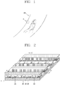
- FIG. 1 is a conceptual view showing a display device using a semiconductor light-emitting element according to an embodiment of the present disclosure.
- information processed in the controller of the display device 100 may be displayed using a flexible display.
- the flexible display may include a flexible, bendable, twistable, foldable and rollable display.
- the flexible display may be a display manufactured on a thin and flexible substrate that can be warped, bent, folded or rolled like a paper sheet while maintaining the display characteristics of a flat display in the related art.
- a display area of the flexible display becomes a plane in a configuration that the flexible display is not warped (for example, a configuration having an infinite radius of curvature, hereinafter, referred to as a "first configuration”).
- the display area thereof becomes a curved surface in a configuration that the flexible display is warped by an external force in the first configuration (for example, a configuration having a finite radius of curvature, hereinafter, referred to as a "second configuration").
- information displayed in the second configuration may be visual information displayed on a curved surface.
- the visual information may be implemented by individually controlling the light emission of sub-pixels disposed in a matrix form.
- the sub-pixel denotes a minimum unit for implementing one color.
- the sub-pixel of the flexible display may be implemented by a semiconductor light-emitting element.
- a light-emitting diode LED
- the light-emitting diode may be formed with a small size to perform the role of a sub-pixel even in the second configuration through this.
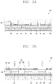
- FIG. 2 is a partial enlarged view of portion "A" in FIG. 1
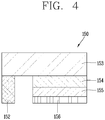
- FIGS. 3A and 3B are cross-sectional views taken along lines B-B and C-C in FIG. 2
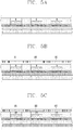
- FIG. 4 is a conceptual view illustrating a flip-chip type semiconductor light-emitting element in FIG. 3A
- FIGS. 5A through 5C are conceptual views illustrating various forms for implementing colors in connection with a flip-chip type semiconductor light-emitting element.
- FIGS. 2 , 3A and 3B there is illustrated a display device 100 using a passive matrix (PM) type semiconductor light-emitting element as a display device 100 using a semiconductor light-emitting element.
- PM passive matrix
- AM active-matrix
- the display device 100 may include a substrate 110, a first electrode 120, a conductive adhesive layer 130, a second electrode 140, and a plurality of semiconductor light-emitting elements 150.
- the substrate 110 may be a flexible substrate.
- the substrate 110 may contain glass or polyimide (PI) to implement the flexible display device.
- PI polyimide
- any one such as polyethylene naphthalate (PEN), polyethylene terephthalate (PET) or the like may be used.
- the substrate 110 may be either one of transparent and non-transparent materials.
- the substrate 110 may be a wiring substrate disposed with the first electrode 120, and thus the first electrode 120 may be placed on the substrate 110.
- an insulating layer 160 may be disposed on the substrate 110 placed with the first electrode 120, and an auxiliary electrode 170 may be placed on the insulating layer 160.
- a state in which the insulating layer 160 is deposited on the substrate 110 may be a single wiring substrate.
- the insulating layer 160 made of an insulating and flexible material such as polyimide (PI), PET, PEN or the like may be integrally formed with the substrate 110 to form a single wiring substrate.
- the auxiliary electrode 170 as an electrode for electrically connecting the first electrode 120 to the semiconductor light-emitting element 150 is placed on the insulating layer 160, and disposed to correspond to the location of the first electrode 120.
- the auxiliary electrode 170 has a dot shape, and may be electrically connected to the first electrode 120 by means of an electrode hole 171 passing through the insulating layer 160.
- the electrode hole 171 may be formed by filling a conductive material in a via hole.
- the conductive adhesive layer 130 may be formed on one surface of the insulating layer 160, but the present disclosure may not be necessarily limited to this.
- the conductive adhesive layer 130 may perform the role of an insulating layer in the structure in which the conductive adhesive layer 130 is disposed on the substrate 110.
- the conductive adhesive layer 130 may be a layer having adhesiveness and conductivity, and to this end, a conductive material and an adhesive material may be mixed on the conductive adhesive layer 130. Furthermore, the conductive adhesive layer 130 may have flexibility, thereby allowing a flexible function in the display device.
- the conductive adhesive layer 130 may be an anisotropic conductive film (ACF), an anisotropic conductive paste, a solution containing conductive particles, and the like.
- ACF anisotropic conductive film
- the conductive adhesive layer 130 may allow electrical interconnection in the z-direction passing through the thickness thereof, but may be configured as a layer having electrical insulation in the horizontal x-y direction thereof. Accordingly, the conductive adhesive layer 130 may be referred to as a z-axis conductive layer (however, hereinafter referred to as a "conductive adhesive layer").
- the anisotropic conductive film is a film with a form in which an anisotropic conductive medium is mixed with an insulating base member, and thus when heat and pressure are applied thereto, only a specific portion thereof may have conductivity by means of the anisotropic conductive medium.
- heat and pressure are applied to the anisotropic conductive film, but other methods may be also available for the anisotropic conductive film to partially have conductivity. The methods may include applying only either one of heat and pressure thereto, UV curing, and the like.
- the anisotropic conductive medium may be conductive balls or particles.
- the anisotropic conductive film is a film with a form in which an anisotropic conductive medium is mixed with an insulating base member, and thus when heat and pressure are applied thereto, only a specific portion thereof may have conductivity by means of the conductive balls.
- the anisotropic conductive film may be in a state in which a core with a conductive material contains a plurality of particles coated by an insulating layer with a polymer material, and in this case, it may have conductivity by means of the core while breaking an insulating layer on a portion to which heat and pressure are applied.
- a core may be transformed to implement a layer having both surfaces to which objects contact in the thickness direction of the film.
- heat and pressure are applied to an anisotropic conductive film as a whole, and electrical connection in the z-axis direction is partially formed by a height difference from a mating object adhered by the use of the anisotropic conductive film.
- an anisotropic conductive film may be in a state containing a plurality of particles in which a conductive material is coated on insulating cores.
- a portion to which heat and pressure are applied may be converted (pressed and adhered) to a conductive material to have conductivity in the thickness direction of the film.
- it may be formed to have conductivity in the thickness direction of the film in which a conductive material passes through an insulating base member in the z-direction.
- the conductive material may have a pointed end portion.
- the anisotropic conductive film may be a fixed array anisotropic conductive film (ACF) configured with a form in which conductive balls are inserted into one surface of the insulating base member.
- ACF fixed array anisotropic conductive film
- the insulating base member is formed of an adhesive material, and the conductive balls are intensively disposed at a bottom portion of the insulating base member, and when heat and pressure are applied thereto, the base member is modified along with the conductive balls, thereby having conductivity in the vertical direction thereof.
- the anisotropic conductive film may be all allowed to have a form in which conductive balls are randomly mixed with an insulating base member or a form configured with a plurality of layers in which conductive balls are disposed at any one layer (double-ACF), and the like.
- the anisotropic conductive paste as a form coupled to a paste and conductive balls may be a paste in which conductive balls are mixed with an insulating and adhesive base material.
- a solution containing conductive particles may be a solution in a form containing conductive particles or nano particles.
- the second electrode 140 is located at the insulating layer 160 to be separated from the auxiliary electrode 170.
- the conductive adhesive layer 130 is disposed on the insulating layer 160 located with the auxiliary electrode 170 and second electrode 140.
- the semiconductor light-emitting element 150 is electrically connected to the first electrode 120 and second electrode 140.
- the semiconductor light-emitting element may be a flip chip type semiconductor light-emitting element.
- the semiconductor light-emitting element may include a p-type electrode 156, a p-type semiconductor layer 155 formed with the p-type electrode 156, an active layer 154 formed on the p-type semiconductor layer 155, an n-type semiconductor layer 153 formed on the active layer 154, and an n-type electrode 152 disposed to be separated from the p-type electrode 156 in the horizontal direction on the n-type semiconductor layer 153.
- the p-type electrode 156 may be electrically connected to the welding portion 179 by the conductive adhesive layer 130
- the n-type electrode 152 may be electrically connected to the second electrode 140.
- the auxiliary electrode 170 may be formed in an elongated manner in one direction to be electrically connected to a plurality of semiconductor light-emitting elements 150.
- the left and right p-type electrodes of the semiconductor light-emitting elements around the auxiliary electrode may be electrically connected to one auxiliary electrode.
- the semiconductor light-emitting element 150 is pressed into the conductive adhesive layer 130, and through this, only a portion between the p-type electrode 156 and auxiliary electrode 170 of the semiconductor light-emitting element 150 and a portion between the n-type electrode 152 and second electrode 140 of the semiconductor light-emitting element 150 have conductivity, and the remaining portion does not have conductivity since there is no push-down of the semiconductor light-emitting element.
- the conductive adhesive layer 130 may form an electrical connection as well as allow a mutual coupling between the semiconductor light-emitting element 150 and the auxiliary electrode 170 and between the semiconductor light-emitting element 150 and the second electrode 140.
- a plurality of semiconductor light-emitting elements 150 constitute a light-emitting array, and a phosphor layer 180 is formed on the light-emitting array.
- the light-emitting device array may include a plurality of semiconductor light-emitting elements with different self-luminance values.
- Each of the semiconductor light-emitting elements 150 constitutes a sub-pixel, and is electrically connected to the first electrode 120.
- the semiconductor light-emitting elements are arranged in several rows, for instance, and each row of the semiconductor light-emitting elements may be electrically connected to any one of the plurality of first electrodes.
- the semiconductor light-emitting elements may be connected in a flip chip form, and thus semiconductor light-emitting elements grown on a transparent dielectric substrate. Furthermore, the semiconductor light-emitting elements may be nitride semiconductor light-emitting elements, for instance.
- the semiconductor light-emitting element 150 may have excellent luminance characteristics, and thus it may be possible to configure individual unit pixels even with a small size thereof.
- a partition wall 190 may be formed between the semiconductor light-emitting elements 150.
- the partition wall 190 may perform the role of dividing individual sub-pixels from one another, and be formed as an integral body with the conductive adhesive layer 130.
- a base member of the anisotropic conductive film may form the partition wall when the semiconductor light-emitting element 150 is inserted into the anisotropic conductive film.
- the partition wall 190 may have reflective characteristics while at the same time increasing contrast with no additional black insulator.
- a reflective partition wall may be separately provided with the partition wall 190.
- the partition wall 190 may include a black or white insulator according to the purpose of the display device.
- a partition wall of a white insulator When a partition wall of a white insulator is used, an effect of enhancing reflectivity may be obtained.
- a partition wall of a black insulator When a partition wall of a black insulator is used, a contrast ratio may be increased while having a reflection characteristic.
- the phosphor layer 180 may be located at an outer surface of the semiconductor light-emitting element 150.
- the semiconductor light-emitting element 150 is a blue semiconductor light-emitting element that emits blue (B) light, and the phosphor layer 180 performs a function of converting the blue (B) light into the color of a sub-pixel.
- the phosphor layer 180 may be a red phosphor layer 181 or green phosphor layer 182 constituting individual pixels.
- a red phosphor 181 capable of converting blue light into red (R) light may be deposited on the blue semiconductor light-emitting element 151 at a position implementing a red sub-pixel
- a green phosphor 182 capable of converting blue light into green (G) light may be deposited on the blue semiconductor light-emitting element 151 at a position implementing a green sub-pixel.
- the blue semiconductor light-emitting element 151 may be solely used at a location implementing a blue sub-pixel.
- the red (R), green (G) and blue (B) sub-pixels may implement one pixel.
- one color phosphor may be deposited along each line of the first electrode 120. Accordingly, one line on the first electrode 120 may be an electrode controlling one color.
- red (R), green (B) and blue (B) may be sequentially disposed along the second electrode 140, thereby implementing sub-pixels.
- the present disclosure may not be necessarily limited to this, and the semiconductor light-emitting element 150 may be combined with quantum dot (QD) instead of phosphor to implement sub-pixels such as red (R), green (G) and blue (B).
- QD quantum dot
- a black matrix 191 may be disposed between each phosphor layer to enhance contrast.
- the black matrix 191 can enhance the contrast of luminance.
- the present disclosure may not be necessarily limited to this, and another structure for implementing blue, red and green may be also applicable thereto.
- each of the semiconductor light-emitting elements 150 may be implemented with a high-power light-emitting device that emits various lights including blue in which gallium nitride (GaN) is mostly used, and indium (In) and or aluminum (Al) are added thereto.
- GaN gallium nitride
- Al aluminum
- the semiconductor light-emitting element 150 may be red, green and blue semiconductor light-emitting elements, respectively, to implement each sub-pixel.
- red, green and blue semiconductor light-emitting elements R, G, B
- red, green and blue sub-pixels implement one pixel by means of the red, green and blue semiconductor light-emitting elements, thereby implementing a full color display.
- the semiconductor light-emitting element may have a white light-emitting device (W) provided with a yellow phosphor layer for each element.
- a red phosphor layer 181, a green phosphor layer 182 and blue phosphor layer 183 may be provided on the white light-emitting device (W) to implement a sub-pixel.
- a color filter repeated with red, green and blue on the white light-emitting device (W) may be used to implement a sub-pixel.
- a red phosphor layer 181, a green phosphor layer 182 and blue phosphor layer 183 may be provided on a ultra violet light-emitting device (UV).
- UV ultra violet light-emitting device
- the semiconductor light-emitting element can be used over the entire region up to ultra violet (UV) as well as visible light, and may be extended to a form of semiconductor light-emitting element in which ultra violet (UV) can be used as an excitation source.
- the semiconductor light-emitting element 150 is placed on the conductive adhesive layer 130 to constitute a sub-pixel in the display device.
- the semiconductor light-emitting element 150 may have excellent luminance characteristics, and thus it may be possible to configure individual sub-pixels even with a small size thereof.
- the size of the individual semiconductor light-emitting element 150 may be less than 80 ⁇ m in the length of one side thereof, and formed with a rectangular or square shaped element. In case of a rectangular shaped element, the size thereof may be less than 20 x 80 ⁇ m.
- a square shaped semiconductor light-emitting element 150 with a length of side of 10 ⁇ m is used for a sub-pixel, it will exhibit a sufficient brightness for implementing a display device. Accordingly, for example, in case of a rectangular pixel in which one side of a sub-pixel is 600 ⁇ m in size, and the remaining one side thereof is 300 ⁇ m, a relative distance between the semiconductor light-emitting elements becomes sufficiently large. Accordingly, in this case, it may be possible to implement a flexible display device having a HD image quality.
- a display device using the foregoing semiconductor light-emitting element will be manufactured by a new type of manufacturing method.
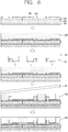
- the manufacturing method will be described with reference to FIG. 6 .
- FIG. 6 is cross-sectional views illustrating a manufacturing method of a display device using a semiconductor light-emitting element according to the present disclosure.
- the conductive adhesive layer 130 is formed on the insulating layer 160 located with the auxiliary electrode 170 and second electrode 140.
- the insulating layer 160 is deposited on the first substrate 110 to form one substrate (or wiring substrate), and the first electrode 120, auxiliary electrode 170 and second electrode 140 are disposed at the wiring substrate.
- the first electrode 120 and second electrode 140 may be disposed in a perpendicular direction to each other.
- the first substrate 110 and insulating layer 160 may contain glass or polyimide (PI), respectively, to implement a flexible display device.
- the conductive adhesive layer 130 may be implemented by an anisotropic conductive film, for example, and to this end, an anisotropic conductive film may be coated on a substrate located with the insulating layer 160.
- a second substrate 112 located with a plurality of semiconductor light-emitting elements 150 corresponding to the location of the auxiliary electrodes 170 and second electrodes 140 and constituting individual pixels is disposed such that the semiconductor light-emitting element 150 faces the auxiliary electrode 170 and second electrode 140.
- the second substrate 112 as a growth substrate for growing the semiconductor light-emitting element 150 may be a sapphire substrate or silicon substrate.
- the semiconductor light-emitting element may have a gap and size capable of implementing a display device when formed in the unit of wafer, and thus effectively used for a display device.
- the wiring substrate is thermally compressed to the second substrate 112.
- the wiring substrate and second substrate 112 may be thermally compressed to each other by applying an ACF press head.
- the wiring substrate and second substrate 112 are bonded to each other using the thermal compression. Only a portion between the semiconductor light-emitting element 150 and the auxiliary electrode 170 and second electrode 140 may have conductivity due to the characteristics of an anisotropic conductive film having conductivity by thermal compression, thereby allowing the electrodes and semiconductor light-emitting element 150 to be electrically connected to each other.
- the semiconductor light-emitting element 150 may be inserted into the anisotropic conductive film, thereby forming a partition wall between the semiconductor light-emitting elements 150.
- the second substrate 112 is removed.
- the second substrate 112 may be removed using a laser lift-off (LLO) or chemical lift-off (CLO) method.
- LLO laser lift-off
- CLO chemical lift-off
- the second substrate 112 is removed to expose the semiconductor light-emitting elements 150 to the outside.
- Silicon oxide (SiOx) or the like may be coated on the wiring substrate coupled to the semiconductor light-emitting element 150 to form a transparent insulating layer (not shown).
- the semiconductor light-emitting element 150 may be a blue semiconductor light-emitting element for emitting blue (B) light, and red or green phosphor for converting the blue (B) light into the color of the sub-pixel may form a layer on one surface of the blue semiconductor light-emitting element.
- the manufacturing method or structure of a display device using the foregoing semiconductor light-emitting element may be modified in various forms.
- the foregoing display device may be applicable to a vertical semiconductor light-emitting element.
- the vertical structure will be described with reference to FIGS. 5 and 6 .
- FIG. 7 is a perspective view illustrating a display device using a semiconductor light-emitting element according to another embodiment of the present disclosure.
- FIG. 8 is a cross-sectional view taken along line C-C in FIG. 7
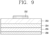
- FIG. 9 is a conceptual view illustrating a vertical type semiconductor light-emitting element in FIG. 8 .
- the display device may be display device using a passive matrix (PM) type of vertical semiconductor light-emitting element.
- PM passive matrix
- the display device may include a substrate 210, a first electrode 220, a conductive adhesive layer 230, a second electrode 240 and a plurality of semiconductor light-emitting elements 250.
- the substrate 210 as a wiring substrate disposed with the first electrode 220 may include polyimide (PI) to implement a flexible display device.
- PI polyimide
- any one may be used if it is an insulating and flexible material.
- the first electrode 220 may be located on the substrate 210, and formed with a bar-shaped electrode elongated in one direction.
- the first electrode 220 may be formed to perform the role of a data electrode.
- the conductive adhesive layer 230 is formed on the substrate 210 located with the first electrode 220. Similar to a display device to which a flip chip type light-emitting device is applied, the conductive adhesive layer 230 may be an anisotropic conductive film (ACF), an anisotropic conductive paste, a solution containing conductive particles, and the like. However, the present embodiment also illustrates a case where the conductive adhesive layer 230 is implemented by an anisotropic conductive film.
- ACF anisotropic conductive film
- the semiconductor light-emitting element 250 When an anisotropic conductive film is located in a state that the first electrode 220 is located on the substrate 210, and then heat and pressure are applied to connect the semiconductor light-emitting element 250 thereto, the semiconductor light-emitting element 250 is electrically connected to the first electrode 220. At this time, the semiconductor light-emitting element 250 may be preferably disposed on the first electrode 220.
- the electrical connection is generated because an anisotropic conductive film partially has conductivity in the thickness direction when heat and pressure are applied as described above. Accordingly, the anisotropic conductive film is partitioned into a portion having conductivity and a portion having no conductivity in the thickness direction thereof.
- anisotropic conductive film contains an adhesive component, and thus the conductive adhesive layer 230 implements a mechanical coupling as well as an electrical coupling between the semiconductor light-emitting element 250 and the first electrode 220.
- the semiconductor light-emitting element 250 is placed on the conductive adhesive layer 230, thereby configuring a separate sub-pixel in the display device.
- the semiconductor light-emitting element 250 may have excellent luminance characteristics, and thus it may be possible to configure individual unit pixels even with a small size thereof.
- the size of the individual semiconductor light-emitting element 250 may be less than 80 ⁇ m in the length of one side thereof, and formed with a rectangular or square shaped element. In case of a rectangular shaped element, the size thereof may be less than 20 x 80 ⁇ m.
- the semiconductor light-emitting element 250 may be a vertical structure.
- a plurality of second electrodes 240 disposed in a direction of crossing the length direction of the first electrode 220, and electrically connected to the vertical semiconductor light-emitting element 250 may be located between vertical semiconductor light-emitting elements.
- the vertical semiconductor light-emitting element may include a p-type electrode 256, a p-type semiconductor layer 255 formed with the p-type electrode 256, an active layer 254 formed on the p-type semiconductor layer 255, an n-type semiconductor layer 253 formed on the active layer 254, and an n-type electrode 252 formed on the n-type semiconductor layer 253.
- the p-type electrode 256 located at the bottom thereof may be electrically connected to the first electrode 220 by the conductive adhesive layer 230
- the n-type electrode 252 located at the top thereof may be electrically connected to the second electrode 240 which will be described later.
- the electrodes may be disposed in the upward/downward direction in the vertical semiconductor light-emitting element 250, thereby providing a great advantage capable of reducing the chip size.
- a phosphor layer 280 may be formed on one surface of the semiconductor light-emitting element 250.
- the semiconductor light-emitting element 250 is a blue semiconductor light-emitting element 251 that emits blue (B) light
- the phosphor layer 280 for converting the blue (B) light into the color of the sub-pixel may be provided thereon.
- the phosphor layer 280 may be a red phosphor 281 and a green phosphor 282 constituting individual pixels.
- a red phosphor 281 capable of converting blue light into red (R) light may be deposited on the blue semiconductor light-emitting element 251 at a position implementing a red sub-pixel
- a green phosphor 282 capable of converting blue light into green (G) light may be deposited on the blue semiconductor light-emitting element 251 at a position implementing a green sub-pixel.
- the blue semiconductor light-emitting element 251 may be solely used at a location implementing a blue sub-pixel. In this case, the red (R), green (G) and blue (B) sub-pixels may implement one pixel.
- the present disclosure may not be necessarily limited to this, and another structure for implementing blue, red and green may be also applicable thereto as described above in a display device to which a flip chip type light-emitting device is applied.
- the second electrode 240 is located between the semiconductor light-emitting elements 250, and electrically connected to the semiconductor light-emitting elements 250.
- the semiconductor light-emitting elements 250 may be disposed in a plurality of rows, and the second electrode 240 may be located between the rows of the semiconductor light-emitting elements 250.
- the second electrode 240 may be located between the semiconductor light-emitting elements 250.
- the second electrode 240 may be formed with a bar-shaped electrode elongated in one direction, and disposed in a perpendicular direction to the first electrode.
- the second electrode 240 may be electrically connected to the semiconductor light-emitting element 250 by a connecting electrode protruded from the second electrode 240.
- the connecting electrode may be an n-type electrode of the semiconductor light-emitting element 250.
- the n-type electrode is formed with an ohmic electrode for ohmic contact, and the second electrode covers at least part of the ohmic electrode by printing or deposition.
- the second electrode 240 may be electrically connected to the n-type electrode of the semiconductor light-emitting element 250.
- the second electrode 240 may be located on the conductive adhesive layer 230.
- a transparent insulating layer (not shown) containing silicon oxide (SiOx) may be formed on the substrate 210 formed with the semiconductor light-emitting element 250.
- SiOx silicon oxide
- the second electrode 240 may be located on the transparent insulating layer.
- the second electrode 240 may be formed to be separated from the conductive adhesive layer 230 or transparent insulating layer.
- a transparent electrode such as indium tin oxide (ITO) is used to locate the second electrode 240 on the semiconductor light-emitting element 250
- the ITO material has a problem of bad adhesiveness with an n-type semiconductor. Accordingly, the second electrode 240 may be placed between the semiconductor light-emitting elements 250, thereby obtaining an advantage in which the transparent electrode is not required. Accordingly, an n-type semiconductor layer and a conductive material having a good adhesiveness may be used as a horizontal electrode without being restricted by the selection of a transparent material, thereby enhancing the light extraction efficiency.
- a partition wall 290 may be formed between the semiconductor light-emitting elements 250.
- the partition wall 290 may be disposed between the vertical semiconductor light-emitting elements 250 to isolate the semiconductor light-emitting element 250 constituting individual pixels.
- the partition wall 290 may perform the role of dividing individual sub-pixels from one another, and be formed as an integral body with the conductive adhesive layer 230.
- a base member of the anisotropic conductive film may form the partition wall when the semiconductor light-emitting element 250 is inserted into the anisotropic conductive film.
- the partition wall 290 may have reflective characteristics while at the same time increasing contrast with no additional black insulator.
- a reflective partition wall may be separately provided with the partition wall 290.
- the partition wall 290 may include a black or white insulator according to the purpose of the display device.
- the partition wall 290 may be located between the semiconductor light-emitting element 250 and second electrode 240. Accordingly, individual unit pixels may be configured even with a small size using the semiconductor light-emitting element 250, and a distance between the semiconductor light-emitting elements 250 may be relatively sufficiently large to place the second electrode 240 between the semiconductor light-emitting elements 250, thereby having the effect of implementing a flexible display device having a HD image quality.
- a black matrix 291 may be disposed between each phosphor layer to enhance contrast.
- the black matrix 291 can enhance the contrast of luminance.
- the semiconductor light-emitting element 250 is located on the conductive adhesive layer 230, thereby constituting individual pixels on the display device.
- the semiconductor light-emitting element 250 may have excellent luminance characteristics, and thus it may be possible to configure individual unit pixels even with a small size thereof. As a result, it may be possible to implement a full color display in which the sub-pixels of red (R), green (G) and blue (B) implement one pixel by means of the semiconductor light-emitting element.
- a process of separating the semiconductor light-emitting element from the growth substrate is performed.
- the semiconductor light-emitting element has been separated from the growth substrate through a laser lift-off method.
- a laser lift-off process of attaching a sapphire substrate on which the formation of a blue semiconductor light-emitting element is completed to a primary donor substrate, and then irradiating a 248-nm or 266-nm excimer laser on the sapphire substrate surface for each semiconductor light-emitting element isolated in a small size to separate a GaN layer between a buffer layer and the sapphire (Al 2 O 3 ) layer is carried out.
- Ga metal remains at a GaN interface, and a process of removing the Ga metal using an acid or a base is additionally performed since the metal layer inhibits the light transmittance of the semiconductor light-emitting element.
- the surface light source When manufacturing a flexible surface light source, the surface light source is manufactured by attaching a small LED chip to a flexible organic material, and thus a laser lift process and a coating or deposition process of an insulating protective layer for an n-GaN or undoped GaN material exposed after removing residual Ga does not exist. Due to this problem, the efficiency deterioration and defect of the blue semiconductor light-emitting element, which is an inorganic material, occurs in a high temperature and high humidity environment.
- the present disclosure provides a structure including an insulating layer capable of protecting n-GaN or undoped GaN exposed to the outside during a laser lift-off process and a method of generating an insulating layer.
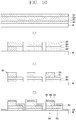
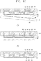
- FIGS. 10 through 12 are conceptual views showing a method of manufacturing a display device according to the present disclosure.
- a step of forming a plurality of semiconductor light-emitting elements on a growth substrate (W) is carried out.
- a buffer layer 360, a second conductive semiconductor layer 353, an active layer 354, and a first conductive semiconductor layer 355 may be sequentially deposited on a growth substrate (W), and then individual semiconductor light-emitting elements may be manufactured through an isolation and mesa process.
- the growth substrate (W) is a sapphire substrate, and a buffer layer, an undoped GaN layer, an n-GaN layer, a GaN MQWs layer, an InGaN layer, and a p-GaN layer may be sequentially deposited on the sapphire substrate, and then semiconductor light-emitting elements may be manufactured.
- the GaN MQWs layer and the InGaN layer may be referred to as active layers.
- the buffer layer and the undoped GaN layer may be made of the same material, and the two layers may not be distinguished.
- a step of form ing conductive electrodes 352 and 356 on the surface of the semiconductor light-emitting element is carried out.
- the conductive electrodes 352 and 356 are formed on the first and second conductive semiconductor layers 353 and 355, respectively.
- the conductive electrodes 352 and 356 may be formed by a vapor deposition method, but the method of forming the conductive electrodes 352 and 356 is not additionally limited.
- a material constituting the passivation layer 370 may include a dielectric material or a metal oxide material.
- the passivation layer 370 may be formed of any one of SiO2, SiOx, SiNx, ZnO, Al 2 O 3 , WOx, MoOx, TiO 2 , NiO, CuOx, and HfOx.
- a step of bonding the growth substrate (W) on which the semiconductor light-emitting element 350 is formed to a temporary substrate 400 is carried out.
- a surface on which the semiconductor light-emitting element is formed between both surfaces of the growth substrate (W) is brought into contact with the temporary substrate 400.
- the temporary substrate 400 may be an organic adhesive layer made of PSA or PDMS, but is not limited thereto.
- the temporary substrate 400 serves to protect the semiconductor light-emitting element 350 while at the same time serving as a donor substrate to transfer the semiconductor light-emitting element 350 to another substrate.
- the growth substrate (W) may be removed using a laser lift-off (LLO) method.
- LLO laser lift-off
- the semiconductor light-emitting element is separated from the growth substrate (W) while part of the buffer layer is destroyed.
- a part 360' of the buffer layer remains on a surface of the semiconductor light-emitting element 350, and the other part 360'" thereof remains on the growth substrate (W).
- the buffer layer 360 absorbs laser light, gas is generated in the buffer layer, and a part of the buffer layer 360 is destroyed by the gas.
- the buffer layer 360 may be split into two layers. Through this, the semiconductor light-emitting element 350 and the growth substrate (W) are separated.
- the buffer layer 360 When the buffer layer 360 is made of GaN, the buffer layer 360 absorbs laser light to emit nitrogen gas, and the semiconductor light-emitting element is separated from the growth substrate (W). In this process, a Ga metal layer 361 is formed on a surface of the buffer layer 360' remaining in the semiconductor light-emitting element 350.
- a metal layer 361 may be formed on the surface of the buffer layer 360' remaining in the semiconductor light-emitting element 350.
- the present disclosure includes a process of oxidizing a metal layer generated after performing the above-described laser lift-off process.
- the step of oxidizing the metal layer 361 may be performed by irradiating the metal layer 361 with a laser.
- the laser is a He-Cd laser, and laser may be irradiated while the semiconductor light-emitting element is immersed in a pH 3.5 phosphoric acid solution or a pH 11 to 13 potassium hydroxide solution to oxidize the Ga metal layer. Accordingly, the Ga metal layer 361 is oxidized to Ga 2 O 3 .
- a thickness of the metal oxide layer is preferably 100 to 500 nm.
- a specific resistance value of the metal oxide layer must be greater than that of the conductive semiconductor layer.
- a specific resistance value, which is an electrical characteristic, of Ga 2 O 3 is 1 E10 ⁇ cm, which can significantly reduce electrical leakage in a panel operating environment (high-temperature high-humidity).
- a step of forming the metal oxide layer may be performed after forming nanopores on a surface of the buffer layer. Specifically, the step of forming nanopores on the surface of the buffer layer may be performed after separating the semiconductor light-emitting element from the growth substrate (W).
- the step of forming nanopores may be performed through electrolysis. Specifically, when a voltage is applied while the buffer layer is immersed in an electrolyte solution, a material constituting the buffer layer is decomposed to form nanopores.
- the GaN layer when electrolyzing a buffer layer made of GaN, nanopores are generated while generating Ga metal and N 2 gas.
- the GaN layer must be doped with dopants having a predetermined concentration.
- electrolysis may not occur well.
- nanopores are formed in a direction toward the conductive semiconductor layer formed under the buffer layer.
- the size and number of nanopores may vary.
- a depth of the nanopores is preferably 0.5 to 1 ⁇ m, and a particle size of the nanopores is preferably 50 to 100 nm.
- the metal layer formed on the surface of the buffer layer is removed. Accordingly, the surface of the buffer layer and an inner wall of the nanopores are made of a material forming the buffer layer.
- the buffer layer is GaN
- the surface of the buffer layer and the inner wall of the nanopores are made of GaN during electrolysis.
- an electrochemical reaction may be performed.
- the electrochemical reaction may be performed by irradiating light having a predetermined wavelength while the buffer layer is immersed in a predetermined solution.
- the buffer layer is made of GaN
- the buffer layer is irradiated with UV light while being immersed in an electrolyte solution
- the surface of the buffer layer and the inner wall of the nanopores are oxidized to Ga 2 O 3 .
- a metal oxide layer is formed on the surface of the buffer layer including the inner wall of the nanopores.
- the above-described metal oxide layer may insulate the conductive semiconductor layer and the buffer layer, thereby preventing current leakage through the buffer layer in a high-temperature and high-humidity environment.
- FIG. 14 is a conceptual view showing a cross section of a semiconductor light-emitting element according to the present disclosure.
- the plurality of semiconductor light-emitting elements 350 included in a display device according to the present disclosure include a buffer layer 360 and a metal oxide layer 380 formed on the buffer layer 360.
- the metal oxide layer 380 is made of an oxide of the buffer layer 360.
- the metal oxide layer 380 is formed by oxidizing the buffer layer 360 itself, or by oxidizing a reduction product of the buffer layer 360.
- the metal oxide layer is formed by oxidizing a Ga metal layer or by oxidizing GaN itself.
- the metal oxide layer may be formed of Ga 2 O 3 .
- the semiconductor light-emitting element 350 includes a first conductive semiconductor layer 355 formed on the wiring electrode, an active layer 354 deposited on the first conductive semiconductor layer 355, and a second conductive semiconductor layer 353 deposited on the active layer 354, and the buffer layer 360 is deposited on the second conductive semiconductor layer 353.
- the semiconductor light-emitting element 350 described below is a flip-chip type semiconductor light-emitting element described in FIG. 4 , but the structure according to the present disclosure may also be applied to a vertical semiconductor light-emitting element.
- the buffer layer 360 is formed on one surface of the second conductive semiconductor layer 353.
- the buffer layer 360 is a layer remaining on the semiconductor light-emitting element 360 after lifting off the semiconductor light-emitting element 350 from the growth substrate (W).
- the buffer layer 360 may be an undoped semiconductor layer or a semiconductor layer doped with dopants having a relatively small concentration compared to the first and second conductive semiconductor layers.
- the metal oxide layer 380 is formed on a surface different from a surface in contact with the second conductive semiconductor layer 353 between both sides of the buffer layer 360
- a material constituting the metal oxide layer 380 may vary depending on the material constituting the buffer layer 360.
- the metal oxide layer 380 may be formed of any one of gallium oxide, silicon oxide, aluminum oxide, silicon carbide, and titanium oxide.
- the buffer layer 360 may include a plurality of nanopores 362.
- the nanopores 362 are formed on a surface in contact with the metal oxide layer 380 between both surfaces of the buffer layer 360.
- the nanopores 362 have a particle size of 50 to 100 nm, and are preferably formed with a depth of 0.5 to 1 ⁇ m in a direction from the surface of the buffer layer 360 toward the second conductive semiconductor layer 353.
- the metal oxide layer 380 is also formed on an inner wall of the nanopores 362. Accordingly, light emitted from the active layer 354 of the semiconductor light-emitting element 350 to the outside through the second conductive semiconductor layer passes through the metal oxide layer 380.
- the display device may further include a light-transmitting layer covering the semiconductor light-emitting elements 350 in order to improve planarization and light uniformity. Due to a difference in refractive index between the conductive semiconductor layer and the light-transmitting layer, total reflection may occur at an interface between the semiconductor light-emitting element and the light-transmitting layer. This causes a decrease in the light efficiency of the display device.
- a refractive index of the metal oxide layer 380 may be between those of the light-transmitting layer and the second conductive semiconductor layer. In this case, the metal oxide layer 380 reduces total reflection occurring at an interface between the semiconductor light-emitting element and the light-transmitting layer, thereby increasing the light efficiency of the display device.
- a thickness of the metal oxide layer 380 is preferably 100 to 500 nm.
- a specific resistance value of the metal oxide layer 380 must be greater than that of the conductive semiconductor layer.
- a specific resistance value, which is an electrical characteristic, of Ga 2 O 3 is 1 E10 ⁇ cm, which can significantly reduce electrical leakage in a panel operating environment (high-temperature high-humidity).
- a passivation layer 370 may be formed on the surface of the semiconductor light-emitting element 350.
- the passivation layer 370 is formed to cover a side surface of the semiconductor light-emitting element 350, which is a surface that is not covered by a conductive electrode.
- the metal oxide layer 380 is not covered by the passivation layer 370.
- a metal layer formed on a surface of the semiconductor light-emitting element may be oxidized by a laser lift-off method, thereby removing the metal layer without exposing the semiconductor light-emitting element to an acid or a base.
- a metal layer formed on a surface of the semiconductor light-emitting element may be oxidized by a laser lift-off method, thereby insulating the surface of the semiconductor light-emitting element exposed to the outside by the laser lift-off method without adding a process of forming an additional insulating layer.
Landscapes
- Electroluminescent Light Sources (AREA)
- Led Device Packages (AREA)
- Devices For Indicating Variable Information By Combining Individual Elements (AREA)
Applications Claiming Priority (2)
| Application Number | Priority Date | Filing Date | Title |
|---|---|---|---|
| US201862776460P | 2018-12-06 | 2018-12-06 | |
| PCT/KR2019/017154 WO2020116978A1 (fr) | 2018-12-06 | 2019-12-06 | Dispositif d'affichage utilisant des éléments électroluminescents à semi-conducteur et son procédé de fabrication |
Publications (3)
| Publication Number | Publication Date |
|---|---|
| EP3893280A1 true EP3893280A1 (fr) | 2021-10-13 |
| EP3893280A4 EP3893280A4 (fr) | 2022-09-14 |
| EP3893280B1 EP3893280B1 (fr) | 2025-03-12 |
Family
ID=70973626
Family Applications (1)
| Application Number | Title | Priority Date | Filing Date |
|---|---|---|---|
| EP19893669.2A Active EP3893280B1 (fr) | 2018-12-06 | 2019-12-06 | Dispositif d'affichage utilisant des éléments électroluminescents à semi-conducteur et son procédé de fabrication |
Country Status (3)
| Country | Link |
|---|---|
| US (1) | US12062734B2 (fr) |
| EP (1) | EP3893280B1 (fr) |
| WO (1) | WO2020116978A1 (fr) |
Families Citing this family (2)
| Publication number | Priority date | Publication date | Assignee | Title |
|---|---|---|---|---|
| WO2024096154A1 (fr) * | 2022-11-02 | 2024-05-10 | 엘지전자 주식회사 | Élément électroluminescent à semi-conducteur et dispositif d'affichage |
| WO2024192126A1 (fr) * | 2023-03-15 | 2024-09-19 | Applied Materials, Inc. | Traitement de métal liquide résiduel pendant la fabrication de del |
Family Cites Families (16)
| Publication number | Priority date | Publication date | Assignee | Title |
|---|---|---|---|---|
| JP3906653B2 (ja) | 2000-07-18 | 2007-04-18 | ソニー株式会社 | 画像表示装置及びその製造方法 |
| US6562644B2 (en) * | 2000-08-08 | 2003-05-13 | Matsushita Electric Industrial Co., Ltd. | Semiconductor substrate, method of manufacturing the semiconductor substrate, semiconductor device and pattern forming method |
| JP3787635B2 (ja) | 2003-09-26 | 2006-06-21 | 国立大学法人東北大学 | 発光素子及びその製造方法 |
| TWM255518U (en) * | 2004-04-23 | 2005-01-11 | Super Nova Optoelectronics Cor | Vertical electrode structure of Gallium Nitride based LED |
| KR20060010331A (ko) | 2004-07-28 | 2006-02-02 | 삼성전자주식회사 | 표시장치 및 이의 제조방법 |
| KR100735488B1 (ko) | 2006-02-03 | 2007-07-04 | 삼성전기주식회사 | 질화갈륨계 발광다이오드 소자의 제조방법 |
| JPWO2009054088A1 (ja) * | 2007-10-23 | 2011-03-03 | パナソニック株式会社 | 半導体発光素子およびそれを用いた半導体発光装置とその製造方法 |
| JP5529420B2 (ja) * | 2009-02-09 | 2014-06-25 | 住友電気工業株式会社 | エピタキシャルウエハ、窒化ガリウム系半導体デバイスを作製する方法、窒化ガリウム系半導体デバイス、及び酸化ガリウムウエハ |
| KR100993074B1 (ko) | 2009-12-29 | 2010-11-08 | 엘지이노텍 주식회사 | 발광소자, 발광소자의 제조방법 및 발광소자 패키지 |
| US20110176301A1 (en) * | 2010-01-21 | 2011-07-21 | Dsem Holdings Sdn. Bhd. | Method to produce homogeneous light output by shaping the light conversion material in multichip module |
| KR101781505B1 (ko) | 2010-10-15 | 2017-09-26 | 엘지디스플레이 주식회사 | 질화갈륨계 반도체 발광소자 및 그 제조방법 |
| US20130140517A1 (en) * | 2011-06-29 | 2013-06-06 | Purdue Research Foundation | Thin and Flexible Gallium Nitride and Method of Making the Same |
| CN103305909B (zh) | 2012-03-14 | 2016-01-20 | 东莞市中镓半导体科技有限公司 | 一种用于GaN生长的复合衬底的制备方法 |
| TWI520376B (zh) | 2013-12-06 | 2016-02-01 | 隆達電子股份有限公司 | 發光二極體元件的製造方法 |
| KR102200027B1 (ko) | 2014-06-23 | 2021-01-11 | 엘지이노텍 주식회사 | 발광소자 및 조명시스템 |
| KR102481524B1 (ko) | 2016-01-11 | 2022-12-26 | 엘지전자 주식회사 | 반도체 발광 소자를 이용한 디스플레이 장치 |
-
2019
- 2019-12-06 US US17/297,874 patent/US12062734B2/en active Active
- 2019-12-06 EP EP19893669.2A patent/EP3893280B1/fr active Active
- 2019-12-06 WO PCT/KR2019/017154 patent/WO2020116978A1/fr not_active Ceased
Also Published As
| Publication number | Publication date |
|---|---|
| EP3893280A4 (fr) | 2022-09-14 |
| US20220037554A1 (en) | 2022-02-03 |
| WO2020116978A1 (fr) | 2020-06-11 |
| EP3893280B1 (fr) | 2025-03-12 |
| US12062734B2 (en) | 2024-08-13 |
Similar Documents
| Publication | Publication Date | Title |
|---|---|---|
| US12074147B2 (en) | Display device using semiconductor light-emitting element and manufacturing method therefor | |
| EP3406110B1 (fr) | Dispositif d'affichage utilisant un dispositif électroluminescent à semi-conducteurs | |
| US9406656B2 (en) | Display device using semiconductor light emitting device and method of fabricating the same | |
| US10446529B2 (en) | Display device using semiconductor light emitting device | |
| EP3079171B1 (fr) | System de transfert incluant une tête de transfert d'un dispositif électro-luminescent à semi-conducteur et procédé correspondant | |
| US9799634B2 (en) | Display device using semiconductor light emitting device | |
| EP3093834B1 (fr) | Dispositif d'affichage utilisant un dispositif électroluminescent à semi-conducteur et son procédé de fabrication | |
| US9831222B2 (en) | Display device using semiconductor light emitting device and method for manufacturing the same | |
| US9666765B2 (en) | Display device using semiconductor light emitting device and method of manufacturing the same | |
| EP3084748B1 (fr) | Dispositif d'affichage utilisant un dispositif électroluminescent à semi-conducteurs et son procédé de fabrication | |
| US11990565B2 (en) | Display device using semiconductor light-emitting diodes | |
| US11658203B2 (en) | Display apparatus using semiconductor light-emitting device | |
| US20180277589A1 (en) | Display device using semiconductor light emitting device | |
| EP4068370B1 (fr) | Appareil d'affichage utilisant un dispositif électroluminescent à semi-conducteur et son procédé de fabrication | |
| US12237359B2 (en) | Display apparatus using semiconductor light-emitting device | |
| EP3893280B1 (fr) | Dispositif d'affichage utilisant des éléments électroluminescents à semi-conducteur et son procédé de fabrication | |
| US10276632B2 (en) | Display device using semiconductor light-emitting diodes, and manufacturing method therefor | |
| US12166154B2 (en) | Display device employing semiconductor light-emitting element and manufacturing method therefor | |
| KR102546499B1 (ko) | 반도체 발광 소자를 이용한 디스플레이 장치 |
Legal Events
| Date | Code | Title | Description |
|---|---|---|---|
| STAA | Information on the status of an ep patent application or granted ep patent |
Free format text: STATUS: THE INTERNATIONAL PUBLICATION HAS BEEN MADE |
|
| PUAI | Public reference made under article 153(3) epc to a published international application that has entered the european phase |
Free format text: ORIGINAL CODE: 0009012 |
|
| STAA | Information on the status of an ep patent application or granted ep patent |
Free format text: STATUS: REQUEST FOR EXAMINATION WAS MADE |
|
| 17P | Request for examination filed |
Effective date: 20210705 |
|
| AK | Designated contracting states |
Kind code of ref document: A1 Designated state(s): AL AT BE BG CH CY CZ DE DK EE ES FI FR GB GR HR HU IE IS IT LI LT LU LV MC MK MT NL NO PL PT RO RS SE SI SK SM TR |
|
| DAV | Request for validation of the european patent (deleted) | ||
| DAX | Request for extension of the european patent (deleted) | ||
| A4 | Supplementary search report drawn up and despatched |
Effective date: 20220818 |
|
| RIC1 | Information provided on ipc code assigned before grant |
Ipc: H01L 21/033 20060101ALI20220810BHEP Ipc: H01L 33/58 20100101ALI20220810BHEP Ipc: H01L 33/12 20100101ALI20220810BHEP Ipc: H01L 33/00 20100101ALI20220810BHEP Ipc: H01L 27/15 20060101AFI20220810BHEP |
|
| REG | Reference to a national code |
Ref country code: DE Ref legal event code: R079 Free format text: PREVIOUS MAIN CLASS: H01L0027150000 Ipc: H01L0025075000 Ref document number: 602019067325 Country of ref document: DE |
|
| GRAP | Despatch of communication of intention to grant a patent |
Free format text: ORIGINAL CODE: EPIDOSNIGR1 |
|
| STAA | Information on the status of an ep patent application or granted ep patent |
Free format text: STATUS: GRANT OF PATENT IS INTENDED |
|
| RIC1 | Information provided on ipc code assigned before grant |
Ipc: H01L 33/44 20100101ALN20240919BHEP Ipc: H01L 33/22 20100101ALN20240919BHEP Ipc: H01L 33/00 20100101ALI20240919BHEP Ipc: H01L 25/075 20060101AFI20240919BHEP |
|
| INTG | Intention to grant announced |
Effective date: 20241002 |
|
| REG | Reference to a national code |
Ref country code: DE Ref legal event code: R079 Free format text: PREVIOUS MAIN CLASS: H01L0025075000 Ipc: H10H0029030000 Ref document number: 602019067325 Country of ref document: DE |
|
| GRAJ | Information related to disapproval of communication of intention to grant by the applicant or resumption of examination proceedings by the epo deleted |
Free format text: ORIGINAL CODE: EPIDOSDIGR1 |
|
| STAA | Information on the status of an ep patent application or granted ep patent |
Free format text: STATUS: REQUEST FOR EXAMINATION WAS MADE |
|
| GRAS | Grant fee paid |
Free format text: ORIGINAL CODE: EPIDOSNIGR3 |
|
| STAA | Information on the status of an ep patent application or granted ep patent |
Free format text: STATUS: GRANT OF PATENT IS INTENDED |
|
| GRAP | Despatch of communication of intention to grant a patent |
Free format text: ORIGINAL CODE: EPIDOSNIGR1 |
|
| GRAA | (expected) grant |
Free format text: ORIGINAL CODE: 0009210 |
|
| STAA | Information on the status of an ep patent application or granted ep patent |
Free format text: STATUS: THE PATENT HAS BEEN GRANTED |
|
| INTC | Intention to grant announced (deleted) | ||
| RIC1 | Information provided on ipc code assigned before grant |
Ipc: H10H 20/82 20250101ALN20250116BHEP Ipc: H10H 20/815 20250101ALN20250116BHEP Ipc: H10H 29/01 20250101ALI20250116BHEP Ipc: H10H 29/03 20250101AFI20250116BHEP |
|
| INTG | Intention to grant announced |
Effective date: 20250203 |
|
| AK | Designated contracting states |
Kind code of ref document: B1 Designated state(s): AL AT BE BG CH CY CZ DE DK EE ES FI FR GB GR HR HU IE IS IT LI LT LU LV MC MK MT NL NO PL PT RO RS SE SI SK SM TR |
|
| REG | Reference to a national code |
Ref country code: GB Ref legal event code: FG4D |
|
| REG | Reference to a national code |
Ref country code: CH Ref legal event code: EP |
|
| REG | Reference to a national code |
Ref country code: DE Ref legal event code: R096 Ref document number: 602019067325 Country of ref document: DE |
|
| REG | Reference to a national code |
Ref country code: IE Ref legal event code: FG4D |
|
| PG25 | Lapsed in a contracting state [announced via postgrant information from national office to epo] |
Ref country code: RS Free format text: LAPSE BECAUSE OF FAILURE TO SUBMIT A TRANSLATION OF THE DESCRIPTION OR TO PAY THE FEE WITHIN THE PRESCRIBED TIME-LIMIT Effective date: 20250612 |
|
| PG25 | Lapsed in a contracting state [announced via postgrant information from national office to epo] |
Ref country code: FI Free format text: LAPSE BECAUSE OF FAILURE TO SUBMIT A TRANSLATION OF THE DESCRIPTION OR TO PAY THE FEE WITHIN THE PRESCRIBED TIME-LIMIT Effective date: 20250312 |
|
| PG25 | Lapsed in a contracting state [announced via postgrant information from national office to epo] |
Ref country code: ES Free format text: LAPSE BECAUSE OF FAILURE TO SUBMIT A TRANSLATION OF THE DESCRIPTION OR TO PAY THE FEE WITHIN THE PRESCRIBED TIME-LIMIT Effective date: 20250312 |
|
| REG | Reference to a national code |
Ref country code: LT Ref legal event code: MG9D |
|
| PG25 | Lapsed in a contracting state [announced via postgrant information from national office to epo] |
Ref country code: NO Free format text: LAPSE BECAUSE OF FAILURE TO SUBMIT A TRANSLATION OF THE DESCRIPTION OR TO PAY THE FEE WITHIN THE PRESCRIBED TIME-LIMIT Effective date: 20250612 |
|
| PG25 | Lapsed in a contracting state [announced via postgrant information from national office to epo] |
Ref country code: HR Free format text: LAPSE BECAUSE OF FAILURE TO SUBMIT A TRANSLATION OF THE DESCRIPTION OR TO PAY THE FEE WITHIN THE PRESCRIBED TIME-LIMIT Effective date: 20250312 |
|
| REG | Reference to a national code |
Ref country code: NL Ref legal event code: MP Effective date: 20250312 |
|
| PG25 | Lapsed in a contracting state [announced via postgrant information from national office to epo] |
Ref country code: LV Free format text: LAPSE BECAUSE OF FAILURE TO SUBMIT A TRANSLATION OF THE DESCRIPTION OR TO PAY THE FEE WITHIN THE PRESCRIBED TIME-LIMIT Effective date: 20250312 |
|
| PG25 | Lapsed in a contracting state [announced via postgrant information from national office to epo] |
Ref country code: BG Free format text: LAPSE BECAUSE OF FAILURE TO SUBMIT A TRANSLATION OF THE DESCRIPTION OR TO PAY THE FEE WITHIN THE PRESCRIBED TIME-LIMIT Effective date: 20250312 Ref country code: GR Free format text: LAPSE BECAUSE OF FAILURE TO SUBMIT A TRANSLATION OF THE DESCRIPTION OR TO PAY THE FEE WITHIN THE PRESCRIBED TIME-LIMIT Effective date: 20250613 |
|
| REG | Reference to a national code |
Ref country code: AT Ref legal event code: MK05 Ref document number: 1776110 Country of ref document: AT Kind code of ref document: T Effective date: 20250312 |
|
| PG25 | Lapsed in a contracting state [announced via postgrant information from national office to epo] |
Ref country code: NL Free format text: LAPSE BECAUSE OF FAILURE TO SUBMIT A TRANSLATION OF THE DESCRIPTION OR TO PAY THE FEE WITHIN THE PRESCRIBED TIME-LIMIT Effective date: 20250312 |
|
| PG25 | Lapsed in a contracting state [announced via postgrant information from national office to epo] |
Ref country code: SE Free format text: LAPSE BECAUSE OF FAILURE TO SUBMIT A TRANSLATION OF THE DESCRIPTION OR TO PAY THE FEE WITHIN THE PRESCRIBED TIME-LIMIT Effective date: 20250312 |
|
| PG25 | Lapsed in a contracting state [announced via postgrant information from national office to epo] |
Ref country code: SM Free format text: LAPSE BECAUSE OF FAILURE TO SUBMIT A TRANSLATION OF THE DESCRIPTION OR TO PAY THE FEE WITHIN THE PRESCRIBED TIME-LIMIT Effective date: 20250312 |
|
| PG25 | Lapsed in a contracting state [announced via postgrant information from national office to epo] |
Ref country code: PT Free format text: LAPSE BECAUSE OF FAILURE TO SUBMIT A TRANSLATION OF THE DESCRIPTION OR TO PAY THE FEE WITHIN THE PRESCRIBED TIME-LIMIT Effective date: 20250714 |
|
| PG25 | Lapsed in a contracting state [announced via postgrant information from national office to epo] |
Ref country code: PL Free format text: LAPSE BECAUSE OF FAILURE TO SUBMIT A TRANSLATION OF THE DESCRIPTION OR TO PAY THE FEE WITHIN THE PRESCRIBED TIME-LIMIT Effective date: 20250312 Ref country code: IT Free format text: LAPSE BECAUSE OF FAILURE TO SUBMIT A TRANSLATION OF THE DESCRIPTION OR TO PAY THE FEE WITHIN THE PRESCRIBED TIME-LIMIT Effective date: 20250312 |
|
| PG25 | Lapsed in a contracting state [announced via postgrant information from national office to epo] |
Ref country code: AT Free format text: LAPSE BECAUSE OF FAILURE TO SUBMIT A TRANSLATION OF THE DESCRIPTION OR TO PAY THE FEE WITHIN THE PRESCRIBED TIME-LIMIT Effective date: 20250312 |
|
| PG25 | Lapsed in a contracting state [announced via postgrant information from national office to epo] |
Ref country code: EE Free format text: LAPSE BECAUSE OF FAILURE TO SUBMIT A TRANSLATION OF THE DESCRIPTION OR TO PAY THE FEE WITHIN THE PRESCRIBED TIME-LIMIT Effective date: 20250312 Ref country code: CZ Free format text: LAPSE BECAUSE OF FAILURE TO SUBMIT A TRANSLATION OF THE DESCRIPTION OR TO PAY THE FEE WITHIN THE PRESCRIBED TIME-LIMIT Effective date: 20250312 |
|
| PG25 | Lapsed in a contracting state [announced via postgrant information from national office to epo] |
Ref country code: RO Free format text: LAPSE BECAUSE OF FAILURE TO SUBMIT A TRANSLATION OF THE DESCRIPTION OR TO PAY THE FEE WITHIN THE PRESCRIBED TIME-LIMIT Effective date: 20250312 |
|
| PG25 | Lapsed in a contracting state [announced via postgrant information from national office to epo] |
Ref country code: SK Free format text: LAPSE BECAUSE OF FAILURE TO SUBMIT A TRANSLATION OF THE DESCRIPTION OR TO PAY THE FEE WITHIN THE PRESCRIBED TIME-LIMIT Effective date: 20250312 |
|
| PG25 | Lapsed in a contracting state [announced via postgrant information from national office to epo] |
Ref country code: IS Free format text: LAPSE BECAUSE OF FAILURE TO SUBMIT A TRANSLATION OF THE DESCRIPTION OR TO PAY THE FEE WITHIN THE PRESCRIBED TIME-LIMIT Effective date: 20250712 |
|
| REG | Reference to a national code |
Ref country code: DE Ref legal event code: R097 Ref document number: 602019067325 Country of ref document: DE |
|
| PGFP | Annual fee paid to national office [announced via postgrant information from national office to epo] |
Ref country code: DE Payment date: 20251105 Year of fee payment: 7 |
|
| PG25 | Lapsed in a contracting state [announced via postgrant information from national office to epo] |
Ref country code: DK Free format text: LAPSE BECAUSE OF FAILURE TO SUBMIT A TRANSLATION OF THE DESCRIPTION OR TO PAY THE FEE WITHIN THE PRESCRIBED TIME-LIMIT Effective date: 20250312 |
|
| PGFP | Annual fee paid to national office [announced via postgrant information from national office to epo] |
Ref country code: FR Payment date: 20251111 Year of fee payment: 7 |
|
| PLBE | No opposition filed within time limit |
Free format text: ORIGINAL CODE: 0009261 |
|
| STAA | Information on the status of an ep patent application or granted ep patent |
Free format text: STATUS: NO OPPOSITION FILED WITHIN TIME LIMIT |
|
| REG | Reference to a national code |
Ref country code: CH Ref legal event code: L10 Free format text: ST27 STATUS EVENT CODE: U-0-0-L10-L00 (AS PROVIDED BY THE NATIONAL OFFICE) Effective date: 20260121 |
|
| 26N | No opposition filed |
Effective date: 20251215 |