EP3893329B1 - Antenne pour envoyer et/ou recevoir des signaux électromagnétiques - Google Patents
Antenne pour envoyer et/ou recevoir des signaux électromagnétiques Download PDFInfo
- Publication number
- EP3893329B1 EP3893329B1 EP20168944.5A EP20168944A EP3893329B1 EP 3893329 B1 EP3893329 B1 EP 3893329B1 EP 20168944 A EP20168944 A EP 20168944A EP 3893329 B1 EP3893329 B1 EP 3893329B1
- Authority
- EP
- European Patent Office
- Prior art keywords
- antenna
- ground
- plane
- feed point
- ground structure
- Prior art date
- Legal status (The legal status is an assumption and is not a legal conclusion. Google has not performed a legal analysis and makes no representation as to the accuracy of the status listed.)
- Active
Links
Images


Classifications
-
- H—ELECTRICITY
- H01—ELECTRIC ELEMENTS
- H01Q—ANTENNAS, i.e. RADIO AERIALS
- H01Q9/00—Electrically-short antennas having dimensions not more than twice the operating wavelength and consisting of conductive active radiating elements
- H01Q9/04—Resonant antennas
- H01Q9/30—Resonant antennas with feed to end of elongated active element, e.g. unipole
- H01Q9/42—Resonant antennas with feed to end of elongated active element, e.g. unipole with folded element, the folded parts being spaced apart a small fraction of the operating wavelength
- H01Q9/43—Scimitar antennas
-
- H—ELECTRICITY
- H01—ELECTRIC ELEMENTS
- H01Q—ANTENNAS, i.e. RADIO AERIALS
- H01Q9/00—Electrically-short antennas having dimensions not more than twice the operating wavelength and consisting of conductive active radiating elements
- H01Q9/04—Resonant antennas
- H01Q9/30—Resonant antennas with feed to end of elongated active element, e.g. unipole
- H01Q9/42—Resonant antennas with feed to end of elongated active element, e.g. unipole with folded element, the folded parts being spaced apart a small fraction of the operating wavelength
-
- H—ELECTRICITY
- H01—ELECTRIC ELEMENTS
- H01Q—ANTENNAS, i.e. RADIO AERIALS
- H01Q1/00—Details of, or arrangements associated with, antennas
- H01Q1/48—Earthing means; Earth screens; Counterpoises
Definitions
- a dielectric constant ⁇ r of a printed board the antenna may be attached to a dielectric constant ⁇ r of a device housing, or a dielectric constant ⁇ r of electronic equipment.
- Further factors are the location at which the antenna is incorporated and material thicknesses. All these and further parameters are taken into account to achieve an optimal antenna design for one or more applications to provide a faster, smoother and cheaper flow of data transmission while being able to place the antenna anywhere.
- a signal with a predefined energy can be transmitted by the antenna to a base station.
- the antenna radiates with a uniform intensity at least along one plane, for example on the azimuth plane.
- planar inverted F-shaped antennas 800 as shown in Figure 6 were mainly used for such applications.
- the radiation pattern 908 of the PIFA antenna 800 as shown in Figures 6 and 7d is not as isotropic as desirable in many applications.
- An isotropic antenna is a hypothetical antenna that radiates the same intensity of radio waves in all directions.
- the first antenna comprises a first monopole antenna and a loop antenna branched off from the first monopole antenna.
- An end of the loop antenna opposing a branching point at which the loop antenna is branched off from the fist monopole antenna is short-circuited between the feeding point of the first antenna and a feeding point of the second antenna on a ground conductor.
- US 2008/0111745 A1 shows an antenna having a ground plane having an edge and a first antenna element extending substantially parallel to the edge.
- a ground element electrically connects the first antenna element with the ground plane.
- a second antenna element extends substantially parallel to the first antenna element and is disposed between the edge and the first antenna element and is connected at one end of the second antenna element to the first antenna element with the remaining end of the second antenna element located closer to the ground element.
- a third antenna element is disposed so that the first antenna element is between the second antenna element and the third antenna element and the third antenna element extends substantially parallel to the first antenna element, with a rear end electrically connected with the first antenna element and a remaining end of the third antenna element is electrically open.
- US 2016/0049732 A1 shows an antenna comprising a ground portion and a radiating portion.
- the radiating portion includes a feed-in terminal, a T-shaped resonant conductor structure extended from the ground portion, and a ground conductor structure.
- US 2009/0295652 A1 shows a planar antenna, including: a film formed of a planar insulating material; an antenna portion which is a planar conductor on the film; and a ground portion which is a conductor to be grounded, wherein the antenna portion comprises: at least one first short stub; a first antenna element which is connected to the ground portion through the at least one first short stub and whose shape has such an angle that a distance between the first antenna element and the ground portion increases with increasing distance from a feeding point along the ground portion, the feeding point being provided between the first antenna element and the ground portion; a second short stub; and a second antenna element which is connected to the first antenna element through the second short stub.
- US 2015/0155627 A1 shows an antenna element including a radiation element, a feeding element, and a shorting element.
- the radiation element has a first end and a second end, and the second end is open.
- the radiation element has plural bends such that the second end is adjacent to the first end.
- One end of the feeding element is coupled through a capacitive element to a connection point on the radiation element, and the connection point is adjacent to or at the first end.
- Another end of the feeding element is coupled to a signal source.
- the feeding element includes a first segment which is substantially parallel to the edge of the ground element.
- EP 3 188 313 A1 shows a multiband antenna, including a feed point, a ground point, a high-frequency radiator working at a high frequency band, and a low-frequency radiator working at a low frequency band.
- One end of the high-frequency radiator is electrically connected to the feed point, the other end of the high-frequency radiator is electrically connected to the ground point, and an electrical length between the two ends of the high-frequency radiator is half of a wavelength of the high frequency band; the high-frequency radiator is connected, in a first position, to the low-frequency radiator, and a length from the first position to the feed point is less than a length from the first position to the ground point.
- US 2009/0278745 A1 shows a dual-band inverted-F antenna. After being fed in by a signal feed-in portion, a first band signal and a second band signal are wirelessly sent from a first radiation portion and a second radiation portion of a radiation element in one aspect, and transmitted to a ground element through a short-circuit pin in another aspect, so as to achieve the dual-band effect. Meanwhile, a bent structure is designed on the short-circuit pin, such that when the short-circuit pin is employed by the dual-band inverted-F antenna to transmit signals, the interference on the signal transmission/reception of the radiation element will be reduced.
- An aspect of the present invention relates to an antenna for sending and/or receiving electromagnetic signals.
- the antenna comprises an electrically conducting ground structure extending along a plane; a first structure forming a radiator, being electrically conducting; a second structure, being electrically conducting; and a feed point for connecting the antenna with a signal line.
- the antenna may be a printed antenna, or may be manufactured by milling, cutting, etching, etc.
- the antenna may be made out at least in parts of an electrically conducting material, for example, copper, silver, gold, aluminium, a combination thereof, etc.
- the antenna may be fixed on a dielectric substrate material such as FR4.
- FR4 is a common dielectric used in circuit boards as an insulator between a ground plane of a signal line and the signal line.
- a substrate may be important in antenna design to affect a size as well as a bandwidth of the antenna.
- a signal line may be a transmission line like a stripline, a microstrip, a coplanar waveguide, a planar transmission line, etc.
- the feed point may be in direct contact with a conductor of the signal line.
- the feed point may be in contact with the signal line by means of a via, a through-hole plating and/or a wire bonding.
- a first end of the first structure and a first end of the second structure are in electrical contact with each other at the feed point. Further, the ground structure is separated from the feed point by a gap.
- the gap may be filled by air or may be filled by a dielectric. In some implementations the gap may be a physical and/or a spatial gap.
- a second end of the second structure is connected to the ground structure and the second structure comprises a bending portion such that the second structure together with a portion of the ground structure surround an area, in particular an area element, when seen from a direction orthogonal to the plane of the ground structure.
- at least parts of the area (area element) may be empty and/or may be filled by gas, like air, and/or by a dielectric.
- at least parts of the second structure and/or at least parts of the ground structure may be arranged in different planes.
- the area may comprise irregularities and/or bumps, in particular in the direction orthogonal to the plane of the ground structure.
- the antenna has the advantage that it is an easy-to-manufacture and compact antenna showing a uniform radiation characteristic.
- the second structure may comprise a first portion attached to the feed point extending away from the ground structure and a second portion attached to the ground structure extending away from the ground structure, wherein distal ends of the first and second portions may be connected by the bending portion.
- This embodiment may have the effect that the compensation loop is connected to the ground structure.
- the compensation loop may form a resonator. As a result, a uniform radiating antenna may be provided in a compact manner.
- the second structure and the ground structure may form a loop with a gap between the feed point and the ground structure. This may have a positive effect that an unwanted short between the feed point and the ground structure is avoided.
- the antenna may be a planar circuit antenna.
- This may have the advantage that the antenna may be manufactured by etching, milling and further technics known from circuit board manufacturing. Further, the plane structure of a planar circuit antenna may be advantageous in many applications with regard to the size and plane form.
- the first structure is substantially U-shaped. This may have the advantage that the antenna is very compact compared to the wavelength and the radiation pattern of the antenna is very uniform.
- a shorter leg of the U-shaped first structure may be connected with the feed point and a longer leg of the U-shaped radiator is open. This may have the advantage that an overall size of the antenna may be reduced, since the second structure may be arranged subsequently to the shorter leg of the first structure.
- the U-shaped first structure may form a radiator as a whole. This may make the radiation pattern of the antenna more isotropic compared to other antennas.
- the second structure are surrounded from three sides by the first structure. This may have the advantage that a compensation loop formed by the second structure may be arranged in a compact manner in the inner of the shape of the first structure. As a result, the overall outer dimensions of the antenna may be reduced.
- the feed point is a 50 Ohm feed point. This may have an advantage that the antenna can be easily connected to a commonly used 50 Ohm signal line without a matching circuit.
- the first structure may have a first portion, a second portion, and a third portion, wherein the second portion connects an end of the first portion with an end of the third portion; an extension direction of the first portion of the first structure may have a main component in a first direction in a plane parallel to the ground structure; and an extension direction of the third portion may have a main component in a second direction opposite to the first direction.
- all portions, in particular the first portion, the second portion and the third portion, of the first structure may form the radiator. This means in particular that all portions of the radiator may radiate and/or receive electromagnetic waves. This may positively affect the radiation pattern in the extension direction of the first portion.
- the first portion of the first structure and the third portion of the second structure are configured to receive or radiate electromagnetic waves the radiation pattern in the extension direction of the first and the third structure may be more isotropic to each other.
- the second portion and the third portion of the first structure may form a radiator.
- an extension direction of the second portion of the first structure may have a main component in a direction perpendicular to the first and second directions.
- the ground structure may form an edge in at least one of a ground plane of the signal line, a plane of the first structurer, or a plane of the second structure. This may have the advantage that the radiation pattern may be improved.
- the first structure and the second structure may be attached to a dielectric substrate. This may have the advantage that a mechanical stability may be improved. Further, an influence of surrounding parameters on a frequency stability of the antenna may be reduced.
- the surrounding behind and in front of the first and/or the second structure may be free from the ground structure, when seen from the direction orthogonal to the plane of the ground structure. This may have the advantage that an attenuation of the radiation in one direction, namely to a frontside or a backside of the antenna, may be avoided.
- no ground structure may be arranged behind or in front of the first and/or the second structure, when seen from the direction orthogonal to the plane of the ground structure. This may have the advantage that the radiation pattern of the antenna is more uniform.
- the bending portion may comprise a concave bending. In some embodiments a bending of the bending portion may be formed in form of one or more corners.
- the signal processing unit may be a radio frequency (RF) front end.
- the signal line may be a feed line, in particular a 50 ⁇ feed line.
- the signal processing unit, in particular an RF front end may for example comprise a matching circuit, comparator, an oscillator, an analogue-to-digital converter and/or a mixer.
- an antenna according to the invention may be part of an antenna array comprising a plurality of antennas.
- the method may have the advantageous effect that one or more signals may be transmitted (due to reciprocity of an antenna radiated and/or received) with low power independent of the orientation of the antenna.
- energy may be saved and battery runtime may be improved in some embodiments.
- electromagnetic radiation affecting organic tissues can be reduced, which may result in a lower specific absorption rate (SAR).
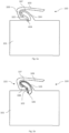
- FIG. 1a shows schematically an example of an antenna according to an embodiment of the invention.
- the antenna 100 comprises an electrically conducting ground structure 101. Further, the antenna comprises a first structure 103, a second structure 104 and a feed point 102.
- the feed point 102 is configured to be connected to a signal line.
- the first structure 103 and the second structure 104 are electrically conducting. A first end of the first structure 103 and a first end of the second structure 104 are in electrical contact with each other at the feed point 102.
- the ground structure 101 is separated from the feed point 102 by a gap 404.
- the gap 404 may be a physical/spatial gap.
- the gap 404 may be filled by gas, like air, and/or may be filled by a dielectric.
- the ground structure being separated from the feed point 102 by the gap 404 may mean that the feed point 102 and the ground structure 101 are not in direct electrical contact with each other at the location of the feed point 102.
- the feed point 102 may be in electrical contact (only) through the first structure, the second structure 104 and a signal line.
- a second end of the second structure 104 is electrically connected to the ground structure 101.
- the second structure comprises a bending portion 107 such that the second structure 104 together with a portion of the ground structure 101 at least substantially surrounds an area (area element) 106 as shown in Figure 1a .
- a frame/encirclement of the area 106 may have a gap 404.
- a frame/encirclement of the area (area element) 106 may be defined, in particular when seen from a direction perpendicular/orthogonal to the plane of the ground structure 101, to the plane of the first structure 103 and/or to the plane of the second structure 104.
- a frame/encirclement of the area (area element) 106 may be defined, in particular when seen from a direction perpendicular/orthogonal to the plane of the ground structure 101, to the plane of the first structure 103 and/or to the plane of the second structure 104.
- the area (area element) 106 may be substantially restricted by the second structure 104 and the ground structure 101 being in electrical contact with the second structure 104.
- the antenna 100 may be a planar circuit antenna and/or a printed circuit antenna.
- the antenna 100 may be attached to a dielectric.
- the antenna may be made at least in parts of copper or a copper alloy or any other electrically conducting material.
- FIG 1b shows schematically an example of an antenna according to an embodiment of the invention.
- the antenna 100 shown in Figure 1b may refer to the antenna 100 shown in Figure 1a .
- the antenna comprises a first structure 103 and a second structure 104, wherein a first end of the first structure 103 is in electrical contact with a first end of the second structure 104 in a feed point 102. A second end of the second structure 104 is in electrical contact with a ground structure 101.
- the first structure 103 and the second structure 104 are both electrically conducting.
- the second structure 104 and the ground structure 101 may form a loop 105 with a gap between the feed point 102 and the ground structure 101.
- the first structure is substantially U-shaped.
- the two "legs" of the U-shaped first structure may or may not have the same length. In some embodiments, the two legs may have different lengths. in particular, a shorter leg 108 of the U-shaped first structure 103 may be in electrical contact with the feed point 102 and/or a longer leg 109 of the U-shaped first structure 103 may be electrical open.
- the second structure 104 are surrounded from three sides by the first structure 103, in particular by the U-shaped first structure 103, in particular, when seen from a direction orthogonal/perpendicular to a plane of the ground structure 101, to a plane of the first structure 103 and/or to a plane of the second structure 104.
- this may mean that at least parts of the second structure 104 are arranged substantially between the two legs, in particular the shorter leg 108 and the longer leg 109, of the substantially U-shaped first structure 103, in particular when seen from a direction orthogonal/perpendicular to a plane of the ground structure 101, to a plane of the first structure 103 and/or to a plane of the second structure 104.
- FIG 2a shows schematically an example of an antenna according to an embodiment of the invention.
- the antenna 100 shown in Figure 2a differs from the antenna 100 shown in Figures 1a and 1b mainly in the form of the second structure 104.
- the bending portion of the antenna 100 shown in Figure 2a comprises corners. Accordingly, one or more corners may replace one or more bendings of a bending portion 107 in some embodiments.
- the first structure 103 may have a first portion 201, a second portion 202 and a third portion 203.
- the second portion 202 may connect an end of the first portion 201 with an end of the third portion 203 electrically.
- An extension direction of the first portion 201 may have a main component in a first direction 204, in particular in parallel to a plane of the ground structure 101 and/or in parallel to an edge 101a of the ground structure 101.
- An extension direction 206 of the third portion 203 may have a main component in a second direction 206 opposite to the first direction 204. in particular, the second direction 206 may be anti-parallel to the first direction 204.
- an extension direction of the second portion 202 of the first structure 103 may have a main component in a direction 205 perpendicular to the first direction 204 and perpendicular to the second direction 206.
- FIG. 2b shows schematically an example of an antenna according to an embodiment of the invention.
- the antenna 100 shown in Figure 2b may refer to the antenna 100 shown in Figure 2a .
- an antenna 100 is shown, wherein the first structure 103 and the second structure 104 are in a plane with a signal line 401.
- the signal line 401 may be, for example, a grounded coplanar waveguide as shown in Figure 2a .
- the signal line may be a microstrip line, a coplanar waveguide, etc. in some embodiments several ground planes/ground structures 101 of the signal line may be connected by one or more vias / through-hole platings 209 to each other.
- the antenna 100 may be attached to a dielectric 402.
- the ground structure 101 may form an edge 101a in at least one of a plane of the first structure 103 and a plane of the second structure 104.
- the first structure 103, the second structure 104 and/or the ground structure 101 may be attached to a dielectric substrate.
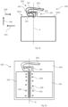
- Figure 3a shows schematically a cross-section of an example of an antenna according to an embodiment of the invention.
- the antenna 100 shown in Figure 3a may relate to the antenna 100 shown in Figure 2a and the cross-section shown in Figure 3a may relate schematically to a cutting plane A shown in Figure 2a .
- the antenna 100 is attached to a dielectric 402. Further, a ground structure 101 and a signal line 401 are attached to the dielectric 402.
- the antenna 100 comprises in accordance with the antennas 100 shown in Figures 1a, 1b , 2a, 2b a first structure 103 and a second structure 104, which are in electrical contact at the feed point 102 not being evident from Figure 3a but from Figures 1a, 1b , 2a, 2b .
- the signal line 401 is in a plane different from a plane of the antenna 100.
- the signal line 401 is electrically connected by one or more vias /through-hole platings 403 to the feed point 102. Further, it is shown that there is a gap 404 between the ground structure 101 and the feed point 102.
- Figure 3b shows schematically a cross section of an example of an antenna according to an embodiment of the invention.
- the antenna 100 shown in Figure 3b may relate to the antenna 100 shown in Figure 2b and a cross-section shown in Figure 3b may relate schematically to a cutting plane B shown in Figure 2b .
- the antenna 100, a ground structure 101 and a signal line 401 may be attached to a dielectric 402.
- the antenna 100 shown in Figure 3b is arranged in a plane with a signal line 401, which is in electrical contact with a feed point 102 of the antenna 100.
- the antenna 100 comprises in accordance with the antennas 100 shown in Figures 1a, 1b , 2a, 2b a first structure 103 and a second structure 104, which are in electrical contact at the feed point 102 not being evident from Figure 3b but from Figures 1a, 1b , 2a, 2b .
- a second end of the second structure 104 may be in electrical contact with the ground structure 101 or may be electrically connected by one or more vias/through-hole platings to the ground structure 101 as shown in Figure 2b .
- a gap 404 between the feed point 102 and the ground structure 101 may be arranged perpendicular to a plane of the antenna 100.
- a complete or at least parts of a surrounding behind and in front of the first and/or the second structure 103, 104 may be free from the ground structure and/or no ground structure may be arranged behind or in front of the first and/or the second structure.
- FIG 4 shows schematically an example of an antenna according to an embodiment of the invention.
- the antenna 100 shown in Figure 4 may refer to an antenna 100 shown in Figure 1 having a centre frequency of 2,4 GHz.
- the antenna 100 may have a horizontal overall size of 18,61 mm and a vertical overall size of 9,23 mm.
- a second end of a first portion 103 of the antenna 100 may be spaced away 10,41 mm in a horizontal direction from a feed point 102 of the antenna 100.
- the ground structure 101 may have a horizontal size of 36 mm. In some embodiments, a vertical size of the ground structure 101 may be of 25 mm.
- FIG. 5 shows schematically an example of an antenna according to an embodiment of the invention.
- the antenna 100 shown in Figure 5 may refer to antennas 100 shown in Figures 2a or 2b having a centre frequency of 2,4 GHz.
- Figure 4 it is shown in Figure 5 that, although the form of the antenna 100 differs, the overall sizes are identical. Namely, the antenna 100 may have a horizontal overall size of 18,61 mm and a vertical overall size of 9,23 mm. Further, it is shown that a second end of a first portion 103 of the antenna 100 may be spaced away 10,41 mm in a horizontal direction from a feed point 102 of the antenna 100.
- the ground structure 101 may have a horizontal size of 36 mm. In some embodiments, a vertical size of the ground structure 101 may be of 25 mm.
- FIG. 6 shows schematically a planar inverted F-shaped antenna (PIFA) as known from the prior art.
- the PIFA antenna 800 comprises a feed point 802, which is electrically connected to a first structure 803 by a feed structure 805 in a section spaced away from ends of the first structure 803.
- the first structure 803 has the function of a radiator.
- the PIFA antenna 800 comprises a second structure 804 being in electrical contact at a first end with a first end of the first structure 803.
- a second end of the second structure 804 is twice in electrical contact with a ground structure 801.
- Figure 7a shows schematically a radiation pattern of the antennas shown in Figures 4, 5 , 6 at a frequency of 2,4 GHz.
- Figure 7b shows an antenna 100 as shown in Figure 4 relative to a coordinate system of the radiation pattern as shown in Figure 7a .
- Figure 7c shows an antenna 100 as shown in Figure 5 relative to the coordinate system of the radiation pattern as shown in Figure 7a .
- Figure 7d shows an antenna 800 as shown in Figure 6 relative to the coordinate system of the radiation pattern as shown in Figure 7a .
- the coordinate systems shown in Figure 7a to 7d comprise a x-direction, a y-direction and a z-direction in the order x-y-z.
- the coordinate systems are right-handed coordinate systems.
- a graph 901 shows a power density in a x-y-plane of the antenna 100 shown in Figure 7b
- a graph 902 shows a power density in the x-y-plane of the antenna 100 shown in Figure 7c
- a graph 908 shows a power density in the x-y-plane of the antenna 800 shown in Figure 7d .
- the power density 908 of a PIFA antenna 800 as shown in Figure 7d is - independent from an azimuth angle - less than the power density 901, 902of the antenna 100. Further, it is shown that the radiation pattern of the PIFA antenna 800 as shown in Figure 7d has in a negative x-direction (at 270°) a value of around-3,8dB and in a positive x-direction (at 90°) a value of around -7dB. As a result, the values of the positive x-direction and negative x-direction of the radiation pattern 908 of the PIFA antenna 800 differ by a value of 3,2dB.
- the radiation pattern 901 of the antenna 100 as shown in Figure 7b has in a negative x-direction (at 270°) a value of around -2,9dB and in a positive x-direction (at 90°) a value of around -4,5dB.
- the values of the positive x-direction and negative x-direction of the radiation pattern 901 of the antenna 100 as shown in Figure 7b differ by a value of around 1,6dB.
- the radiation pattern 902 of the antenna 100 as shown in Figure 7c has in a negative x-direction (at 270°) a value of around -2,1dB and in a positive x-direction (at 90°) a value of around -3,9dB.
- the values of the positive x-direction and negative x-direction of the radiation pattern 902 of the antenna 100 as shown in Figure 7b differ by a value of around 1,8dB.
- an antenna 100 according to the invention may have a more uniform radiation pattern than a PIFA antenna 800 as known from the state of the art.
- FIG 8 shows schematically a process flow of a method according to an embodiment of the invention.
- an antenna 100 in particular an antenna 100 as described in one of Figures 1a, 1b , 2a, 2b , 3a, 3b , 4, 5 , may be provided.
- the antenna 100 may be connected at a feed point 102 with a signal line 401 to a signal processing unit.
- the signal processing unit may generate signals for being transmitted by the antenna 100 and/or the signal processing unit may process signals received by the antenna 100.
- Generating signals for being transmitted by the antenna 100 may also comprise signal processing. Signal processing may be done analogous or digital.
- a signal processing unit may comprise an digital-to-analog converter and/or an analog-to-digital converter.
- the method may have the advantage that transmitting of signals between the antenna 100 and another antenna may be very efficient and robust with regard to noise independent to an relative orientation of the antenna 100 with respect to the another antenna communicating with the antenna 100.
Landscapes
- Details Of Aerials (AREA)
- Aerials With Secondary Devices (AREA)
Claims (11)
- Antenne (100) pour l'envoi et/ou la réception de signaux électromagnétiques, comprenant :une structure de masse électriquement conductrice (101) s'étendant le long d'un plan ;une première structure (103) formant un radiateur, qui est électriquement conductrice ;une seconde structure (104), qui est électriquement conductrice ; etun point d'alimentation (102) pour la connexion de l'antenne à une ligne de signal ;dans laquelleune première extrémité de la première structure (103) et une première extrémité de la seconde structure (104) sont en contact électrique l'une avec l'autre au niveau du point d'alimentation (102),la structure de masse (101) est séparée du point d'alimentation (102) par un espace (404) ;une seconde extrémité de la seconde structure (104) est connectée à la structure de masse (101) ;la seconde structure (104) comprend une portion de cintrage qui est telle que la seconde structure (104) conjointement avec une portion de la structure de masse (101) encerclent une zone lorsqu'on les observe depuis une direction orthogonale au plan de la structure de masse, etla première structure (103) est sensiblement en forme de U,caractérisée en ce queau moins des parties de la seconde structure (104) sont encerclées sur trois côtés par la première structure (103).
- Antenne (100) selon la revendication 1, dans laquellela seconde structure (104) comprend une première portion fixée au point d'alimentation s'étendant en éloignement par rapport à la structure de masse (101) et une deuxième portion fixée à la structure de masse (101) s'étendant en éloignement par rapport à la structure de masse (101), dans laquelle des extrémités distales des première et deuxième portions sont connectées par la portion de cintrage, et/oula seconde structure (104) et la structure de masse (101) forment une boucle avec un espace (404) entre le point d'alimentation (102) et la structure de masse.
- Antenne (100) selon la revendication 1 ou 2, dans laquelle
l'antenne est une antenne à circuit planaire. - Antenne (100) selon l'une des revendications 1 à 3, dans laquelle
une patte plus courte de la première structure en forme de U est connectée au point d'alimentation et une patte plus longue du radiateur en forme de U est ouverte. - Antenne (100) selon l'une des revendications 1 à 4, dans laquelle
le point d'alimentation (102) est un point d'alimentation de 50 Ohms. - Antenne (100) selon l'une des revendications 1 à 5, dans laquellela première structure (103) possède une première portion, une deuxième portion, et une troisième portion, dans laquelle la deuxième portion connecte une extrémité de la première portion à une extrémité de la troisième portion ;une direction d'extension de la première portion de la première structure possède une composante principale dans une première direction dans un plan parallèle à la structure de masse ;une direction d'extension de la troisième portion possède une composante principale dans une seconde direction opposée à la première direction.
- Antenne (100) selon la revendication 6, dans laquelle
une direction d'extension de la deuxième portion de la première structure possède une composante principale dans une direction perpendiculaire aux première et seconde directions. - Antenne (100) selon l'une des revendications 1 à 7, dans laquelle
la structure de masse (101) forme un bord dans au moins l'un parmi un plan de masse de la ligne de signal, un plan de la première structure (103), ou un plan de la seconde structure (104). - Antenne (100) selon l'une des revendications 1 à 8, dans laquelle
la première structure (103) et la seconde structure (104) sont fixées à un substrat diélectrique de l'antenne. - Antenne (100) selon l'une des revendications 1 à 9, dans laquelle,
lorsqu'on les observe depuis la direction orthogonale au plan de la structure de masse (101), l'environnement derrière et devant la première et/ou la seconde structure (103, 104) est exempt de la structure de masse et/ou aucune structure de masse n'est agencée derrière ou devant la première et/ou la seconde structure (103, 104). - Procédé pour l'utilisation d'une antenne pour l'envoi et/ou la réception de signaux électromagnétiques comprenant les étapes de :la fourniture d'une antenne (100) selon l'une des revendications 1 à 10,la connexion de l'antenne à une ligne de signal allant vers une unité de traitement de signal.
Priority Applications (7)
| Application Number | Priority Date | Filing Date | Title |
|---|---|---|---|
| EP20168944.5A EP3893329B1 (fr) | 2020-04-09 | 2020-04-09 | Antenne pour envoyer et/ou recevoir des signaux électromagnétiques |
| DK20168944.5T DK3893329T3 (da) | 2020-04-09 | 2020-04-09 | Antenne til afsendelse og/eller modtagelse af elektromagnetiske signaler |
| PL20168944.5T PL3893329T3 (pl) | 2020-04-09 | 2020-04-09 | Antena dla wysyłania i/lub odbierania sygnałów elektromagnetycznych |
| EP23174723.9A EP4235964A3 (fr) | 2020-04-09 | 2020-04-09 | Antenne pour envoyer et/ou recevoir des signaux électromagnétiques |
| US17/909,381 US12107352B2 (en) | 2020-04-09 | 2021-03-11 | Antenna for sending and/or receiving electromagnetic signals |
| CN202180025123.9A CN115336105A (zh) | 2020-04-09 | 2021-03-11 | 用于发送和/或接收电磁信号的天线 |
| PCT/EP2021/056199 WO2021204491A1 (fr) | 2020-04-09 | 2021-03-11 | Antenne pour émettre et/ou recevoir des signaux électromagnétiques |
Applications Claiming Priority (1)
| Application Number | Priority Date | Filing Date | Title |
|---|---|---|---|
| EP20168944.5A EP3893329B1 (fr) | 2020-04-09 | 2020-04-09 | Antenne pour envoyer et/ou recevoir des signaux électromagnétiques |
Related Child Applications (2)
| Application Number | Title | Priority Date | Filing Date |
|---|---|---|---|
| EP23174723.9A Division EP4235964A3 (fr) | 2020-04-09 | 2020-04-09 | Antenne pour envoyer et/ou recevoir des signaux électromagnétiques |
| EP23174723.9A Division-Into EP4235964A3 (fr) | 2020-04-09 | 2020-04-09 | Antenne pour envoyer et/ou recevoir des signaux électromagnétiques |
Publications (2)
| Publication Number | Publication Date |
|---|---|
| EP3893329A1 EP3893329A1 (fr) | 2021-10-13 |
| EP3893329B1 true EP3893329B1 (fr) | 2023-09-20 |
Family
ID=70285451
Family Applications (2)
| Application Number | Title | Priority Date | Filing Date |
|---|---|---|---|
| EP23174723.9A Pending EP4235964A3 (fr) | 2020-04-09 | 2020-04-09 | Antenne pour envoyer et/ou recevoir des signaux électromagnétiques |
| EP20168944.5A Active EP3893329B1 (fr) | 2020-04-09 | 2020-04-09 | Antenne pour envoyer et/ou recevoir des signaux électromagnétiques |
Family Applications Before (1)
| Application Number | Title | Priority Date | Filing Date |
|---|---|---|---|
| EP23174723.9A Pending EP4235964A3 (fr) | 2020-04-09 | 2020-04-09 | Antenne pour envoyer et/ou recevoir des signaux électromagnétiques |
Country Status (6)
| Country | Link |
|---|---|
| US (1) | US12107352B2 (fr) |
| EP (2) | EP4235964A3 (fr) |
| CN (1) | CN115336105A (fr) |
| DK (1) | DK3893329T3 (fr) |
| PL (1) | PL3893329T3 (fr) |
| WO (1) | WO2021204491A1 (fr) |
Families Citing this family (2)
| Publication number | Priority date | Publication date | Assignee | Title |
|---|---|---|---|---|
| EP4583647A4 (fr) * | 2022-10-07 | 2026-04-22 | Samsung Electronics Co Ltd | Structure de connexion utilisant un élément élastique et dispositif électronique la comprenant |
| CN120184576B (zh) * | 2025-05-20 | 2025-09-05 | 杭州电子科技大学 | 一种基于天线增强器的系统地平面集成准各向同性天线 |
Family Cites Families (16)
| Publication number | Priority date | Publication date | Assignee | Title |
|---|---|---|---|---|
| US6476769B1 (en) * | 2001-09-19 | 2002-11-05 | Nokia Corporation | Internal multi-band antenna |
| US7365689B2 (en) * | 2006-06-23 | 2008-04-29 | Arcadyan Technology Corporation | Metal inverted F antenna |
| JP2008124617A (ja) * | 2006-11-09 | 2008-05-29 | Tyco Electronics Amp Kk | アンテナ |
| US20090278745A1 (en) * | 2008-05-09 | 2009-11-12 | Smart Approach Co., Ltd. | Dual-band inverted-f antenna |
| JP4775406B2 (ja) * | 2008-05-29 | 2011-09-21 | カシオ計算機株式会社 | 平面アンテナ及び電子機器 |
| CN101651253B (zh) * | 2008-08-11 | 2014-09-10 | 深圳富泰宏精密工业有限公司 | 双频天线及应用该双频天线的无线通信装置 |
| TWI448006B (zh) * | 2009-11-20 | 2014-08-01 | Arcadyan Technology Corp | 具多頻帶之天線 |
| CN102934246A (zh) * | 2010-06-09 | 2013-02-13 | 盖尔创尼克斯有限公司 | 单分支多频带天线 |
| TWI430513B (zh) * | 2010-06-23 | 2014-03-11 | Quanta Comp Inc | Dual frequency antenna |
| TWI543444B (zh) * | 2012-08-20 | 2016-07-21 | 鴻海精密工業股份有限公司 | 多頻平面倒f型天線 |
| TWI475747B (zh) * | 2013-10-11 | 2015-03-01 | Acer Inc | 通訊裝置 |
| TWI531115B (zh) * | 2013-12-04 | 2016-04-21 | 宏碁股份有限公司 | 通訊裝置 |
| TWI538310B (zh) * | 2014-01-08 | 2016-06-11 | 智易科技股份有限公司 | 雙頻印刷式的單極天線 |
| TWI543445B (zh) * | 2014-08-12 | 2016-07-21 | 智易科技股份有限公司 | 天線及其製造方法 |
| JP2017532886A (ja) * | 2014-09-25 | 2017-11-02 | 華為技術有限公司Huawei Technologies Co.,Ltd. | マルチバンドアンテナおよび通信端末 |
| WO2017069181A1 (fr) | 2015-10-22 | 2017-04-27 | 株式会社村田製作所 | Dispositif d'antenne |
-
2020
- 2020-04-09 EP EP23174723.9A patent/EP4235964A3/fr active Pending
- 2020-04-09 DK DK20168944.5T patent/DK3893329T3/da active
- 2020-04-09 PL PL20168944.5T patent/PL3893329T3/pl unknown
- 2020-04-09 EP EP20168944.5A patent/EP3893329B1/fr active Active
-
2021
- 2021-03-11 US US17/909,381 patent/US12107352B2/en active Active
- 2021-03-11 WO PCT/EP2021/056199 patent/WO2021204491A1/fr not_active Ceased
- 2021-03-11 CN CN202180025123.9A patent/CN115336105A/zh active Pending
Also Published As
| Publication number | Publication date |
|---|---|
| WO2021204491A1 (fr) | 2021-10-14 |
| CN115336105A (zh) | 2022-11-11 |
| US12107352B2 (en) | 2024-10-01 |
| DK3893329T3 (da) | 2023-10-30 |
| EP4235964A2 (fr) | 2023-08-30 |
| EP4235964A3 (fr) | 2023-10-04 |
| US20230097476A1 (en) | 2023-03-30 |
| PL3893329T3 (pl) | 2024-02-26 |
| EP3893329A1 (fr) | 2021-10-13 |
Similar Documents
| Publication | Publication Date | Title |
|---|---|---|
| US6603430B1 (en) | Handheld wireless communication devices with antenna having parasitic element | |
| US20260051651A1 (en) | Electronic device | |
| US6762724B2 (en) | Build-in antenna for a mobile communication terminal | |
| KR100638661B1 (ko) | 초광대역 내장형 안테나 | |
| KR101044136B1 (ko) | 개방종단 폴디드 슬롯 안테나 | |
| JP5213039B2 (ja) | 片面放射アンテナ | |
| EP3893329B1 (fr) | Antenne pour envoyer et/ou recevoir des signaux électromagnétiques | |
| US7173566B2 (en) | Low-sidelobe dual-band and broadband flat endfire antenna | |
| US8593368B2 (en) | Multi-band antenna and electronic apparatus having the same | |
| JP4125118B2 (ja) | 広帯域内蔵型アンテナ | |
| CN101350445A (zh) | 双谐振三角形贴片天线 | |
| WO2024069858A1 (fr) | Dispositif de transmission et antenne | |
| CN117673705A (zh) | 天线单元及通信设备 | |
| CN117525832A (zh) | 一种天线、感知模块、传感器和电子设备 | |
| CN101728639B (zh) | 多频天线及其具有多频天线的电子装置 | |
| US20210104816A1 (en) | Combination driven and parasitic element circularly polarized antenna | |
| US12062857B2 (en) | Three-dimensional antenna module | |
| CN113964531B (zh) | 一种极小直径宽带偶极子全向天线 | |
| KR102357671B1 (ko) | 모서리 안테나 | |
| CN115775976A (zh) | 天线设备 | |
| KR20180123804A (ko) | 초광대역 평면 안테나 | |
| CN223612686U (zh) | 天线和无线设备 | |
| CN213717050U (zh) | 一种蓝牙天线 | |
| CN115000694B (zh) | 一种小型全向辐射印刷天线 | |
| CN215989221U (zh) | 天线装置及电子设备 |
Legal Events
| Date | Code | Title | Description |
|---|---|---|---|
| PUAI | Public reference made under article 153(3) epc to a published international application that has entered the european phase |
Free format text: ORIGINAL CODE: 0009012 |
|
| STAA | Information on the status of an ep patent application or granted ep patent |
Free format text: STATUS: THE APPLICATION HAS BEEN PUBLISHED |
|
| AK | Designated contracting states |
Kind code of ref document: A1 Designated state(s): AL AT BE BG CH CY CZ DE DK EE ES FI FR GB GR HR HU IE IS IT LI LT LU LV MC MK MT NL NO PL PT RO RS SE SI SK SM TR |
|
| STAA | Information on the status of an ep patent application or granted ep patent |
Free format text: STATUS: REQUEST FOR EXAMINATION WAS MADE |
|
| 17P | Request for examination filed |
Effective date: 20220413 |
|
| RBV | Designated contracting states (corrected) |
Designated state(s): AL AT BE BG CH CY CZ DE DK EE ES FI FR GB GR HR HU IE IS IT LI LT LU LV MC MK MT NL NO PL PT RO RS SE SI SK SM TR |
|
| STAA | Information on the status of an ep patent application or granted ep patent |
Free format text: STATUS: EXAMINATION IS IN PROGRESS |
|
| 17Q | First examination report despatched |
Effective date: 20220713 |
|
| GRAP | Despatch of communication of intention to grant a patent |
Free format text: ORIGINAL CODE: EPIDOSNIGR1 |
|
| STAA | Information on the status of an ep patent application or granted ep patent |
Free format text: STATUS: GRANT OF PATENT IS INTENDED |
|
| INTG | Intention to grant announced |
Effective date: 20221213 |
|
| GRAJ | Information related to disapproval of communication of intention to grant by the applicant or resumption of examination proceedings by the epo deleted |
Free format text: ORIGINAL CODE: EPIDOSDIGR1 |
|
| STAA | Information on the status of an ep patent application or granted ep patent |
Free format text: STATUS: EXAMINATION IS IN PROGRESS |
|
| INTC | Intention to grant announced (deleted) | ||
| GRAP | Despatch of communication of intention to grant a patent |
Free format text: ORIGINAL CODE: EPIDOSNIGR1 |
|
| STAA | Information on the status of an ep patent application or granted ep patent |
Free format text: STATUS: GRANT OF PATENT IS INTENDED |
|
| INTG | Intention to grant announced |
Effective date: 20230510 |
|
| P01 | Opt-out of the competence of the unified patent court (upc) registered |
Effective date: 20230505 |
|
| GRAS | Grant fee paid |
Free format text: ORIGINAL CODE: EPIDOSNIGR3 |
|
| GRAA | (expected) grant |
Free format text: ORIGINAL CODE: 0009210 |
|
| STAA | Information on the status of an ep patent application or granted ep patent |
Free format text: STATUS: THE PATENT HAS BEEN GRANTED |
|
| AK | Designated contracting states |
Kind code of ref document: B1 Designated state(s): AL AT BE BG CH CY CZ DE DK EE ES FI FR GB GR HR HU IE IS IT LI LT LU LV MC MK MT NL NO PL PT RO RS SE SI SK SM TR |
|
| REG | Reference to a national code |
Ref country code: GB Ref legal event code: FG4D |
|
| REG | Reference to a national code |
Ref country code: CH Ref legal event code: EP |
|
| REG | Reference to a national code |
Ref country code: DE Ref legal event code: R096 Ref document number: 602020017846 Country of ref document: DE |
|
| REG | Reference to a national code |
Ref country code: IE Ref legal event code: FG4D |
|
| REG | Reference to a national code |
Ref country code: DK Ref legal event code: T3 Effective date: 20231026 |
|
| REG | Reference to a national code |
Ref country code: NL Ref legal event code: FP |
|
| REG | Reference to a national code |
Ref country code: SE Ref legal event code: TRGR |
|
| REG | Reference to a national code |
Ref country code: LT Ref legal event code: MG9D |
|
| PG25 | Lapsed in a contracting state [announced via postgrant information from national office to epo] |
Ref country code: GR Free format text: LAPSE BECAUSE OF FAILURE TO SUBMIT A TRANSLATION OF THE DESCRIPTION OR TO PAY THE FEE WITHIN THE PRESCRIBED TIME-LIMIT Effective date: 20231221 |
|
| PG25 | Lapsed in a contracting state [announced via postgrant information from national office to epo] |
Ref country code: RS Free format text: LAPSE BECAUSE OF FAILURE TO SUBMIT A TRANSLATION OF THE DESCRIPTION OR TO PAY THE FEE WITHIN THE PRESCRIBED TIME-LIMIT Effective date: 20230920 Ref country code: NO Free format text: LAPSE BECAUSE OF FAILURE TO SUBMIT A TRANSLATION OF THE DESCRIPTION OR TO PAY THE FEE WITHIN THE PRESCRIBED TIME-LIMIT Effective date: 20231220 Ref country code: LV Free format text: LAPSE BECAUSE OF FAILURE TO SUBMIT A TRANSLATION OF THE DESCRIPTION OR TO PAY THE FEE WITHIN THE PRESCRIBED TIME-LIMIT Effective date: 20230920 Ref country code: LT Free format text: LAPSE BECAUSE OF FAILURE TO SUBMIT A TRANSLATION OF THE DESCRIPTION OR TO PAY THE FEE WITHIN THE PRESCRIBED TIME-LIMIT Effective date: 20230920 Ref country code: HR Free format text: LAPSE BECAUSE OF FAILURE TO SUBMIT A TRANSLATION OF THE DESCRIPTION OR TO PAY THE FEE WITHIN THE PRESCRIBED TIME-LIMIT Effective date: 20230920 Ref country code: GR Free format text: LAPSE BECAUSE OF FAILURE TO SUBMIT A TRANSLATION OF THE DESCRIPTION OR TO PAY THE FEE WITHIN THE PRESCRIBED TIME-LIMIT Effective date: 20231221 Ref country code: FI Free format text: LAPSE BECAUSE OF FAILURE TO SUBMIT A TRANSLATION OF THE DESCRIPTION OR TO PAY THE FEE WITHIN THE PRESCRIBED TIME-LIMIT Effective date: 20230920 |
|
| REG | Reference to a national code |
Ref country code: AT Ref legal event code: MK05 Ref document number: 1614149 Country of ref document: AT Kind code of ref document: T Effective date: 20230920 |
|
| PG25 | Lapsed in a contracting state [announced via postgrant information from national office to epo] |
Ref country code: IS Free format text: LAPSE BECAUSE OF FAILURE TO SUBMIT A TRANSLATION OF THE DESCRIPTION OR TO PAY THE FEE WITHIN THE PRESCRIBED TIME-LIMIT Effective date: 20240120 |
|
| PG25 | Lapsed in a contracting state [announced via postgrant information from national office to epo] |
Ref country code: AT Free format text: LAPSE BECAUSE OF FAILURE TO SUBMIT A TRANSLATION OF THE DESCRIPTION OR TO PAY THE FEE WITHIN THE PRESCRIBED TIME-LIMIT Effective date: 20230920 |
|
| PG25 | Lapsed in a contracting state [announced via postgrant information from national office to epo] |
Ref country code: ES Free format text: LAPSE BECAUSE OF FAILURE TO SUBMIT A TRANSLATION OF THE DESCRIPTION OR TO PAY THE FEE WITHIN THE PRESCRIBED TIME-LIMIT Effective date: 20230920 |
|
| PG25 | Lapsed in a contracting state [announced via postgrant information from national office to epo] |
Ref country code: SM Free format text: LAPSE BECAUSE OF FAILURE TO SUBMIT A TRANSLATION OF THE DESCRIPTION OR TO PAY THE FEE WITHIN THE PRESCRIBED TIME-LIMIT Effective date: 20230920 Ref country code: RO Free format text: LAPSE BECAUSE OF FAILURE TO SUBMIT A TRANSLATION OF THE DESCRIPTION OR TO PAY THE FEE WITHIN THE PRESCRIBED TIME-LIMIT Effective date: 20230920 Ref country code: IS Free format text: LAPSE BECAUSE OF FAILURE TO SUBMIT A TRANSLATION OF THE DESCRIPTION OR TO PAY THE FEE WITHIN THE PRESCRIBED TIME-LIMIT Effective date: 20240120 Ref country code: ES Free format text: LAPSE BECAUSE OF FAILURE TO SUBMIT A TRANSLATION OF THE DESCRIPTION OR TO PAY THE FEE WITHIN THE PRESCRIBED TIME-LIMIT Effective date: 20230920 Ref country code: EE Free format text: LAPSE BECAUSE OF FAILURE TO SUBMIT A TRANSLATION OF THE DESCRIPTION OR TO PAY THE FEE WITHIN THE PRESCRIBED TIME-LIMIT Effective date: 20230920 Ref country code: CZ Free format text: LAPSE BECAUSE OF FAILURE TO SUBMIT A TRANSLATION OF THE DESCRIPTION OR TO PAY THE FEE WITHIN THE PRESCRIBED TIME-LIMIT Effective date: 20230920 Ref country code: AT Free format text: LAPSE BECAUSE OF FAILURE TO SUBMIT A TRANSLATION OF THE DESCRIPTION OR TO PAY THE FEE WITHIN THE PRESCRIBED TIME-LIMIT Effective date: 20230920 Ref country code: SK Free format text: LAPSE BECAUSE OF FAILURE TO SUBMIT A TRANSLATION OF THE DESCRIPTION OR TO PAY THE FEE WITHIN THE PRESCRIBED TIME-LIMIT Effective date: 20230920 Ref country code: PT Free format text: LAPSE BECAUSE OF FAILURE TO SUBMIT A TRANSLATION OF THE DESCRIPTION OR TO PAY THE FEE WITHIN THE PRESCRIBED TIME-LIMIT Effective date: 20240122 |
|
| REG | Reference to a national code |
Ref country code: DE Ref legal event code: R097 Ref document number: 602020017846 Country of ref document: DE |
|
| PLBE | No opposition filed within time limit |
Free format text: ORIGINAL CODE: 0009261 |
|
| STAA | Information on the status of an ep patent application or granted ep patent |
Free format text: STATUS: NO OPPOSITION FILED WITHIN TIME LIMIT |
|
| 26N | No opposition filed |
Effective date: 20240621 |
|
| PG25 | Lapsed in a contracting state [announced via postgrant information from national office to epo] |
Ref country code: SI Free format text: LAPSE BECAUSE OF FAILURE TO SUBMIT A TRANSLATION OF THE DESCRIPTION OR TO PAY THE FEE WITHIN THE PRESCRIBED TIME-LIMIT Effective date: 20230920 |
|
| PG25 | Lapsed in a contracting state [announced via postgrant information from national office to epo] |
Ref country code: SI Free format text: LAPSE BECAUSE OF FAILURE TO SUBMIT A TRANSLATION OF THE DESCRIPTION OR TO PAY THE FEE WITHIN THE PRESCRIBED TIME-LIMIT Effective date: 20230920 |
|
| PG25 | Lapsed in a contracting state [announced via postgrant information from national office to epo] |
Ref country code: BG Free format text: LAPSE BECAUSE OF FAILURE TO SUBMIT A TRANSLATION OF THE DESCRIPTION OR TO PAY THE FEE WITHIN THE PRESCRIBED TIME-LIMIT Effective date: 20230920 |
|
| PG25 | Lapsed in a contracting state [announced via postgrant information from national office to epo] |
Ref country code: MC Free format text: LAPSE BECAUSE OF FAILURE TO SUBMIT A TRANSLATION OF THE DESCRIPTION OR TO PAY THE FEE WITHIN THE PRESCRIBED TIME-LIMIT Effective date: 20230920 |
|
| PG25 | Lapsed in a contracting state [announced via postgrant information from national office to epo] |
Ref country code: MC Free format text: LAPSE BECAUSE OF FAILURE TO SUBMIT A TRANSLATION OF THE DESCRIPTION OR TO PAY THE FEE WITHIN THE PRESCRIBED TIME-LIMIT Effective date: 20230920 Ref country code: BG Free format text: LAPSE BECAUSE OF FAILURE TO SUBMIT A TRANSLATION OF THE DESCRIPTION OR TO PAY THE FEE WITHIN THE PRESCRIBED TIME-LIMIT Effective date: 20230920 |
|
| PG25 | Lapsed in a contracting state [announced via postgrant information from national office to epo] |
Ref country code: LU Free format text: LAPSE BECAUSE OF NON-PAYMENT OF DUE FEES Effective date: 20240409 |
|
| PG25 | Lapsed in a contracting state [announced via postgrant information from national office to epo] |
Ref country code: LU Free format text: LAPSE BECAUSE OF NON-PAYMENT OF DUE FEES Effective date: 20240409 |
|
| PGFP | Annual fee paid to national office [announced via postgrant information from national office to epo] |
Ref country code: SE Payment date: 20250319 Year of fee payment: 6 |
|
| PGFP | Annual fee paid to national office [announced via postgrant information from national office to epo] |
Ref country code: DK Payment date: 20250319 Year of fee payment: 6 Ref country code: NL Payment date: 20250319 Year of fee payment: 6 |
|
| PG25 | Lapsed in a contracting state [announced via postgrant information from national office to epo] |
Ref country code: IE Free format text: LAPSE BECAUSE OF NON-PAYMENT OF DUE FEES Effective date: 20240409 |
|
| PGFP | Annual fee paid to national office [announced via postgrant information from national office to epo] |
Ref country code: BE Payment date: 20250319 Year of fee payment: 6 |
|
| PGFP | Annual fee paid to national office [announced via postgrant information from national office to epo] |
Ref country code: PL Payment date: 20250320 Year of fee payment: 6 |
|
| REG | Reference to a national code |
Ref country code: DE Ref legal event code: R081 Ref document number: 602020017846 Country of ref document: DE Owner name: VIESSMANN HOLDING INTERNATIONAL GMBH, DE Free format text: FORMER OWNER: VIESSMANN CLIMATE SOLUTIONS SE, 35108 ALLENDORF, DE |
|
| PGFP | Annual fee paid to national office [announced via postgrant information from national office to epo] |
Ref country code: DE Payment date: 20250319 Year of fee payment: 6 |
|
| PGFP | Annual fee paid to national office [announced via postgrant information from national office to epo] |
Ref country code: CH Payment date: 20250501 Year of fee payment: 6 |
|
| PG25 | Lapsed in a contracting state [announced via postgrant information from national office to epo] |
Ref country code: CY Free format text: LAPSE BECAUSE OF FAILURE TO SUBMIT A TRANSLATION OF THE DESCRIPTION OR TO PAY THE FEE WITHIN THE PRESCRIBED TIME-LIMIT; INVALID AB INITIO Effective date: 20200409 |
|
| PG25 | Lapsed in a contracting state [announced via postgrant information from national office to epo] |
Ref country code: HU Free format text: LAPSE BECAUSE OF FAILURE TO SUBMIT A TRANSLATION OF THE DESCRIPTION OR TO PAY THE FEE WITHIN THE PRESCRIBED TIME-LIMIT; INVALID AB INITIO Effective date: 20200409 |
|
| PGFP | Annual fee paid to national office [announced via postgrant information from national office to epo] |
Ref country code: GB Payment date: 20260319 Year of fee payment: 7 |
|
| PGFP | Annual fee paid to national office [announced via postgrant information from national office to epo] |
Ref country code: IT Payment date: 20260319 Year of fee payment: 7 |
|
| PGFP | Annual fee paid to national office [announced via postgrant information from national office to epo] |
Ref country code: FR Payment date: 20260320 Year of fee payment: 7 |