EP3896191B1 - Uhrenkomponente mit einem verbesserten optischen interferenzsystem, die eine schicht auf nickelbasis umfasst - Google Patents
Uhrenkomponente mit einem verbesserten optischen interferenzsystem, die eine schicht auf nickelbasis umfasst Download PDFInfo
- Publication number
- EP3896191B1 EP3896191B1 EP21167737.2A EP21167737A EP3896191B1 EP 3896191 B1 EP3896191 B1 EP 3896191B1 EP 21167737 A EP21167737 A EP 21167737A EP 3896191 B1 EP3896191 B1 EP 3896191B1
- Authority
- EP
- European Patent Office
- Prior art keywords
- absorption layer
- optical system
- layer
- nickel
- timepiece component
- Prior art date
- Legal status (The legal status is an assumption and is not a legal conclusion. Google has not performed a legal analysis and makes no representation as to the accuracy of the status listed.)
- Active
Links
Images
Classifications
-
- G—PHYSICS
- G04—HOROLOGY
- G04B—MECHANICALLY-DRIVEN CLOCKS OR WATCHES; MECHANICAL PARTS OF CLOCKS OR WATCHES IN GENERAL; TIME PIECES USING THE POSITION OF THE SUN, MOON OR STARS
- G04B45/00—Time pieces of which the indicating means or cases provoke special effects, e.g. aesthetic effects
- G04B45/0015—Light-, colour-, line- or spot-effects caused by or on stationary parts
-
- G—PHYSICS
- G04—HOROLOGY
- G04D—APPARATUS OR TOOLS SPECIALLY DESIGNED FOR MAKING OR MAINTAINING CLOCKS OR WATCHES
- G04D3/00—Watchmakers' or watch-repairers' machines or tools for working materials
- G04D3/0069—Watchmakers' or watch-repairers' machines or tools for working materials for working with non-mechanical means, e.g. chemical, electrochemical, metallising, vapourising; with electron beams, laser beams
-
- A—HUMAN NECESSITIES
- A44—HABERDASHERY; JEWELLERY
- A44C—PERSONAL ADORNMENTS, e.g. JEWELLERY; COINS
- A44C27/00—Making jewellery or other personal adornments
- A44C27/001—Materials for manufacturing jewellery
- A44C27/005—Coating layers for jewellery
Definitions
- the invention relates to a component provided with an interference optical system for decorating it and in particular such an interference optical system allowing at least partial modification of the visual appearance of the component using at least one thin layer.
- ALD atomic layer deposition
- PVD physical vapor deposition
- Such decorative treatments consist of depositing an external protective layer of quasi-transparent ceramic material.
- CH 711 122 describes a decorative treatment method according to which a first rough and reflective layer is deposited on a substrate and a second at least partially transparent layer is deposited by an ALD method above the first layer. A protective and/or decorative coating of white color is thus formed on the substrate.
- Other known documents, such as CH709669A1 allow you to obtain a wider range of colors.
- the invention aims in particular to propose a watch component equipped with an interference optical system capable of changing the visual appearance of at least part of the component allowing the latter to be selectively decorated according to at least one very precise shade of color from a wide variety of possible colors.
- the invention relates to a watch component formed from a body based on a material to be decorated which is at least partially covered with at least one interference optical system, the latter comprising at least one transmission layer formed from an oxide, a carbide, a sulfide or a nitride which is obtained by an ALD method in order to at least partially transmit the light.
- the interference optical system further comprises a nickel-based absorption layer mounted under the transmission layer making it possible to improve the precision of the colors obtained by the interference optical system.
- the interference optical system makes it possible to change the visual appearance of at least one part of the component, i.e. depending on whether it covers the entire surface of the component or only a part, and according to at least one particular shade, i.e. depending on whether the component comprises one (or more) interference optical system(s).
- the component advantageously according to the invention, can therefore be selectively decorated according to at least one very precise shade of color from a wide variety of possible colors and according to a very small thickness in order to make it possible to decorate the component without any particular layout adaptation.
- the absorption layer absorbs light across the entire visible spectrum (for the part of the light transmitted at the transmission layer - absorption layer interface) and also acts as a semi-reflective layer. It is through interference through the transmission layers that the color is modulated from the partially reflected light.
- the combination of the absorption layer under the transmission layer (or layers) allows the interference optical system to offer a very precise color shade among a wide variety of possible colors. More precisely, the interference optical system according to the invention makes it possible to selectively modulate the intensity of reflected light to offer high interference visibility, or high contrast C (without unit), i.e. at least equal to 0.7, preferably at least equal to 0.75 and ideally as close as possible to the optimal value of 1, in a relatively constant manner over the entire human visible spectrum.
- the nickel-based absorption layer offering a complex refractive index with a real part n and an imaginary part k (also called extinction coefficient) capable of forming a reflection coefficient at the interface between the absorption layer and the transmission layer close to that at the interface between the transmission layer and the air surrounding the watch component for materials formed from an oxide, a carbide, a sulfide or a nitride provided for the transmission layer(s).
- the invention may also include one or more of the following optional features, taken alone or in combination.
- the absorption layer is preferably an alloy comprising at least 50% nickel by total weight of the alloy in order to optimize the reflection coefficient of light in the human visible spectrum.
- the absorption layer can thus be a binary alloy comprising, in addition to nickel, gold or zinc. It is understood that alloys of the Ni-Au or Ni-Zn type are only examples and are not the only ones allowing the advantages of the invention to be obtained.
- the absorption layer may comprise from 50 to 70% nickel by total weight of the alloy and from 30 to 50% remaining in gold.
- the absorption layer comprises substantially 62.5% nickel by total weight of the alloy and 37.5% remaining in gold.
- the absorption layer preferably has a thickness of at least 50 nm, and more preferably a thickness of at least 100 nm, so that the electromagnetic wave associated with the incident light cannot or can only barely reach the component below the absorption layer. In general, the incident light is prevented from reaching the component or is absorbed when it is reflected at the interface between the component and the absorption layer. It has been found that an absorption layer with a thickness of 200 nm is satisfactory.
- the interference optical system may comprise several transmission layers stacked on top of each other over the absorption layer in order to be able to select a precise color. Indeed, it is advantageously possible by selecting the nature and thickness of these stacks, to modulate the intensity of reflected light in order to create a very precise shade of color on the component.
- At least one first transmission layer is stacked on at least one second transmission layer with respectively different refractive indices making it possible to vary the color of the component according to the variations in nature, refractive index and thickness of each transmission layer. It is thus preferred to alternate a transmission layer with a low refractive index, i.e. for example between 1.45 and 1.95 at a wavelength of 620 nm, with another transmission layer with a high refractive index, i.e. for example between 2.1 and 3.0 at a wavelength of 620 nm, to more precisely modulate the reflected light and more easily adjust the color shade. desired.
- the interference optical system comprises a stack of transmission layers, i.e. without the thickness of the absorption layer, the total thickness of which is less than 2 ⁇ m.
- the watch component may form all or part of a watch casing or movement.
- the material of the body to be decorated may thus be based on metal, glass, silicon, polymer or a combination of these materials.
- the method makes it possible to obtain an interference optical system making it possible to change the visual appearance of at least one part of the component.
- the component can therefore be selectively decorated according to at least one very precise shade of color from a wide variety of possible colors and according to a very low thickness in order to make possible the decoration of the component without adaptation of particular implantation.
- the combination of the absorption layer under the transmission layer (or layers) allows the interference optical system to offer a very precise color shade among a wide variety of possible colors in a relatively constant manner over the entire human visible spectrum.
- the ALD method allows a very thin and uniform layer deposition.
- the uniformity of the thickness of the layer(s) transmission provides a determining quality for the interference optical system, in particular through the sharpness of the colors obtained.
- the invention may also include one or more of the following optional features, taken alone or in combination.
- the body may be formed from metal, glass, silicon, polymer or a combination of these materials. It is understood that, thanks to the invention, the type of material of the body is no longer a hindrance to the desired color for the decoration of the watch component.
- the method may comprise, between the step of forming the body and the step of depositing the absorption layer, a step of depositing at least one adhesion layer to facilitate the mounting of the interference optical system on the body. Indeed, depending on the materials used for the body, it may be difficult to deposit the nickel-based absorption layer.
- the step of depositing the absorption layer can be carried out by electrodeposition, by an autocatalytic deposition process, by a physical vapor deposition process or by a chemical vapor deposition process.
- the deposition step by the ALD method, can form at least a first transmission layer stacked on at least a second transmission layer with respectively different refractive indices making it possible to vary the color of the watch component.
- orientations are the orientations of the figures.
- the terms “upper”, “lower”, “left”, “right”, “above”, “below”, “forward” and “backward” are generally understood in relation to the direction of representation of the figures.
- human visible spectrum means the wavelength range between 380 and 780 nm within the meaning of the ISO/CIE 11664-3:2019 standard of the International Commission on Illumination "CIE”.
- timepiece we mean all types of instruments for measuring or counting time such as pendulums, small clocks, watches, etc.
- clock movement we mean all types of mechanism capable of counting time whether they are powered by mechanical energy (for example a barrel) or electrical energy (for example a battery).
- dressing we mean all types of devices capable of containing, displaying, decorating and/or controlling a watch movement such as, for example, all or part of a case, a bracelet or a display.
- based on is meant a material or alloy having substantially at least 50% by total mass or weight of a given element.
- the invention generally relates to a component 1 formed from a body 10 based on a material to be decorated.
- the body 10 of the component 1 is, advantageously, at least partially covered with at least one interference optical system 40 in order to change the visual appearance of the part of the body 10 on which the interference optical system 40 is mounted.
- the interference optical system 40 can cover the entire external surface of the body 10 or only a part, such as a face or a part of a face.
- the component 1 can be decorated according to at least one particular shade of color depending on whether it comprises one or more interference optical system(s) 40.
- each interference optical system 40 allows the component 1 to be able to be selectively decorated according to at least one very precise shade of color among a large variety of possible colors and according to a very small thickness. It is understood that it is therefore possible to render the decoration of component 1 without any particular adaptation of the latter's implementation.
- Component 1 was developed to apply to the watchmaking field.
- the component can form all or part of a watch casing such as all or part of a dial, a display such as a hand or a disk, a case, a bracelet, a crystal or a control organ such as a crown or a push button.
- Component 1 can also form all or part of a movement such as all or part of an escapement device such as a Swiss lever mechanism, a resonator such as a balance-spring mechanism, an energy source such as a barrel, an automatic winding system or a battery, a gear train such as a mobile or a toothed wheel, a spring, a screw, a bridge or a plate.
- the material of the body 10 to be decorated can thus be based on metal, glass, silicon, polymer, or a combination of these materials.
- the component 1 can be a dial whose body 10 is made of brass or soft iron.
- the component 1 can be a hand whose body 10 is made of titanium-based alloy.
- the invention cannot be limited to the field of watchmaking.
- the invention could also be applied in other fields such as, for example, jewelry, jewelry, leather goods, tableware, optical instruments or writing instruments.
- the interference optical system 40 comprises at least one transmission layer 30 covering at least a portion of the component 1 in order to at least partially transmit ambient light to modify the visual appearance of the component 1.
- Each transmission layer 30 can be obtained from a physical vapor deposition or a chemical vapor deposition in order to preferentially deposit a thickness of between 1 and 100 nm.
- chemical vapor deposition is preferred and, more precisely, an ALD method for its ability to precisely deposit thin layers of material.
- the ALD method is an atomic layer deposition process thus allowing a very thin and uniform layer deposition, i.e. typically at ⁇ 1 nm. Indeed, more than the thickness value, it is the uniformity of the thickness of the transmission layer(s) 30 which is particularly decisive for the quality of the interference optical system 40 in particular by the sharpness of the colors obtained.
- the ALD method consists in exposing a surface successively to different chemical precursors in order to obtain ultra-thin layers of metal compounds, oxides or other materials. It is based on self-saturated surface reactions which take place sequentially allowing controlled growth.
- a cycle of an ALD method comprises at least two injections of precursors, these injections being separated by a purge step to remove the precursor and excess reaction products before introducing the other precursor.
- ALD technology makes it possible to deposit layers on a surface with a very high aspect ratio, because the reaction takes place on a monolayer of precursor gases adsorbed directly on the surface. Since the ALD method is well known, it will not be explained further below.
- each transmission layer 30 preferably comprises a ceramic material whose very low thickness makes it almost transparent to the human visible spectrum.
- the ceramics, deposited in crystalline and/or amorphous form may in particular comprise oxides, in particular metallic oxides, such as aluminum oxide (alumina, Al 2 O 3 ), zinc oxide (ZnO), titanium oxide (TiO 2 ), silicon oxide (SiO 2 ), zirconium oxide (zirconia, ZrO 2 ), tantalum oxide (Ta 2 O 5 ) and hafnium oxide (HfO 2 ).
- Each transmission layer 30 may also be formed from a carbide, for example metallic, a sulfide, for example metallic or a nitride, for example metallic, without departing from the scope of the invention.
- At least one transmission layer 30 applied directly to the surface of a component 1 results in an interference optical system 40 limited in terms of the possible diversity of color shades. This is particularly the case, for example, for brasses and other copper-based alloys that are widely used in the manufacture of watch components.
- the inventors discovered that it was necessary that the interference visibility, also called the interference contrast or simply contrast C, through the interference optical system 40 which is deposited on the body 10 of the component 1 must have a high value, that is to say as close as possible to its optimal value of 1.
- R 1 is the reflection coefficient at the interface air - transmission layer 30 and R 2 is the reflection coefficient at the interface transmission layer 30 - body 10.
- the values of the coefficients R 1 , R 2 depend on the refractive indices of the transmission layer 30 and of the body 10.
- the refractive index of air is assumed to be spectrally uniform and equal to 1.
- the refractive index is a dimensionless quantity characteristic of a medium that describes the behavior of light in it and depends on the measurement wavelength.
- FIG 2 presents an example of what the invention seeks to avoid.
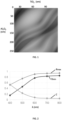
- the figure 2 shows the evolution of the contrast C for a monolayer of alumina (Al 2 O 3 ) deposited by an ALD method directly on a brass body 10 for the different wavelengths of the human visible spectrum.
- the coefficients R max and R min approach each other, and, consequently, the contrast C remains well below 1, and in particular generally below 0.5, in the human visible spectrum. It can be seen that the contrast C even tends towards 0 for the redder colors. It emerges from this limitation that the colors achievable by such an alumina-based transmission layer 30 on a brass body 10 are mainly shades of yellow and this with a very high luminance.
- the reflection coefficients R at the interfaces in such an interference optical system 40 comprising the above-mentioned transmission layers 30 are relatively low, typically less than 20%.
- the reflection coefficient at an air - TiO 2 interface is about 18%, about 6% at an air - Al 2 O 3 interface and about 4% at a TiO 2 - Al 2 O 3 interface.
- the reflection coefficient R 2 at the interface between the transmission layer(s) 30 and the body 10 of the component 1 must also be similarly relatively low, which may in particular be the case if the refraction indices n 0 and n 1 are close and the value of k 1 is relatively low.
- the interference optical system 40 comprises, under the transmission layer(s) 30, an absorption layer 20 whose complex refractive index coefficients allow the interference optical system 40 to obtain a high interference contrast C on the human visible spectrum. More precisely, it is sought that the absorption layer 20 forms a reflection coefficient R 2 at the interface between the absorption layer 20 and the transmission layer 30 as close as possible to that R 1 at the interface between the transmission layer 30 and the air surrounding the watch component 1 on the human visible spectrum.
- the contrast C typically has a preferred value of high contrast, i.e. at least equal to 0.7.
- the reflection coefficient R 1 at an air - TiO 2 interface evolving between approximately 27% and 17% on the human visible spectrum by having a value of approximately 18% at the wavelength of 550 nm the reflection coefficient R 2 at a TiO 2 - absorption layer 20 interface should preferentially evolve between approximately 43% - 11% and 33% - 1% on the human visible spectrum.
- the reflection value R 2 when it reaches 1.2% is at a limit below which it becomes difficult to find a material that can satisfy this characteristic.
- the reflection coefficient R 1 at an air - Al 2 O 3 interface evolving between approximately 6.5% and 5.5% on the human visible spectrum, we understand that it will be more frequent to find materials allowing to obtain a reflection coefficient R 2 at the interface higher than that R 1 of the air - Al 2 O 3 interface.
- the absorption layer 20 is therefore not intended to reflect the maximum amount of light transmitted by the transmission layer(s) 30 but to adapt the reflection of this transmitted light in order to limit the luminance, i.e. to selectively absorb and reflect the incident light in the interference optical system 40 to enable a wide variety of colours to be obtained by the nature and thickness of each transmission layer 30 deposited against the absorption layer 20. It is therefore possible to obtain colours having colour space parameters, such as for example CIELAB, with more precise values so that the difference between the desired target and the colour obtained is minimised and reproducible.
- colour space parameters such as for example CIELAB
- the interference optical system 40 thus makes it possible to change the visual appearance of a component, that is to say in particular its color. Indeed, the combination of the absorption layer 20 under the transmission layer 30 allows the interference optical system 40 to offer a very precise color shade among a wide variety of possible colors. More precisely, the interference optical system 40 according to the invention makes it possible to selectively modulate the intensity of reflected light to offer, relatively constantly over the entire human visible spectrum, a high interference visibility, or high interference contrast C, that is to say at least equal to 0.7, preferably at least equal to 0.75 and ideally as close as possible to the optimal value of 1.
- the absorption layer 20 preferably has a thickness at least equal to 50 nm, and more preferably a thickness at least equal to 100 nm, so that the electromagnetic wave associated with the incident light cannot or can barely reach the body 10 of the component 1 below the absorption layer 20.
- the absorption layer 20 can thus have a thickness equal to 50 nm, 60 nm, 70 nm, 80 nm, 90 nm, 100 nm, 110 nm, 120 nm, 130 nm, 140 nm, 150 nm, 160 nm, 170 nm, 180 nm, 190 nm, 200 nm, 225 nm or 250 nm.
- incident light is blocked from reaching the body 10 of the component 1 or is absorbed when reflected at the interface between the body 10 of the component 1 and the absorption layer 20.
- An absorption layer 20 with a thickness of 200 nm has been found to be satisfactory.
- This absorption layer 20 may be deposited by various means, but preferably it is formed by electrodeposition such as electroplating.
- the absorption layer 20 may also be deposited by an autocatalytic deposition process or a physical or chemical vapor deposition process.
- a ceramic transmission layer 30 such as, for example, based on an oxide preferably metallic, of a preferably metallic carbide, of a preferably metallic sulfide or of a preferably metallic nitride
- the inventors found that a nickel-based or zinc-based absorption layer 20 gave full satisfaction, in particular because these layers had complex refractive indices making it possible to obtain a high contrast C.
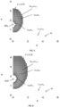
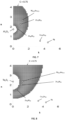
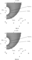
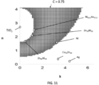
- Figures 5 to 11 indicate, each for a single type of transmission layer 30 material, the location of different absorption layer 20 materials relative to a preferred high contrast zone C.
- figure 5 illustrates a high contrast region C for an interference optical system 40 with a single silicon oxide (SiO 2 ) transmission layer 30 relative to the real and imaginary parts of the refractive index of different absorption layer 20 materials.
- figure 6 illustrates a high contrast region C for an interference optical system 40 with a single zinc oxide (ZnO) transmission layer 30 relative to the real and imaginary parts of the refractive index of different absorption layer 20 materials.
- SiO 2 silicon oxide
- ZnO zinc oxide
- figure 7 illustrates a high contrast region C for an interference optical system 40 with a single transmitting layer 30 of alumina (Al 2 O 3 ) relative to the real and imaginary parts of the refractive index of different absorption layer 20 materials.
- figure 8 illustrates a high contrast region C for an interference optical system 40 with a single transmission layer 30 of tantalum oxide (Ta 2 O 5 ) relative to the real and imaginary parts of the refractive index of different absorption layer 20 materials.
- figure 9 illustrates a high contrast region C for an interference optical system 40 with a single transmitting layer 30 of zirconia (ZrO 2 ) relative to the real and imaginary parts of the refractive index of different absorption layer 20 materials.
- ZrO 2 zirconia
- figure 10 illustrates a high contrast region C for an interference optical system 40 with a single transmission layer 30 of hafnium oxide (HfO 2 ) relative to the real and imaginary parts of the refractive index of different absorption layer 20 materials.
- figure 11 illustrates a high contrast region C for an interference optical system 40 with a single transmitting layer 30 of titanium oxide (TiO 2 ) relative to the real and imaginary parts of the refractive index of different absorption layer 20 materials.
- HfO 2 hafnium oxide
- TiO 2 titanium oxide
- the high contrast area C represents an area in which the average contrast C over the human visible spectrum is at least approximately 0.75, with the contrast being higher at the center of the area than at its borders.
- the absorption layer 20 has a constant complex refractive index (n, k) over the spectral range between 340 and 780 nm
- the values of the refractive indices of the substrates indicated on the figures 5 to 11 are taken at 550 nm, which is in the middle of the 340-780 nm spectral range.
- a nickel- or zinc-based absorption layer 20 offers a reflection coefficient R 2 at the interface between the absorption layer 20 and the transmission layer 30 close to that R 1 at the interface between the transmission layer 30 and the air surrounding the watch component 1 on the human visible spectrum.
- Nickel belongs to the group of elements called transition metals in the periodic table of elements, also called the Mendeleev table, which has good light absorption properties since it can form stable ions with "d" atomic orbitals that are only partially filled.
- Mendeleev table which has good light absorption properties since it can form stable ions with "d" atomic orbitals that are only partially filled.
- nickel in pure form, i.e. containing at least 95% nickel, nickel has a silver-white color that remains colorimetrically neutral.
- zinc (Zn) in pure form, i.e. containing at least 95% zinc, zinc has a light gray color which remains neutral in terms of colorimetry.
- an absorption layer 20 may be based on a material other than nickel or zinc in order, according to the invention, to offer a reflection coefficient R 2 at the interface between the absorption layer 20 and the transmission layer 30 close to that R 1 at the interface between the transmission layer 30 and the air surrounding the watch component 1 on the human visible spectrum.
- the interference optical system 40 may comprise several transmission layers 30 stacked on top of each other over the absorption layer 20 in order to be able to select a precise color. Indeed, it is advantageously possible, by selecting the nature and thickness of each layer 30 of this stack, to modulate the intensity of reflected light in order to create a very precise shade of color on the component 1.
- the interference optical system 40 comprises at least one transmission layer 30 made of aluminum oxide (Al 2 O 3 ).
- the interference optical system 40 comprises at least one transmission layer 30 made of titanium dioxide (TiO 2 ).
- the interference optical system 40 comprises at least one transmission layer 30 made of aluminum oxide (Al 2 O 3 ) and at least one transmission layer 30 made of titanium dioxide (TiO 2 ).
- At least one first transmission layer 30, 30a, 30c, 30e is stacked on at least one second transmission layer 30, 30b, 30d with respectively different refractive indices making it possible to vary the color of the component according to the variations in nature, refractive index and thickness of each transmission layer 30. It is thus preferred to alternate a transmission layer 30, 30a, 30c, 30e with a low refractive index, i.e. for example between 1.45 and 1.95 at a wavelength of 620 nm, with another transmission layer 30, 30b, 30d with a high refractive index, i.e. for example between 2.1 and 3.0 at a wavelength of 620 nm, in order to more precisely modulate the reflected light and more easily adjust the desired color shade.
- a low refractive index i.e. for example between 1.45 and 1.95 at a wavelength of 620 nm
- another transmission layer 30, 30b, 30d with a high refractive index, i.e. for example between 2.1 and 3.0 at a wavelength of
- the interference optical system 40 comprises a stack of transmission layers 30, 30a, 30b, 30c, 30d, 30e, i.e. without the thickness of the absorption layer 20, the total thickness of which is less than 2 ⁇ m.
- the total thickness of the absorption layer 20 is less than 2 ⁇ m.
- R n B ⁇ n H 2 + k B 2 n B + n H 2 + k B 2
- k B is the extinction coefficient of the low refractive index transmission layer 30 which can be considered negligible (as can the extinction coefficient of the high refractive index transmission layer 30).
- the overall refractive index of the stack of transmission layers 30 is preferably between 1.45 and 2.7 on the human visible spectrum.
- the interference optical system 40 comprises, for this example, a transmission layer 30 made of aluminum oxide (Al 2 O 3 ) with a low refractive index on the human visible spectrum, i.e. between 1.6 and 1.7, which is deposited above a transmission layer 30 of titanium oxide (TiO 2 ) with a high refractive index on the human visible spectrum, i.e. between 2.1 and 3.0.
- Al 2 O 3 aluminum oxide
- TiO 2 titanium oxide
- the absorption layer 20 is intended to adapt the reflection coefficient at its interface with the first of the transmission layers 30 to the reflection coefficients of the other interfaces of the interference optical system 40, or even in this example of the interfaces between a “high index” transmission layer 30 with a “low index” transmission layer 30 as well as the interface of the last transmission layer 30 with the air surrounding the component 1.
- the material of the transmission layer 20 can be modified to adapt the coefficients of its complex refractive index without losing any of its other qualities.
- the absorption layer 20 can thus be an alloy comprising nickel or zinc in order to adapt its complex reflection index coefficients while maintaining great stability over the human visible spectrum.
- an absorption layer 20 based on a binary alloy comprising gold or zinc in addition to nickel or nickel in addition to zinc was satisfactory.
- alloys of the Ni-Au or Ni-Zn type, or of the Zn-Ni type are only examples and are not the only ones allowing the advantages of the invention to be obtained. It is of course possible to envisage alloys other than binary ones and, in particular, which could comprise more elements than two metals outside the usual so-called pollution compounds whose proportion by weight does not exceed 0.2% of the total mass of the alloy.
- the binary Zn-Ni alloy can be deposited by electroplating using an electrolyte bath whose base consists mainly of nickel sulfate hexahydrate 10 - 25%, nickel chloride hexahydrate 2.5 - 10%, zinc sulfate (mono-, hexa- and heptahydrate) 2.5 - 10%, sodium thiocyanate ⁇ 2.5% and an electrometric pH (at 20 °C) of 5.8 to 6.
- the deposition temperature can be adjusted in a window between 22 °C and 17 °C. Preferably, it is regulated along the deposition at 18 °C and the current density from 0.12 to 0.15 A.dm -2 .
- the resulting binary alloy comprises, for example, 60 to 80% zinc by total weight of the alloy and 20 to 40% remaining nickel.
- the alloy comprises substantially 80% zinc and 20% remaining nickel and has a dark gray color.
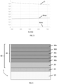
- figure 3 shows the evolution of the contrast C for a monolayer of alumina (Al 2 O 3 ) deposited on an absorption layer 20 in such a zinc-nickel alloy. It emerges from the figure 3 that the value of the contrast C remains advantageously greater than 0.8 over the entire human visible spectrum.
- the alloy of substantially 80% zinc and 20% nickel exhibits a complex refractive index at a wavelength of 550 nm with n ⁇ 1.8 and k ⁇ 0.32.
- the alloy comprises substantially 70% zinc and the remaining 30% nickel and results in an interference optical system 40 having a contrast C similar to that of substantially 80% zinc and 20% nickel across the entire human visible spectrum.
- the alloy of approximately 70% zinc and 30% nickel exhibits a complex refractive index at a wavelength of 550 nm with n ⁇ 2.1 and k ⁇ 1.2.
- the resulting binary alloy comprises, for example, 50 to 70% nickel by total weight of the alloy and the remaining 30 to 50% gold.
- the alloy comprises 60 to 65% nickel and 35 to 40% gold.
- the alloy comprises substantially 62.5% nickel and 37.5% gold, and has a gray-black color.
- the alloy of approximately 62.5% nickel and 37.5% gold exhibits a complex refractive index at a wavelength of 550 nm with n ⁇ 2.5 and k ⁇ 1.4.
- the absorption layer may comprise from 50 to 97% nickel by total weight of the alloy and from 3 to 50% remaining zinc.
- the absorption layer comprises between 80% and 90% nickel by total weight of the alloy and between 10% and 20% remaining zinc. Alloys of this type and methods for depositing them by electroplating are described for example in the document US 4,416,737 .
- the high contrast C is obtained for a real part n of the refractive index of the nickel-based or zinc-based absorption layer 20 at a wavelength of 550 nm advantageously greater than or equal to 1.25, and preferably greater than or equal to 1.5 and even more preferably greater than or equal to 1.75, and/or an imaginary part k of the refractive index of the absorption layer 20 at a wavelength of 550 nm advantageously less than or equal to 3.5, and preferably less than or equal to 2.0, and even more preferably less than or equal to 1.5.
- These values differ from the typical n and k values of other metallic materials such as brass and silver which very often have a real part n value less than 1.0 and an imaginary part k value greater than 3.5 at a wavelength of 550 nm.
- the contrast C typically has a preferred value of high contrast, i.e. at least equal to 0.7.
- the difference (R 2 - R 1 ) between the coefficients R 2 and R 1 is comprised between ⁇ 13%, and even more preferably comprised between ⁇ 10% in order to obtain an even higher contrast in the human visible spectrum.
- the interference optical system 40 comprises a stack of five transmission layers 30a, 30b, 30c, 30d, 30e deposited by an ALD method.
- the transmission layers 30a, 30c, 30e may comprise aluminum oxide (Al 2 O 3 ) or an oxide stoichiometrically close thereto, and may be deposited using successively trimethylaluminum C 6 H 18 Al 2 (TMA) and deionized water with low conductivity (for example below 1 ⁇ S.cm -1 ) as precursors in an ALD reactor, preferably at temperatures below 200 °C.
- TMA trimethylaluminum C 6 H 18 Al 2
- deionized water with low conductivity for example below 1 ⁇ S.cm -1
- the transfer of precursors into the chamber is ensured by a continuous flow of dinitrogen (N 2 ).
- the injection time for the precursors may be from 0.1 to 0.5 seconds, these injection steps being separated by purge steps with nitrogen which last from 5 to 30 seconds.
- the transmission layers 30b, 30d may comprise titanium oxide (TiO 2 ) or an oxide stoichiometrically close thereto. They may be deposited using tetrakis(dimethylamino)titanium also known as TDMAT (Ti(NMe 2 ) 4 ) or titanium tetrachloride (TiCl4) and low conductivity deionized water as precursors in an ALD reactor at conditions similar to those for layers 30a, 30c, 30e.
- TiO 2 titanium oxide
- TDMAT Ti(NMe 2 ) 4
- TiCl4 titanium tetrachloride
- the number of cycles of self-saturated growth is of course chosen according to the desired thickness.
- At least one adhesion layer 25 may be deposited between the absorption layer 20 and the body 10 of the component 1 to facilitate the mounting of the interference optical system 40 on the body 10.
- Each layer 25, for example based on pure nickel or pure gold, may thus play the role of a bonding element to avoid in particular delamination between the absorption layer 20 on the body 10.
- adhesion layer 25 the surface of the body 10 of the component 1 may be cleaned or prepared in another way before any deposition to facilitate its bonding.
Landscapes
- Physics & Mathematics (AREA)
- General Physics & Mathematics (AREA)
- Engineering & Computer Science (AREA)
- Optics & Photonics (AREA)
- Plasma & Fusion (AREA)
- Optical Filters (AREA)
Claims (15)
- Uhrenkomponente (1), die aus einem Körper (10) auf der Basis eines zu verzierenden Materials gebildet ist, der zumindest teilweise mit mindestens einem optischen Interferenzsystem (40) bedeckt ist, wobei das letztere mindestens eine Transmissionsschicht (30) aufweist, die auf der Basis eines Oxids, eines Karbids, eines Sulfids oder eines Nitrids besteht, die durch ein ALD-Verfahren erhalten wird, um zumindest teilweise Umgebungslicht durchzulassen, um das visuelle Erscheinungsbild der Uhrenkomponente (1) zu verändern, dadurch gekennzeichnet, dass das optische Interferenzsystem (40) außerdem eine Absorptionsschicht (20) auf Nickelbasis aufweist, die unter der Transmissionsschicht (30) angebracht ist, wodurch die Genauigkeit der durch das optische Interferenzsystem (40) erhaltenen Farben verbessert werden kann.
- Uhrenkomponente (1) nach dem vorhergehenden Anspruch, wobei die Absorptionsschicht (20) eine Legierung ist, die mindestens 50 % Nickel, bezogen auf das Gesamtgewicht der Legierung, enthält.
- Uhrenkomponente (1) nach dem vorhergehenden Anspruch, wobei die Absorptionsschicht (20) eine binäre Legierung ist, die neben Nickel auch Gold enthält.
- Uhrenkomponente (1) nach dem vorhergehenden Anspruch, wobei die Absorptionsschicht (20) 50 bis 70 % Nickel, bezogen auf das Gesamtgewicht der Legierung, und restliche 30 bis 50 % Gold aufweist.
- Uhrenkomponente (1) nach Anspruch 2, wobei die Absorptionsschicht (20) eine binäre Legierung ist, die neben Nickel auch Zink enthält.
- Uhrenkomponente (1) nach dem vorhergehenden Anspruch, wobei die Absorptionsschicht (20) 50 bis 97 % Nickel, bezogen auf das Gesamtgewicht der Legierung, und restliche 3 bis 50 % Zink aufweist.
- Uhrenkomponente (1) nach einem der vorhergehenden Ansprüche, wobei die Absorptionsschicht (20) eine Dicke von mindestens 50 nm, vorzugsweise von mindestens 100 nm, aufweist.
- Uhrenkomponente (1) nach einem der vorhergehenden Ansprüche, wobei das optische Interferenzsystem (40) mehrere Transmissionsschichten (30) aufweist, die über der Absorptionsschicht (20) übereinandergestapelt sind, um eine bestimmte Farbe auswählen zu können.
- Uhrenkomponente (1) nach dem vorhergehenden Anspruch, bei der mindestens eine erste Transmissionsschicht (30) auf mindestens eine zweite Transmissionsschicht (30) mit jeweils unterschiedlichen Brechungsindizes gestapelt ist, die es ermöglichen, die Farbe der Uhrenkomponente (1) zu variieren.
- Uhrenkomponente (1) nach einem der vorhergehenden Ansprüche, wobei das Material des zu verzierenden Körpers (10) auf Metall, Glas, Silizium, Polymer oder einer Kombination dieser Materialien basiert.
- Verfahren zur Herstellung einer Uhrenkomponente (1) nach einem der vorhergehenden Ansprüche, dadurch gekennzeichnet, dass das Verfahren die folgenden Schritte umfasst:- Bilden eines Körpers (10);- Aufbringen, auf mindestens einem Teil des Körpers (10), einer Absorptionsschicht (20) auf Nickelbasis;- Abscheiden, mittels eines ALD-Verfahrens, mindestens einer Transmissionsschicht (30) auf der Absorptionsschicht (20), wobei jede Transmissionsschicht (30) auf der Basis eines Oxids, Karbids, Sulfids oder Nitrids gebildet wird, um ein optisches Interferenzsystem (40) auf dem Körper (10) zu bilden.
- Verfahren nach dem vorhergehenden Anspruch, bei dem der Körper (10) aus Metall, Glas, Silizium, Polymer oder einer Kombination dieser Materialien gebildet wird.
- Verfahren nach Anspruch 11 oder 12, das zwischen dem Schritt der Bildung des Körpers (10) und dem Schritt des Aufbringens der Absorptionsschicht (20) einen Schritt des Aufbringens von mindestens einer Haftschicht (25) umfasst, um die Montage der optischen Interferenzsysteme (40) auf dem Körper (10) zu erleichtern.
- Verfahren nach einem der Ansprüche 11 bis 13, wobei der Schritt des Abscheidens der Absorptionsschicht (20) durch Elektroabscheidung, durch ein autokatalytisches Abscheidungsverfahren, durch ein physikalisches Dampfphasenabscheidungsverfahren oder durch ein chemisches Dampfphasenabscheidungsverfahren durchgeführt wird.
- Verfahren nach einem der Ansprüche 11 bis 14, bei dem der Schritt des Aufbringens nach derALD-Methode mindestens eine erste Transmissionsschicht (30) bildet, die auf mindestens eine zweite Transmissionsschicht (30) mit jeweils unterschiedlichen Brechungsindizes gestapelt ist, wodurch die Farbe der Uhrenkomponente (1) variiert werden kann.
Applications Claiming Priority (1)
| Application Number | Priority Date | Filing Date | Title |
|---|---|---|---|
| FR2003854 | 2020-04-16 |
Publications (2)
| Publication Number | Publication Date |
|---|---|
| EP3896191A1 EP3896191A1 (de) | 2021-10-20 |
| EP3896191B1 true EP3896191B1 (de) | 2025-01-08 |
Family
ID=72356060
Family Applications (1)
| Application Number | Title | Priority Date | Filing Date |
|---|---|---|---|
| EP21167737.2A Active EP3896191B1 (de) | 2020-04-16 | 2021-04-09 | Uhrenkomponente mit einem verbesserten optischen interferenzsystem, die eine schicht auf nickelbasis umfasst |
Country Status (1)
| Country | Link |
|---|---|
| EP (1) | EP3896191B1 (de) |
Families Citing this family (5)
| Publication number | Priority date | Publication date | Assignee | Title |
|---|---|---|---|---|
| EP4001458B1 (de) | 2020-11-17 | 2024-10-16 | The Swatch Group Research and Development Ltd | Verfahren zum aufbringen einer beschichtung auf ein uhrwerkbauteil und nach diesem verfahren beschichtetes uhrwerkbauteil |
| JP7852338B2 (ja) * | 2022-03-29 | 2026-04-28 | セイコーエプソン株式会社 | 時計用部品、時計、および、時計用部品の製造方法 |
| JP2024101620A (ja) * | 2023-01-18 | 2024-07-30 | セイコーエプソン株式会社 | 時計用文字板および時計 |
| CH720899A1 (fr) * | 2023-06-28 | 2025-01-15 | Richemont Int Sa | Procédé de retrait d'une couche de matériau céramique |
| FI20245549A1 (en) * | 2024-05-02 | 2025-11-03 | Picosun Oy | Coating film with a light-modulating function, related manufacturing method and coated items |
Citations (3)
| Publication number | Priority date | Publication date | Assignee | Title |
|---|---|---|---|---|
| CH709669A1 (fr) | 2014-05-19 | 2015-11-30 | Positive Coating Sa | Couche protectrice, décorative et procédé de déposition. |
| EP3896193A1 (de) | 2020-04-16 | 2021-10-20 | Richemont International S.A. | Uhrenkomponente mit einem verbesserten optischen interferenzsystem |
| EP3896192A1 (de) | 2020-04-16 | 2021-10-20 | Richemont International S.A. | Uhrenkomponente mit einem verbesserten optischen interferenzsystem, die eine schicht auf zinkbasis umfasst |
Family Cites Families (5)
| Publication number | Priority date | Publication date | Assignee | Title |
|---|---|---|---|---|
| US4416737A (en) | 1982-02-11 | 1983-11-22 | National Steel Corporation | Process of electroplating a nickel-zinc alloy on steel strip |
| EP0430874A1 (de) * | 1989-11-22 | 1991-06-05 | Balzers Aktiengesellschaft | Gegenstand mit einer Dekorschicht |
| CH703254A1 (fr) * | 2010-06-04 | 2011-12-15 | Positive Coating Sa | Article décoratif avec revêtement rouge et procédé. |
| CN102899610A (zh) | 2011-07-29 | 2013-01-30 | 鸿富锦精密工业(深圳)有限公司 | 镀膜件及其制造方法 |
| CH711122B1 (fr) | 2015-05-26 | 2019-07-15 | Estoppey Addor Sa | Composant d'une pièce d'horlogerie, article décoratif et procédé de déposition. |
-
2021
- 2021-04-09 EP EP21167737.2A patent/EP3896191B1/de active Active
Patent Citations (3)
| Publication number | Priority date | Publication date | Assignee | Title |
|---|---|---|---|---|
| CH709669A1 (fr) | 2014-05-19 | 2015-11-30 | Positive Coating Sa | Couche protectrice, décorative et procédé de déposition. |
| EP3896193A1 (de) | 2020-04-16 | 2021-10-20 | Richemont International S.A. | Uhrenkomponente mit einem verbesserten optischen interferenzsystem |
| EP3896192A1 (de) | 2020-04-16 | 2021-10-20 | Richemont International S.A. | Uhrenkomponente mit einem verbesserten optischen interferenzsystem, die eine schicht auf zinkbasis umfasst |
Non-Patent Citations (56)
Also Published As
| Publication number | Publication date |
|---|---|
| EP3896191A1 (de) | 2021-10-20 |
Similar Documents
| Publication | Publication Date | Title |
|---|---|---|
| EP3896192A1 (de) | Uhrenkomponente mit einem verbesserten optischen interferenzsystem, die eine schicht auf zinkbasis umfasst | |
| EP3896193A1 (de) | Uhrenkomponente mit einem verbesserten optischen interferenzsystem | |
| EP3896191A1 (de) | Uhrenkomponente mit einem verbesserten optischen interferenzsystem, die eine schicht auf nickelbasis umfasst | |
| EP3339983B1 (de) | Perlmuttsubstrat, das mit einer gelben schicht beschichtet ist | |
| EP4001458B1 (de) | Verfahren zum aufbringen einer beschichtung auf ein uhrwerkbauteil und nach diesem verfahren beschichtetes uhrwerkbauteil | |
| EP2717103B1 (de) | Leuchtende Spiralfeder | |
| EP2369633A2 (de) | Lichtdurchlässiges Substrat mit einer Elektrode | |
| CH709669A1 (fr) | Couche protectrice, décorative et procédé de déposition. | |
| EP4733861A2 (de) | Uhrelement | |
| FR3021414A1 (fr) | Miroir colore | |
| EP3696151A1 (de) | Farbiges armbanduhrenglas | |
| EP2274648B1 (de) | Brillenglas und herstellungsverfahren dafür | |
| EP3892151A1 (de) | Uhrenkomponente und verfahren zur herstellung einer uhrenkomponente | |
| EP3776022B1 (de) | Farbiger spiegel | |
| EP4182278A1 (de) | Emissionsarmes material mit einer beschichtung mit einem oxidationsgradienten auf titanoxidbasis | |
| CH718071A2 (fr) | Procédé de dépôt d'un revêtement sur un article, tel qu'un composant horloger et article revêtu par un tel procédé. | |
| WO2021094695A1 (fr) | Vitrage antisolaire a faible reflexion interne | |
| EP4726478A1 (de) | Schwarze dekorative dünne tialc beschichtung | |
| EP4455798B1 (de) | Verkleidungsteil aus keramischem material mit einer schutzschicht und verfahren zur herstellung eines solchen verkleidungsteils | |
| EP4640916A1 (de) | Beschichtung für ein substrat, substrat und artikel | |
| WO2020234347A1 (fr) | Miroir colore | |
| CH720742A2 (fr) | Pièce d'habillage en matériau céramique comprenant un revêtement de protection et procédé de réalisation d'une telle pièce d'habillage | |
| EP4720363A1 (de) | Farbige uhrenkomponente | |
| CH720559A2 (fr) | Procédé de fabrication d'un cadran horloger à base de polymère | |
| EP4492158A1 (de) | Verfahren zur verbesserten abscheidung von keramik |
Legal Events
| Date | Code | Title | Description |
|---|---|---|---|
| PUAI | Public reference made under article 153(3) epc to a published international application that has entered the european phase |
Free format text: ORIGINAL CODE: 0009012 |
|
| STAA | Information on the status of an ep patent application or granted ep patent |
Free format text: STATUS: THE APPLICATION HAS BEEN PUBLISHED |
|
| AK | Designated contracting states |
Kind code of ref document: A1 Designated state(s): AL AT BE BG CH CY CZ DE DK EE ES FI FR GB GR HR HU IE IS IT LI LT LU LV MC MK MT NL NO PL PT RO RS SE SI SK SM TR |
|
| B565 | Issuance of search results under rule 164(2) epc |
Effective date: 20210811 |
|
| STAA | Information on the status of an ep patent application or granted ep patent |
Free format text: STATUS: REQUEST FOR EXAMINATION WAS MADE |
|
| 17P | Request for examination filed |
Effective date: 20220411 |
|
| RBV | Designated contracting states (corrected) |
Designated state(s): AL AT BE BG CH CY CZ DE DK EE ES FI FR GB GR HR HU IE IS IT LI LT LU LV MC MK MT NL NO PL PT RO RS SE SI SK SM TR |
|
| STAA | Information on the status of an ep patent application or granted ep patent |
Free format text: STATUS: EXAMINATION IS IN PROGRESS |
|
| 17Q | First examination report despatched |
Effective date: 20230202 |
|
| GRAP | Despatch of communication of intention to grant a patent |
Free format text: ORIGINAL CODE: EPIDOSNIGR1 |
|
| STAA | Information on the status of an ep patent application or granted ep patent |
Free format text: STATUS: GRANT OF PATENT IS INTENDED |
|
| INTG | Intention to grant announced |
Effective date: 20241014 |
|
| GRAS | Grant fee paid |
Free format text: ORIGINAL CODE: EPIDOSNIGR3 |
|
| GRAA | (expected) grant |
Free format text: ORIGINAL CODE: 0009210 |
|
| STAA | Information on the status of an ep patent application or granted ep patent |
Free format text: STATUS: THE PATENT HAS BEEN GRANTED |
|
| AK | Designated contracting states |
Kind code of ref document: B1 Designated state(s): AL AT BE BG CH CY CZ DE DK EE ES FI FR GB GR HR HU IE IS IT LI LT LU LV MC MK MT NL NO PL PT RO RS SE SI SK SM TR |
|
| REG | Reference to a national code |
Ref country code: GB Ref legal event code: FG4D Free format text: NOT ENGLISH |
|
| REG | Reference to a national code |
Ref country code: CH Ref legal event code: EP |
|
| REG | Reference to a national code |
Ref country code: DE Ref legal event code: R096 Ref document number: 602021024559 Country of ref document: DE |
|
| REG | Reference to a national code |
Ref country code: IE Ref legal event code: FG4D Free format text: LANGUAGE OF EP DOCUMENT: FRENCH |
|
| REG | Reference to a national code |
Ref country code: LT Ref legal event code: MG9D |
|
| REG | Reference to a national code |
Ref country code: NL Ref legal event code: MP Effective date: 20250108 |
|
| REG | Reference to a national code |
Ref country code: AT Ref legal event code: MK05 Ref document number: 1758372 Country of ref document: AT Kind code of ref document: T Effective date: 20250108 |
|
| PG25 | Lapsed in a contracting state [announced via postgrant information from national office to epo] |
Ref country code: NL Free format text: LAPSE BECAUSE OF FAILURE TO SUBMIT A TRANSLATION OF THE DESCRIPTION OR TO PAY THE FEE WITHIN THE PRESCRIBED TIME-LIMIT Effective date: 20250108 |
|
| PG25 | Lapsed in a contracting state [announced via postgrant information from national office to epo] |
Ref country code: RS Free format text: LAPSE BECAUSE OF FAILURE TO SUBMIT A TRANSLATION OF THE DESCRIPTION OR TO PAY THE FEE WITHIN THE PRESCRIBED TIME-LIMIT Effective date: 20250408 |
|
| PG25 | Lapsed in a contracting state [announced via postgrant information from national office to epo] |
Ref country code: FI Free format text: LAPSE BECAUSE OF FAILURE TO SUBMIT A TRANSLATION OF THE DESCRIPTION OR TO PAY THE FEE WITHIN THE PRESCRIBED TIME-LIMIT Effective date: 20250108 |
|
| PG25 | Lapsed in a contracting state [announced via postgrant information from national office to epo] |
Ref country code: PL Free format text: LAPSE BECAUSE OF FAILURE TO SUBMIT A TRANSLATION OF THE DESCRIPTION OR TO PAY THE FEE WITHIN THE PRESCRIBED TIME-LIMIT Effective date: 20250108 |
|
| PG25 | Lapsed in a contracting state [announced via postgrant information from national office to epo] |
Ref country code: ES Free format text: LAPSE BECAUSE OF FAILURE TO SUBMIT A TRANSLATION OF THE DESCRIPTION OR TO PAY THE FEE WITHIN THE PRESCRIBED TIME-LIMIT Effective date: 20250108 |
|
| PG25 | Lapsed in a contracting state [announced via postgrant information from national office to epo] |
Ref country code: NO Free format text: LAPSE BECAUSE OF FAILURE TO SUBMIT A TRANSLATION OF THE DESCRIPTION OR TO PAY THE FEE WITHIN THE PRESCRIBED TIME-LIMIT Effective date: 20250408 Ref country code: IS Free format text: LAPSE BECAUSE OF FAILURE TO SUBMIT A TRANSLATION OF THE DESCRIPTION OR TO PAY THE FEE WITHIN THE PRESCRIBED TIME-LIMIT Effective date: 20250508 |
|
| PG25 | Lapsed in a contracting state [announced via postgrant information from national office to epo] |
Ref country code: HR Free format text: LAPSE BECAUSE OF FAILURE TO SUBMIT A TRANSLATION OF THE DESCRIPTION OR TO PAY THE FEE WITHIN THE PRESCRIBED TIME-LIMIT Effective date: 20250108 |
|
| PG25 | Lapsed in a contracting state [announced via postgrant information from national office to epo] |
Ref country code: PT Free format text: LAPSE BECAUSE OF FAILURE TO SUBMIT A TRANSLATION OF THE DESCRIPTION OR TO PAY THE FEE WITHIN THE PRESCRIBED TIME-LIMIT Effective date: 20250508 Ref country code: LV Free format text: LAPSE BECAUSE OF FAILURE TO SUBMIT A TRANSLATION OF THE DESCRIPTION OR TO PAY THE FEE WITHIN THE PRESCRIBED TIME-LIMIT Effective date: 20250108 |
|
| PG25 | Lapsed in a contracting state [announced via postgrant information from national office to epo] |
Ref country code: BG Free format text: LAPSE BECAUSE OF FAILURE TO SUBMIT A TRANSLATION OF THE DESCRIPTION OR TO PAY THE FEE WITHIN THE PRESCRIBED TIME-LIMIT Effective date: 20250108 Ref country code: GR Free format text: LAPSE BECAUSE OF FAILURE TO SUBMIT A TRANSLATION OF THE DESCRIPTION OR TO PAY THE FEE WITHIN THE PRESCRIBED TIME-LIMIT Effective date: 20250409 |
|
| PG25 | Lapsed in a contracting state [announced via postgrant information from national office to epo] |
Ref country code: AT Free format text: LAPSE BECAUSE OF FAILURE TO SUBMIT A TRANSLATION OF THE DESCRIPTION OR TO PAY THE FEE WITHIN THE PRESCRIBED TIME-LIMIT Effective date: 20250108 |
|
| PG25 | Lapsed in a contracting state [announced via postgrant information from national office to epo] |
Ref country code: SE Free format text: LAPSE BECAUSE OF FAILURE TO SUBMIT A TRANSLATION OF THE DESCRIPTION OR TO PAY THE FEE WITHIN THE PRESCRIBED TIME-LIMIT Effective date: 20250108 |
|
| PG25 | Lapsed in a contracting state [announced via postgrant information from national office to epo] |
Ref country code: SM Free format text: LAPSE BECAUSE OF FAILURE TO SUBMIT A TRANSLATION OF THE DESCRIPTION OR TO PAY THE FEE WITHIN THE PRESCRIBED TIME-LIMIT Effective date: 20250108 |
|
| REG | Reference to a national code |
Ref country code: DE Ref legal event code: R026 Ref document number: 602021024559 Country of ref document: DE |
|
| PG25 | Lapsed in a contracting state [announced via postgrant information from national office to epo] |
Ref country code: DK Free format text: LAPSE BECAUSE OF FAILURE TO SUBMIT A TRANSLATION OF THE DESCRIPTION OR TO PAY THE FEE WITHIN THE PRESCRIBED TIME-LIMIT Effective date: 20250108 |
|
| PLBI | Opposition filed |
Free format text: ORIGINAL CODE: 0009260 |
|
| REG | Reference to a national code |
Ref country code: CH Ref legal event code: L11 Free format text: ST27 STATUS EVENT CODE: U-0-0-L10-L11 (AS PROVIDED BY THE NATIONAL OFFICE) Effective date: 20251015 |
|
| PLAB | Opposition data, opponent's data or that of the opponent's representative modified |
Free format text: ORIGINAL CODE: 0009299OPPO |
|
| PG25 | Lapsed in a contracting state [announced via postgrant information from national office to epo] |
Ref country code: CZ Free format text: LAPSE BECAUSE OF FAILURE TO SUBMIT A TRANSLATION OF THE DESCRIPTION OR TO PAY THE FEE WITHIN THE PRESCRIBED TIME-LIMIT Effective date: 20250108 Ref country code: EE Free format text: LAPSE BECAUSE OF FAILURE TO SUBMIT A TRANSLATION OF THE DESCRIPTION OR TO PAY THE FEE WITHIN THE PRESCRIBED TIME-LIMIT Effective date: 20250108 |
|
| PLAX | Notice of opposition and request to file observation + time limit sent |
Free format text: ORIGINAL CODE: EPIDOSNOBS2 |
|
| REG | Reference to a national code |
Ref country code: CH Ref legal event code: L10 Free format text: ST27 STATUS EVENT CODE: U-0-0-L10-L00 (AS PROVIDED BY THE NATIONAL OFFICE) Effective date: 20251022 |
|
| PG25 | Lapsed in a contracting state [announced via postgrant information from national office to epo] |
Ref country code: RO Free format text: LAPSE BECAUSE OF FAILURE TO SUBMIT A TRANSLATION OF THE DESCRIPTION OR TO PAY THE FEE WITHIN THE PRESCRIBED TIME-LIMIT Effective date: 20250108 |
|
| PG25 | Lapsed in a contracting state [announced via postgrant information from national office to epo] |
Ref country code: SK Free format text: LAPSE BECAUSE OF FAILURE TO SUBMIT A TRANSLATION OF THE DESCRIPTION OR TO PAY THE FEE WITHIN THE PRESCRIBED TIME-LIMIT Effective date: 20250108 |
|
| 26 | Opposition filed |
Opponent name: ICB INGENIEURS CONSEILS EN BREVETS SA Effective date: 20251008 |
|
| R26 | Opposition filed (corrected) |
Opponent name: ICB INGENIEURS CONSEILS EN BREVETS SA Effective date: 20251008 |
|
| PLAB | Opposition data, opponent's data or that of the opponent's representative modified |
Free format text: ORIGINAL CODE: 0009299OPPO |
|
| REG | Reference to a national code |
Ref country code: CH Ref legal event code: L10 Free format text: ST27 STATUS EVENT CODE: U-0-0-L10-L00 (AS PROVIDED BY THE NATIONAL OFFICE) Effective date: 20251210 |
|
| PG25 | Lapsed in a contracting state [announced via postgrant information from national office to epo] |
Ref country code: LU Free format text: LAPSE BECAUSE OF NON-PAYMENT OF DUE FEES Effective date: 20250409 |
|
| PG25 | Lapsed in a contracting state [announced via postgrant information from national office to epo] |
Ref country code: MC Free format text: LAPSE BECAUSE OF FAILURE TO SUBMIT A TRANSLATION OF THE DESCRIPTION OR TO PAY THE FEE WITHIN THE PRESCRIBED TIME-LIMIT Effective date: 20250108 |
|
| REG | Reference to a national code |
Ref country code: BE Ref legal event code: MM Effective date: 20250430 |
|
| R26 | Opposition filed (corrected) |
Opponent name: ICB INGENIEURS CONSEILS EN BREVETS SA Effective date: 20251008 |
|
| PG25 | Lapsed in a contracting state [announced via postgrant information from national office to epo] |
Ref country code: BE Free format text: LAPSE BECAUSE OF NON-PAYMENT OF DUE FEES Effective date: 20250430 |
|
| PG25 | Lapsed in a contracting state [announced via postgrant information from national office to epo] |
Ref country code: IT Free format text: LAPSE BECAUSE OF FAILURE TO SUBMIT A TRANSLATION OF THE DESCRIPTION OR TO PAY THE FEE WITHIN THE PRESCRIBED TIME-LIMIT Effective date: 20250108 |
|
| PLBB | Reply of patent proprietor to notice(s) of opposition received |
Free format text: ORIGINAL CODE: EPIDOSNOBS3 |
|
| PG25 | Lapsed in a contracting state [announced via postgrant information from national office to epo] |
Ref country code: IE Free format text: LAPSE BECAUSE OF NON-PAYMENT OF DUE FEES Effective date: 20250409 |
|
| REG | Reference to a national code |
Ref country code: CH Ref legal event code: U11 Free format text: ST27 STATUS EVENT CODE: U-0-0-U10-U11 (AS PROVIDED BY THE NATIONAL OFFICE) Effective date: 20260501 |
|
| PG25 | Lapsed in a contracting state [announced via postgrant information from national office to epo] |
Ref country code: CY Free format text: LAPSE BECAUSE OF FAILURE TO SUBMIT A TRANSLATION OF THE DESCRIPTION OR TO PAY THE FEE WITHIN THE PRESCRIBED TIME-LIMIT Effective date: 20250108 |
|
| PG25 | Lapsed in a contracting state [announced via postgrant information from national office to epo] |
Ref country code: LT Free format text: LAPSE BECAUSE OF FAILURE TO SUBMIT A TRANSLATION OF THE DESCRIPTION OR TO PAY THE FEE WITHIN THE PRESCRIBED TIME-LIMIT Effective date: 20250108 |
|
| PGFP | Annual fee paid to national office [announced via postgrant information from national office to epo] |
Ref country code: GB Payment date: 20260424 Year of fee payment: 6 |
|
| PGFP | Annual fee paid to national office [announced via postgrant information from national office to epo] |
Ref country code: DE Payment date: 20260422 Year of fee payment: 6 |
|
| PGFP | Annual fee paid to national office [announced via postgrant information from national office to epo] |
Ref country code: CH Payment date: 20260501 Year of fee payment: 6 |
|
| PGFP | Annual fee paid to national office [announced via postgrant information from national office to epo] |
Ref country code: FR Payment date: 20260420 Year of fee payment: 6 |