EP3896385A1 - Capteur de capacité électrostatique - Google Patents
Capteur de capacité électrostatique Download PDFInfo
- Publication number
- EP3896385A1 EP3896385A1 EP19895439.8A EP19895439A EP3896385A1 EP 3896385 A1 EP3896385 A1 EP 3896385A1 EP 19895439 A EP19895439 A EP 19895439A EP 3896385 A1 EP3896385 A1 EP 3896385A1
- Authority
- EP
- European Patent Office
- Prior art keywords
- electrostatic capacitance
- wafer
- detection unit
- differential amplifier
- wafer transfer
- Prior art date
- Legal status (The legal status is an assumption and is not a legal conclusion. Google has not performed a legal analysis and makes no representation as to the accuracy of the status listed.)
- Granted
Links
Images


Classifications
-
- H—ELECTRICITY
- H10—SEMICONDUCTOR DEVICES; ELECTRIC SOLID-STATE DEVICES NOT OTHERWISE PROVIDED FOR
- H10P—GENERIC PROCESSES OR APPARATUS FOR THE MANUFACTURE OR TREATMENT OF DEVICES COVERED BY CLASS H10
- H10P72/00—Handling or holding of wafers, substrates or devices during manufacture or treatment thereof
- H10P72/06—Apparatus for monitoring, sorting, marking, testing or measuring
- H10P72/0606—Position monitoring, e.g. misposition detection or presence detection
- H10P72/0608—Position monitoring, e.g. misposition detection or presence detection of substrates stored in a container, a magazine, a carrier, a boat or the like
-
- B—PERFORMING OPERATIONS; TRANSPORTING
- B25—HAND TOOLS; PORTABLE POWER-DRIVEN TOOLS; MANIPULATORS
- B25J—MANIPULATORS; CHAMBERS PROVIDED WITH MANIPULATION DEVICES
- B25J11/00—Manipulators not otherwise provided for
- B25J11/0095—Manipulators transporting wafers
-
- B—PERFORMING OPERATIONS; TRANSPORTING
- B25—HAND TOOLS; PORTABLE POWER-DRIVEN TOOLS; MANIPULATORS
- B25J—MANIPULATORS; CHAMBERS PROVIDED WITH MANIPULATION DEVICES
- B25J13/00—Controls for manipulators
- B25J13/08—Controls for manipulators by means of sensing devices, e.g. viewing or touching devices
- B25J13/086—Proximity sensors
-
- B—PERFORMING OPERATIONS; TRANSPORTING
- B25—HAND TOOLS; PORTABLE POWER-DRIVEN TOOLS; MANIPULATORS
- B25J—MANIPULATORS; CHAMBERS PROVIDED WITH MANIPULATION DEVICES
- B25J15/00—Gripping heads and other end effectors
- B25J15/0014—Gripping heads and other end effectors having fork, comb or plate shaped means for engaging the lower surface on a object to be transported
-
- B—PERFORMING OPERATIONS; TRANSPORTING
- B25—HAND TOOLS; PORTABLE POWER-DRIVEN TOOLS; MANIPULATORS
- B25J—MANIPULATORS; CHAMBERS PROVIDED WITH MANIPULATION DEVICES
- B25J15/00—Gripping heads and other end effectors
- B25J15/0052—Gripping heads and other end effectors multiple gripper units or multiple end effectors
- B25J15/0057—Gripping heads and other end effectors multiple gripper units or multiple end effectors mounted on a turret
-
- B—PERFORMING OPERATIONS; TRANSPORTING
- B25—HAND TOOLS; PORTABLE POWER-DRIVEN TOOLS; MANIPULATORS
- B25J—MANIPULATORS; CHAMBERS PROVIDED WITH MANIPULATION DEVICES
- B25J19/00—Accessories fitted to manipulators, e.g. for monitoring, for viewing; Safety devices combined with or specially adapted for use in connection with manipulators
- B25J19/02—Sensing devices
- B25J19/027—Electromagnetic sensing devices
-
- G—PHYSICS
- G01—MEASURING; TESTING
- G01B—MEASURING LENGTH, THICKNESS OR SIMILAR LINEAR DIMENSIONS; MEASURING ANGLES; MEASURING AREAS; MEASURING IRREGULARITIES OF SURFACES OR CONTOURS
- G01B7/00—Measuring arrangements characterised by the use of electric or magnetic techniques
- G01B7/003—Measuring arrangements characterised by the use of electric or magnetic techniques for measuring position, not involving coordinate determination
-
- G—PHYSICS
- G01—MEASURING; TESTING
- G01B—MEASURING LENGTH, THICKNESS OR SIMILAR LINEAR DIMENSIONS; MEASURING ANGLES; MEASURING AREAS; MEASURING IRREGULARITIES OF SURFACES OR CONTOURS
- G01B7/00—Measuring arrangements characterised by the use of electric or magnetic techniques
- G01B7/02—Measuring arrangements characterised by the use of electric or magnetic techniques for measuring length, width or thickness
- G01B7/023—Measuring arrangements characterised by the use of electric or magnetic techniques for measuring length, width or thickness for measuring distance between sensor and object
-
- G—PHYSICS
- G01—MEASURING; TESTING
- G01B—MEASURING LENGTH, THICKNESS OR SIMILAR LINEAR DIMENSIONS; MEASURING ANGLES; MEASURING AREAS; MEASURING IRREGULARITIES OF SURFACES OR CONTOURS
- G01B7/00—Measuring arrangements characterised by the use of electric or magnetic techniques
- G01B7/14—Measuring arrangements characterised by the use of electric or magnetic techniques for measuring distance or clearance between spaced objects or spaced apertures
-
- G—PHYSICS
- G01—MEASURING; TESTING
- G01R—MEASURING ELECTRIC VARIABLES; MEASURING MAGNETIC VARIABLES
- G01R1/00—Details of instruments or arrangements of the types included in groups G01R5/00 - G01R13/00 and G01R31/00
- G01R1/30—Structural combination of electric measuring instruments with basic electronic circuits, e.g. with amplifier
-
- G—PHYSICS
- G01—MEASURING; TESTING
- G01R—MEASURING ELECTRIC VARIABLES; MEASURING MAGNETIC VARIABLES
- G01R17/00—Measuring arrangements involving comparison with a reference value, e.g. bridge
- G01R17/10—AC or DC measuring bridges
- G01R17/16—AC or DC measuring bridges with discharge tubes or semiconductor devices in one or more arms of the bridge, e.g. voltmeter using a difference amplifier
-
- G—PHYSICS
- G01—MEASURING; TESTING
- G01R—MEASURING ELECTRIC VARIABLES; MEASURING MAGNETIC VARIABLES
- G01R19/00—Arrangements for measuring currents or voltages or for indicating presence or sign thereof
- G01R19/0092—Measuring current only
-
- H—ELECTRICITY
- H10—SEMICONDUCTOR DEVICES; ELECTRIC SOLID-STATE DEVICES NOT OTHERWISE PROVIDED FOR
- H10P—GENERIC PROCESSES OR APPARATUS FOR THE MANUFACTURE OR TREATMENT OF DEVICES COVERED BY CLASS H10
- H10P72/00—Handling or holding of wafers, substrates or devices during manufacture or treatment thereof
- H10P72/06—Apparatus for monitoring, sorting, marking, testing or measuring
- H10P72/0606—Position monitoring, e.g. misposition detection or presence detection
-
- H—ELECTRICITY
- H10—SEMICONDUCTOR DEVICES; ELECTRIC SOLID-STATE DEVICES NOT OTHERWISE PROVIDED FOR
- H10P—GENERIC PROCESSES OR APPARATUS FOR THE MANUFACTURE OR TREATMENT OF DEVICES COVERED BY CLASS H10
- H10P72/00—Handling or holding of wafers, substrates or devices during manufacture or treatment thereof
- H10P72/30—Handling or holding of wafers, substrates or devices during manufacture or treatment thereof for conveying, e.g. between different workstations
- H10P72/34—Handling or holding of wafers, substrates or devices during manufacture or treatment thereof for conveying, e.g. between different workstations the wafers being stored in a carrier, involving loading and unloading
- H10P72/3402—Mechanical parts of transfer devices
-
- H—ELECTRICITY
- H10—SEMICONDUCTOR DEVICES; ELECTRIC SOLID-STATE DEVICES NOT OTHERWISE PROVIDED FOR
- H10P—GENERIC PROCESSES OR APPARATUS FOR THE MANUFACTURE OR TREATMENT OF DEVICES COVERED BY CLASS H10
- H10P72/00—Handling or holding of wafers, substrates or devices during manufacture or treatment thereof
- H10P72/30—Handling or holding of wafers, substrates or devices during manufacture or treatment thereof for conveying, e.g. between different workstations
- H10P72/34—Handling or holding of wafers, substrates or devices during manufacture or treatment thereof for conveying, e.g. between different workstations the wafers being stored in a carrier, involving loading and unloading
- H10P72/3411—Handling or holding of wafers, substrates or devices during manufacture or treatment thereof for conveying, e.g. between different workstations the wafers being stored in a carrier, involving loading and unloading involving loading and unloading of wafers
-
- H—ELECTRICITY
- H10—SEMICONDUCTOR DEVICES; ELECTRIC SOLID-STATE DEVICES NOT OTHERWISE PROVIDED FOR
- H10P—GENERIC PROCESSES OR APPARATUS FOR THE MANUFACTURE OR TREATMENT OF DEVICES COVERED BY CLASS H10
- H10P72/00—Handling or holding of wafers, substrates or devices during manufacture or treatment thereof
- H10P72/70—Handling or holding of wafers, substrates or devices during manufacture or treatment thereof for supporting or gripping
- H10P72/76—Handling or holding of wafers, substrates or devices during manufacture or treatment thereof for supporting or gripping using mechanical means, e.g. clamps or pinches
- H10P72/7602—Handling or holding of wafers, substrates or devices during manufacture or treatment thereof for supporting or gripping using mechanical means, e.g. clamps or pinches the wafers being placed on a robot blade or gripped by a gripper for conveyance
-
- G—PHYSICS
- G01—MEASURING; TESTING
- G01R—MEASURING ELECTRIC VARIABLES; MEASURING MAGNETIC VARIABLES
- G01R1/00—Details of instruments or arrangements of the types included in groups G01R5/00 - G01R13/00 and G01R31/00
- G01R1/20—Modifications of basic electric elements for use in electric measuring instruments; Structural combinations of such elements with such instruments
- G01R1/203—Resistors used for electric measuring, e.g. decade resistors standards, resistors for comparators, series resistors, shunts
-
- G—PHYSICS
- G01—MEASURING; TESTING
- G01R—MEASURING ELECTRIC VARIABLES; MEASURING MAGNETIC VARIABLES
- G01R19/00—Arrangements for measuring currents or voltages or for indicating presence or sign thereof
- G01R19/0023—Measuring currents or voltages from sources with high internal resistance by means of measuring circuits with high input impedance, e.g. OP-amplifiers
-
- G—PHYSICS
- G01—MEASURING; TESTING
- G01R—MEASURING ELECTRIC VARIABLES; MEASURING MAGNETIC VARIABLES
- G01R19/00—Arrangements for measuring currents or voltages or for indicating presence or sign thereof
- G01R19/22—Arrangements for measuring currents or voltages or for indicating presence or sign thereof using conversion of AC into DC
-
- H—ELECTRICITY
- H10—SEMICONDUCTOR DEVICES; ELECTRIC SOLID-STATE DEVICES NOT OTHERWISE PROVIDED FOR
- H10P—GENERIC PROCESSES OR APPARATUS FOR THE MANUFACTURE OR TREATMENT OF DEVICES COVERED BY CLASS H10
- H10P72/00—Handling or holding of wafers, substrates or devices during manufacture or treatment thereof
- H10P72/30—Handling or holding of wafers, substrates or devices during manufacture or treatment thereof for conveying, e.g. between different workstations
- H10P72/33—Handling or holding of wafers, substrates or devices during manufacture or treatment thereof for conveying, e.g. between different workstations into and out of processing chamber
- H10P72/3308—Vertical transfer of a single workpiece
-
- H—ELECTRICITY
- H10—SEMICONDUCTOR DEVICES; ELECTRIC SOLID-STATE DEVICES NOT OTHERWISE PROVIDED FOR
- H10P—GENERIC PROCESSES OR APPARATUS FOR THE MANUFACTURE OR TREATMENT OF DEVICES COVERED BY CLASS H10
- H10P72/00—Handling or holding of wafers, substrates or devices during manufacture or treatment thereof
- H10P72/70—Handling or holding of wafers, substrates or devices during manufacture or treatment thereof for supporting or gripping
- H10P72/78—Handling or holding of wafers, substrates or devices during manufacture or treatment thereof for supporting or gripping using vacuum or suction, e.g. Bernoulli chucks
Definitions
- This invention relates to an electrostatic capacitance sensor for measuring a distance between an object to be detected and the sensor, and in particular to an electrostatic capacitance detection sensor and a detection circuit that are installed in a substrate holding hand of a substrate transfer robot for transferring thin substrates such as semiconductor wafers.
- One of the methods for accurately measuring a position of an object to be detected and a distance between a substrate holding hand and a sensor detection unit is to use an electrostatic capacitance sensor.
- This method detects an electrostatic capacitance generated between an object to be detected and a detection unit that detects the object to be detected, and measures a distance between the object to be detected and the detection unit from a detected electrostatic capacitance value.
- this electrostatic capacitance sensor attempts to measure a distance between two surfaces by emitting a weak AC that is supplied from a detection circuit of the sensor from the detection unit toward the object to be detected and by detecting changes in electrostatic capacitance that occur between a detection unit surface and an object to be detected surface.
- this electrostatic capacitance sensor has been installed in a wafer hand holding a semiconductor wafer to be used for measuring a distance between the wafer hand and the semiconductor wafer.
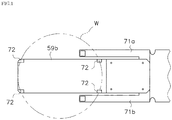
- Reference 1 describes a fork 59b mounted on a transfer apparatus for transferring a semiconductor wafer in a processing apparatus.
- Sensor heads (detection units) 71a, 71b of the electrostatic capacitance sensor are attached to left and right sides of the fork 59b, respectively. See FIG. 1 .
- the electrostatic capacitance sensor measures the electrostatic capacitance that occurs between each of the sensor heads 71a, 71b arranged on the forks 59b and the semiconductor wafer. From the measured values, it is possible to output information on the presence or absence of the semiconductor wafer, information on whether or not the semiconductor wafer and the fork 59b maintain an appropriate distance, and the like to a main controller of the transfer apparatus. Then, this main controller outputs a control signal to drive system of the transfer apparatus based on these input information, and controls the operation of the transfer apparatus.
- a threshold value is set for the electrostatic capacitance sensor, and when the fork 59b passes through the outer periphery of the semiconductor wafer, the electrostatic capacitance sensor and the drive system for driving the fork 59b operate in cooperation. Therefore, the position of the outer peripheral portion of the semiconductor wafer can be measured as an amount of movement of the fork 59b in the front-rear direction, and the position of the semiconductor wafer W in a horizontal direction can be measured by the electrostatic capacitance sensor that originally measures the distance in the vertical direction.
- Patent literature 1 Japanese Patent Laid Open Publication No. H08-335622
- the fork 59b described in the reference cannot accurately detect the semiconductor wafer.
- semiconductors have been miniaturized to a circuit line width of about 20 nanometers. With the progress of such miniaturization, adhesion of particles to the surface to be processed of a semiconductor wafer has become a major problem.
- one of causes of the particles adhering to the surface of the semiconductor wafer is charging of the semiconductor wafer.
- Semiconductor wafers are subjected to various surface treatments in each semiconductor manufacturing process. At this time, the semiconductor wafer is charged, which causes the particles to adhere to the surface of the semiconductor wafer. Further, charging of the semiconductor wafer not only attracts particles but also causes circuit patterns formed on the surface of the semiconductor wafer to be destroyed.
- a static eliminator is installed in an internal space of a semiconductor manufacturing apparatus or a wafer transfer apparatus in order to prevent the semiconductor wafer from being charged.
- the static eliminator applies a voltage of a predetermined frequency to an emitter, which is a needle-shaped electrode, and causes a corona discharge between the electrode and a ground plane to generate positive ions or negative ions. Ions generated by this static eliminator move to a charged article such as a semiconductor wafer by downward air flow supplied from an FFU (Fun Filter Unit) installed in the transfer apparatus to eliminate static electricity in the article.
- FFU Full Filter Unit
- static eliminators Since static eliminators are used while discharging by applying high voltages of several thousand to tens of thousands of volts at a predetermined frequency, they generate fluctuating electric and fluctuating magnetic fields in the surroundings. These fluctuating electric and fluctuating magnetic fields become noise and cause malfunctions in measuring instruments and electronic equipment installed in the transfer apparatus, and interfere accurate detection of an electrostatic capacitance sensor. In addition, noise due to the operation of the drive source located inside the transfer apparatus also interferes accurate detection of capacitance.
- the present invention has been made in view of the above problems, and provides an electrostatic capacitance sensor capable of stably detecting an object to be detected even in the internal space of the transfer apparatus inside which a noise generation source such as a static eliminator is located.
- the electrostatic capacitance sensor of the present invention is an electrostatic capacitance sensor that measures a distance between a detection unit and the object to be detected, and is provided with an AC supply source for supplying AC voltage to the detection unit, a parasitic capacitance compensation circuit, an operational amplifier, a differential amplifier, a phase detection means, and a low-pass filter.
- An output terminal of the operational amplifier is connected to an inverting input terminal of the differential amplifier through a first band-pass filter, the AC supply source is connected to a non-inverting input terminal of the differential amplifier through a second band-pass filter, an output terminal of the differential amplifier is connected to an input terminal of the phase detection means, and the phase detection means uses a carrier wave output from the AC supply source as a reference signal.
- the electrostatic capacitance sensor of the present invention can accurately detect even a minute change in capacitance without being affected by noise, and can accurately measure the distance between the detection unit and the object to be detected.
- a wafer transfer robot provided with the electrostatic capacitance sensor of the present invention is characterized in that the detection unit is provided on a surface of a finger which holds the semiconductor wafer. Further, the wafer transfer apparatus provided with the wafer transfer robot including the electrostatic capacitance sensor of the present invention in the internal space is loaded with at least an FFU that maintains the internal space in a clean state, a load port that loads a storage container for storing the semiconductor wafer and opens and closes a lid of the storage container, and a static eliminator that is installed near a ceiling of the wafer transfer apparatus to eliminate static electricity in the internal space. It is characterized in that a carrier frequency output from an AC supply source included in the electrostatic capacitance sensor is higher than a frequency of the power supply applied to the emitter of the static eliminator.
- the electrostatic capacitance sensor of the present invention can detect even a minute change in capacitance. Further, even if the detection unit of the electrostatic capacitance sensor of the present invention is attached to the surface of the finger of the wafer transfer robot, it does not interfere with the semiconductor wafer, and the semiconductor wafer can be transferred without trouble. In addition, since the distance between the semiconductor wafer and the finger can be accurately detected, the teaching work of the wafer transfer robot has become easier.
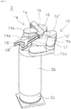
- FIG. 2 shows a wafer transfer robot 2 provided with an electrostatic capacitance sensor 1 according to the first embodiment of the present invention
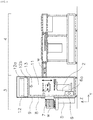
- FIGS. 3 , 4 show a wafer transfer apparatus 3 on which the wafer transfer robot 2 is mounted.
- the wafer transfer apparatus 3 of the present embodiment is called an EFEM (Equipment Front End Unit), which is an apparatus installed on a front surface of a wafer processing apparatus 4 that performs a predetermined surface treatment on a semiconductor wafer W, and is installed in a factory controlled in a clean atmosphere called a clean room together with the wafer processing apparatus 4.
- EFEM Equipment Front End Unit
- the wafer transfer apparatus 3 mainly includes a load port 5, a wafer transfer robot 2, and an X-axis table 6 for moving the wafer transfer robot 2 in the horizontal direction.
- the semiconductor wafer W being processed is stored in a state of being placed on shelf boards formed at a predetermined interval in the vertical direction inside a closed container called FOUP (Front-Opening Unified Pod) 7, and is transferred between the wafer processing apparatuses 4.
- the FOUP 7 transferred to the predetermined wafer processing apparatus 4 is set at a predetermined position of the load port 5 included in the wafer transfer apparatus 3.
- the load port 5 When the FOUP 7 is set, the load port 5 operates each drive unit to open a lid of the FOUP 7 to make the semiconductor wafer W stored inside ready for transfer.
- the semiconductor wafer W stored in the FOUP 7 is transferred to the wafer processing apparatus 4 by the wafer transfer robot 2 included in the wafer transfer apparatus 3. Further, the wafer transfer robot 2 transfers the semiconductor wafer W surface-treated by the wafer processing apparatus 4 from the wafer processing apparatus 4 to the FOUP 7.
- the load port 5 is grounded through a frame 8 of the wafer transfer apparatus 3. Further, the FOUP7 is molded of a conductive resin, and the FOUP7 mounted on the load port 5 is also grounded.
- the diameter of the semiconductor wafer W handled by the wafer transfer apparatus 3 of the present embodiment is 300 mm.
- the semiconductor wafer W is placed on the shelf board of FOUP7, and an electrostatic capacitance is generated between the shelf board and the semiconductor wafer W.
- an electrostatic capacitance is also generated between the FOUP 7 and the load port 5, and when a finger 18 of the wafer transfer robot 2 described later moves the FOUP 7 in order to transfer the semiconductor wafer W, an electrostatic capacitance is generated also between the FOUP 7 and the finger 18.
- the wafer transfer apparatus 3 includes a frame 8, a cover 9 fixed to the frame 8 in order to separate from the external atmosphere, an FFU 12 that cleans air from the outside into highly clean air and introduces it into an internal space 11 of the wafer transfer apparatus 3 as downflow, and a static eliminator 13 that supplies ionized air molecules to the internal space 11 of the wafer transfer apparatus 3 and eliminates static electricity and electrically neutralizes a charged article such as a semiconductor wafer W.
- the FFU 12 is installed on a ceiling of the wafer transfer apparatus 3, and consists of a fan 12a that sends air downward toward the internal space 11 of the wafer transfer apparatus 3 and a filter 12b that removes contaminants such as dust, organic matter present in the sent air.
- the static eliminator 13 is installed near the ceiling of the wafer transfer apparatus 3 and below the FFU 12.
- the static eliminator 13 installed in the wafer transfer apparatus 3 of the present embodiment is a corona discharge type, which electrically ionizes the surrounding air molecules by applying a high voltage supplied from an un-shown supply source to an emitter and discharging it.
- the ionized air molecules reach the surface of the semiconductor wafer W from the static eliminator 13 and electrically neutralize the charged semiconductor wafer W.
- the static eliminator 13 included in the wafer transfer apparatus 3 of the present embodiment applies a voltage of 20 Hz to the emitter to ionize surrounding air molecules.
- the frequency of the applied voltage depends on an environment in which the static eliminator 13 is located, and in the case of the wafer transfer apparatus 3, it is about 100 Hz at the maximum.
- the wafer transfer robot 2 of this embodiment includes a base 2a that is fixed to a moving part 6a of the X-axis table 6, and an elevating and rotating section 2b that can move up and down in the Z-axis direction with respect to the base 2a and that rotates on a plane (swivel plane) intersecting perpendicularly to the Z-axis direction with the central axis of the base as the rotation center.
- a pair of arm bodies 14, 15 configured symmetrically with each other are provided on an upper surface of the elevating and rotating section 2b.
- the arm bodies 14, 15 are provided with first arms 14a, 15a, second arms 14b, 15b, and wafer hands 16, 17 for holding the semiconductor wafer W, respectively.
- Base ends of the first arms 14a, 15a are rotatably attached to the elevating and rotating section 2b.
- the second arms 14b, 15b are attached to the tips of the corresponding first arms 14a, 15a, respectively, with a constant speed ratio through a belt and a pulley.
- the wafer hands 16, 17 are attached to the tips of the corresponding second arms 14b, 15b, respectively, with a constant speed ratio through a belt and a pulley.
- the arm bodies 14, 15 are configured so that rotating motion of each first arm 14a, 15a around the central axis is transmitted to each second arm 14b, 15b and each wafer hand 16, 17 with a constant speed ratio to be converted into an extending and contracting motion in a direction perpendicular to the central axis through the central axis of the wafer transfer robot 2. Therefore, the wafer transfer robot 2 can be used to transfer wafers. Therefore, the wafer transfer robot 2 has three degrees of freedom: movement (rotating movement) to rotate the elevating and rotating section 2b around the central axis, linear movement to extend and contract the arm bodies 14, 15 in forward and backward directions and Z-axis movement (elevating movement) to move the elevating and rotating section 2b in a Z-axis direction.
- the X-axis table 6 has one degree of freedom of X-axis movement (parallel movement) to move the wafer transfer robot 2 in an X-axis direction.
- the wafer transfer robot 2 can move the wafer hands 16, 17 attached to the ends of the arms to a predetermined positions in the wafer transfer apparatus 3.
- the wafer hands 16, 17 can be moved forward and backward while maintaining predetermined postures in conjunction with extending and contracting movements of the first arms and the second arms.
- Each motor which is a driving means for each of the arm bodies 14, 15, the elevating and rotating section 2b, and the X-axis table 6, has a driving shaft whose rotation angle is feedback-controlled by an unillustrated control unit included in the wafer transfer robot 2.
- control unit moves the wafer hands 16, 17 along a predetermined path taught in advance. Furthermore, the control unit is configured to receive signals from the electrostatic capacitance sensor 1 and other detection means and to correct the positions of the wafer hands 16, 17 and the wafer transfer path in accordance with a program stored in advance.
- the wafer hands 16, 17 are provided with fingers 18, 18', which are wafer holding means, respectively.
- a detection unit 1a is located on a surface of the finger 18 arranged upper to be connected to an amplifier module 1b arranged inside the finger 18.
- a detection unit 1a' is located on a surface of the finger 18' arranged below to be connected to an amplifier module 1b' arranged inside the finger 18'.
- FIG. 5 shows a finger 18 of the present embodiment.
- the finger 18 of the present embodiment is configured by airtightly bonding two plate-shaped members 18a, 18b formed in a substantially Y shape.
- the two plate-shaped members 18a, 18b are made of a light-weight and highly rigid sintered material such as alumina, and the semiconductor wafer W is placed on the top surface of the upper plate-shaped member 18a.
- a flow path 19 is formed in a substantially Y shape on the top surface of the lower plate-shaped member 18b.
- holes 21 penetrating the upper plate-shaped member 18a in the vertical direction are formed on the tips of the upper plate-shaped member 18a so as to correspond to the flow path 19.
- a hole 22 penetrating the lower plate-shaped member 18b in the vertical direction is formed on the base end portion of the lower plate-shaped member 18b so as to correspond to the flow path 19.
- the hole 22 formed in the lower plate-shaped member 18b communicates with a vacuum source (not shown) through a pipe (not shown) provided in the wafer transfer robot 2, and when the upper and lower plate-shaped members 18a, 18b are airtightly bonded, the flow path 19 forms a vacuum path, and the semiconductor wafer W placed on the finger 18 is held on the finger 18 by vacuum adsorption.
- An ellipsoidal adsorption spacer 18c is formed around the hole 21 on the top surface of the upper plate-shaped member 18a so as to surround the hole 21.
- the adsorption spacer 18c is formed in the shape of a bank raised by about 1.5 mm from the surface of the finger 18, and acts as an adsorption pad to adsorb the semiconductor wafer W.
- a support spacer 18d is formed at the center of the finger 18.
- the support spacer 18d is formed in a trapezoidal shape raised by about 1.5 mm in the same way as the adsorption spacer 18c. According to this, the semiconductor wafer W is adsorbed and supported by the adsorption spacer 18c and the support spacer 18d in a state where it floats by 1.5 mm above the finger reference surface 18e on the finger 18.
- the detection unit 1a of the electrostatic capacitance sensor 1 which is an embodiment of the present invention, is affixed to a reference surface 18e of the substantially Y-shaped finger 18.
- the electrostatic capacitance sensor 1 of this embodiment can measure a distance between the semiconductor wafer W and the fingers 18 (wafer hands 16, 17) by detecting the electrostatic capacitance between the detection unit 1a located on the fingers 18 and the semiconductor wafer W. Furthermore, it can also monitor whether or not the semiconductor wafer W is placed on the wafer hands 16, 17.
- the values detected by the detection unit 1a are transmitted to the amplifier module 1b, which is located inside the wafer hands 16, 17.
- the amplifier module 1b measures the electrostatic capacitance between the detection unit 1a and the semiconductor wafer W, and transmits the measured value to the control unit (not shown) for controlling the operation of the wafer transfer robot 2.
- the control unit converts this transmitted value into the distance between the semiconductor wafer W and the fingers 18, and reflects it in the operation of the wafer transfer robot 2.
- the detection unit 1a of the electrostatic capacitance sensor 1 in this embodiment is installed on the surface on which the semiconductor wafer W is placed of the finger 18.
- the detection unit 1a has a thickness dimension of about 0.2 mm, and has electrodes and wiring formed with conductive metal represented by copper foil on a base film of flexible material with insulation such as polyimide.
- FIG. 6 shows the detection unit 1a of this embodiment.
- the detection unit 1a of this embodiment has a structure in which guard electrode layers 24, 26, a sensor electrode layer 25, and a shield earth layer 27 are laminated.
- the first guard electrode layer 24 on which a first guard electrode 24a is formed is located on the first layer which is the top surface of the electrode layers, and the sensor electrode layer 25 on which a sensor electrode 25a is formed is located on the second layer, the second guard electrode layer 26 on which a sensor electrode 25a is formed is located on the third layer, and the shield earth layer 27 is located on the fourth layer.
- a protective film 23 is disposed on the top surface of the first guard electrode layer 24 to protect the first guard electrode layer 24.
- the detection unit 1a of this embodiment has a height dimension of about 1 mm and is used by being attached to the reference surface 18e of the finger 18.
- the adsorption spacer 18c and the support spacer 18d are formed with a height dimension of about 1.5 mm, they do not interfere with the semiconductor wafer W held by the adsorption spacer 18c and the support spacer 18d of the finger 18.
- the finger 18 included in the wafer transfer robot 2 of this embodiment is in a form of adsorbing and holding the semiconductor wafer W by vacuum pressure, the present invention is not limited thereto, and is applicable, for example, to a clamp-type finger or a Bernoulli chuck-type finger that grasps the periphery of the semiconductor wafer W.
- a sensor electrode 25a is a circular electrode for detecting the electrostatic capacitance generated between the sensor and the semiconductor wafer W, and is formed on the top surface of the base film.
- a first guard electrode 24a formed in the first guard electrode layer 24 has an inner diameter larger than the outer diameter of a sensor electrode 25a, and is formed on the top surface of the base film in an annular shape so as to surround the sensor electrode 25a.
- the sensor electrode 25a and the first guard electrode 24a are electrically insulated by the base film.
- a second guard electrode 26a formed in the second guard electrode layer 26 is formed in a circular shape having the same diameter as the outer diameter of the first guard electrode 24a formed in the first guard electrode layer 24.
- the shield earth layer 27, which is the fourth layer, is located below the second guard electrode layer 26 in which the second guard electrode 26a is formed.
- the second guard electrode 26a in this embodiment has the same diameter as the outer diameter of the first guard electrode 24a, the present invention is not limited thereto, and the diameter of the second guard electrode 26a may be formed larger than the outer diameter of the first guard electrode 24a.
- the shield earth layer 27 is an electrode made of conductive metal, such as copper foil, formed into a circular shape with the same diameter as the first and second guard electrode layers 24, 26, and is connected to a ground terminal of the wafer transfer apparatus 3 through an earth wire (not shown).
- This shield earth layer 27 prevents the influence of the electric field radiated from the guard electrodes 24a, 26a from going downward, so that the electrostatic capacitance sensor 1 is not affected by the object to be detected that exists below the detection unit 1a, and can measure only the electrostatic capacitance generated between the object to be detected above the finger 18 and the detection unit 1a.
- a linear circuit pattern 25b for electrically connecting the sensor electrode 25a and the inverting input terminal of an operational amplifier 28 of the amplifier module 1b is formed in the sensor electrode 25a included in the sensor electrode layer 25 that is the second layer.
- a linear circuit pattern 24b for electrically connecting the first guard electrode 24a and the non-inverting input terminal of the operational amplifier 28 of the amplifier module 1b is formed in the first guard electrode 24a included in the first guard electrode layer 24 that is the first layer so as to be parallel to the circuit pattern 25b connected to the sensor electrode 25a.
- a linear circuit pattern 26b for electrically connecting the second guard electrode 26a and the non-inverting input terminal of the operational amplifier 28 of the amplifier module 1b is formed in the second guard electrode 26a included in the second guard electrode layer 26 that is the third layer so as to be parallel to the circuit pattern 25b connected to the sensor electrode 25a.
- the width dimensions of the circuit patterns 24b, 26b connected to each of the guard electrodes 24a, 26a are formed so as to be thicker than the circuit pattern 25b connected to the sensor electrode 25a.
- the circuit pattern 25b connected to the sensor electrode 25a is placed so as to be sandwiched from the vertical direction by the circuit patterns 24b, 26b connected to the guard electrodes 24a, 26a, and therefore, the influence of noise on the circuit pattern 25b connected to the sensor electrode 25a is reduced.
- a protective film 23 that is an insulating layer made of the same material as the base film is arranged.
- the protective film 23 has the same external dimensions as the first layer 24 to the fourth layer 27.
- the sensor electrode formed in the detection unit 1a of the present embodiment is formed in a circular shape having a diameter of about 15 mm.
- the first guard electrode 24a is formed in a substantially annular shape having an inner diameter of about 16 mm and an outer diameter of 19 mm.
- the second guard electrode 26a is formed in a circular shape having a diameter of 20 mm.
- the external dimensions of the detection unit 1a are not limited to this embodiment, and can be appropriately changed depending on the situation.
- the electrostatic capacitance sensor 1 of the present invention is not limited to this.
- the first guard electrode 24a and the circuit pattern 24b can be formed on the top surface of the base film of the first guard electrode layer 24, and the sensor electrode 25a and the circuit pattern 25b can be formed on the opposite surface of the base film.
- the sensor electrode 25a and the circuit pattern 25b can be formed on the top surface of the base film of the sensor electrode layer 25, and the second guard electrode 26a and the circuit pattern 26b can be formed on the opposite surface of the base film.
- FIG. 7 shows a block diagram of the electrostatic capacitance sensor 1 of this embodiment.
- the sensor electrode 25a of the detection unit 1a is connected to the inverting input terminal of the operational amplifier 28 provided by the amplifier module 1b, and the guard electrodes 24a, 26a of the detection unit 1a are connected to the non-inverting input terminal of the operational amplifier 28.
- An AC voltage from an AC supply source 29 is applied to the non-inverting input terminal of the operational amplifier 28.
- the AC supply source 29 provided by the amplifier module 1b of this embodiment is configured to output a carrier wave for transmitting the electrostatic capacitance detected by the detection unit 1a at a frequency of 200 kHz with a voltage of 2 V.
- the AC supply source 29 also applies the same AC voltage to a second BPF (bandpass filter) 31 provided by the amplifier module 1b. Furthermore, the output terminal of the operational amplifier 28 is connected to a first BPF 30 provided by the amplifier module 1b. The BPFs 30, 31 will be described later.
- a feedback circuit is connected between the output terminal and the inverting input terminal of the operational amplifier 28, and a reference capacitor 32 is connected to this feedback circuit. Furthermore, the inverting input terminal of the operational amplifier 28 is provided with a parasitic capacitance compensation circuit 33 to cancel out parasitic capacitance generated in the electrodes of the detection unit 1a and the circuit of the amplifier module 1b.
- the parasitic capacitance generated inside the electrostatic capacitance sensor 1 is canceled out.
- the inverting input terminal and the non-inverting input terminal of the operational amplifier 28 are in an imaginary short circuit state, and the inverting input terminal and the non-inverting input terminal are at approximately the same potential as each other. Therefore, the sensor electrode 25a is guarded by the guard electrodes 24a, 26a.
- the output terminal of the operational amplifier 28 is connected to the inverting input terminal of a differential amplifier 34 provided by the amplifier module 1b through the first BPF 30 for passing only signals in a predetermined frequency band.
- the non-inverting input terminal of the differential amplifier 34 is also connected to the AC supply source 29 through the second BPF 31.
- Noise components generated from the semiconductor wafer W which are detected by the sensor detection unit 1a can be removed by connecting the output terminal and the non-inverting input terminal of the operational amplifier 28 to the differential amplifier 34 through the first BPF 30 and the second BPF 31.
- the noise is amplified along with the signal amplification, and a noise voltage is increased. If the noise voltage is large, the differential amplifier 34 is saturated to lose the signal. Therefore, in the amplifier module 1b of this embodiment, the noise components existing in a relatively narrow band are first removed by the first BPF 30, and then signals are amplified by the differential amplifier 34. Further, gains of the differential amplifier 34 included in the amplifier module 1b of this embodiment are set to 100 times. Therefore, saturation of the differential amplifier 34 can be prevented to proceed the signal normally.
- the amplifier module 1b of this embodiment is provided with two BPFs: one BPF 30 connected to the output terminal of the operational amplifier 28 and the other BPF 31 connected to the output terminal of the AC supply source 29.
- the signal output from the output terminal of the operational amplifier 28 is transmitted to the differential amplifier 34 with a delay with respect to the AC carrier wave output from the AC supply source 29 and the differential amplifier 34 does not amplify the difference accurately when extracting the difference between the signal output from the output terminal of the operational amplifier 28 and the AC carrier wave output from the AC supply source 29. Therefore, by allowing the carrier wave output from the AC supply source 29 to also pass through the BPF 31, the timing of the output signal from the operational amplifier 28 and the carrier wave output from the AC supply source 29 are matched.
- the delay in the signal output from the output terminal of the operational amplifier 28 can be eliminated.
- the BPFs 30, 31 included in the amplifier module 1b are set to remove frequency components other than the frequency around 200 kHz output by the AC supply source 29. According to this, low frequency noises generated by the static eliminator 13 located in the wafer transfer apparatus 3 and noises generated by the drive source of the wafer transfer robot 2 can be effectively removed.
- the inverting input terminal of the differential amplifier 34 is connected to the output terminal of the operational amplifier 28 through the BPF 30, and the non-inverting input terminal of the differential amplifier 34 is connected to the non-inverting input terminal of the operational amplifier 28 and the output terminal of the AC supply source 29 through the BPF 31.
- the signal components including the AC carrier wave from the AC supply source 29 connected to the non-inverting input terminal of the differential amplifier 34 and the electrostatic capacitance components output from the output terminal of the operational amplifier 28 to the inverting input terminal of the differential amplifier 34 through the BPF 31 are amplified to be output to a phase detection means 35.
- the phase detection means 35 included in the amplifier module 1b of this embodiment extracts the electrostatic capacitance detected by the detection unit 1a from the signal amplified by the differential amplifier 34 using the carrier wave of 2V and 200kHz output from the AC supply source 29 as a reference signal.
- the signal extracted here is output to an output terminal 37 after the noises are removed by a LPF (Low-Pass Filter) 36.
- the output terminal 37 is connected to a control unit (not shown), and the control unit calculates the distance between the finger 18 and the semiconductor wafer W from the extracted capacitance.
- the electrostatic capacitance is inversely proportional to the separation distance between the detection unit 1a and the semiconductor wafer W of the object to be detected and further the area of the detection unit 1a is known, the separation distance between the detection unit 1a and the semiconductor wafer W can be easily measured by detecting the electrostatic capacitance generated between the detection unit 1a and the semiconductor wafer W. In addition, by detecting the change in electrostatic capacitance generated between the detection unit 1a and the semiconductor wafer W, the displacement between the detection unit 1a and the semiconductor wafer W can be measured.
- the electrostatic capacitance sensor of the present invention is driven by a power supply having a relatively high frequency of about 200 kHz, so it has a configuration that can effectively remove noises of relatively low frequency components emitted from the drive source included in the static eliminator 13 and the wafer transfer robot 2, and thus, the electrostatic capacitance generated between the detection unit 1a and the object to be detected can be detected accurately.
- the detection signal amplified by the operational amplifier 28 is attenuated by the BPF 30 to remove noises and other frequency components before being amplified by the differential amplifier 34, so that the signal can be processed without saturating the differential amplifier even when large noise is introduced.
- the differential amplifier 34 and the AC supply source 29 are connected through the BPF 31 equivalent to the BPF 30 placed between the operational amplifier 28 and the differential amplifier 34, the phases of the signal from the operational amplifier 28 input to the differential amplifier 34 and the carrier wave input from the AC supply source 29 are matched. According to this, the differential amplifier 34 can perform accurate differential amplification processing and effectively attenuate noise components.
- the electrostatic capacitance sensor 1 of the present invention is provided with the amplifier module 1b capable of performing signal extraction processing with high noise tolerance, the capacitance between the detection unit 1a and the object to be detected can be accurately measured even if the detection unit 1a has a relatively low detection accuracy.
- the electrostatic capacitance sensor 1 of the present invention can accurately measure the capacitance even if the detection unit 1a is thin with a thickness of about 1 mm. Therefore, even if the detection unit 1a is attached to the surface of the finger 18 of the wafer transfer robot 2 to be used, it will not interfere with the semiconductor wafer W held on the finger 18.
Landscapes
- Engineering & Computer Science (AREA)
- Physics & Mathematics (AREA)
- General Physics & Mathematics (AREA)
- Robotics (AREA)
- Mechanical Engineering (AREA)
- Electromagnetism (AREA)
- Human Computer Interaction (AREA)
- Container, Conveyance, Adherence, Positioning, Of Wafer (AREA)
- Manipulator (AREA)
- Measurement Of Length, Angles, Or The Like Using Electric Or Magnetic Means (AREA)
Applications Claiming Priority (2)
| Application Number | Priority Date | Filing Date | Title |
|---|---|---|---|
| JP2018231906 | 2018-12-11 | ||
| PCT/JP2019/045737 WO2020121778A1 (fr) | 2018-12-11 | 2019-11-22 | Capteur de capacité électrostatique |
Publications (4)
| Publication Number | Publication Date |
|---|---|
| EP3896385A1 true EP3896385A1 (fr) | 2021-10-20 |
| EP3896385A4 EP3896385A4 (fr) | 2022-03-16 |
| EP3896385B1 EP3896385B1 (fr) | 2024-01-17 |
| EP3896385C0 EP3896385C0 (fr) | 2024-01-17 |
Family
ID=71076907
Family Applications (1)
| Application Number | Title | Priority Date | Filing Date |
|---|---|---|---|
| EP19895439.8A Active EP3896385B1 (fr) | 2018-12-11 | 2019-11-22 | Capteur de capacité électrostatique |
Country Status (7)
| Country | Link |
|---|---|
| US (1) | US11688617B2 (fr) |
| EP (1) | EP3896385B1 (fr) |
| JP (1) | JP7352572B2 (fr) |
| KR (1) | KR102700312B1 (fr) |
| CN (1) | CN113167564B (fr) |
| TW (1) | TWI826609B (fr) |
| WO (1) | WO2020121778A1 (fr) |
Families Citing this family (7)
| Publication number | Priority date | Publication date | Assignee | Title |
|---|---|---|---|---|
| TW202238803A (zh) * | 2021-02-26 | 2022-10-01 | 日商東京威力科創股份有限公司 | 搬運系統、搬運裝置及搬運方法 |
| JP7816869B2 (ja) * | 2021-02-26 | 2026-02-18 | 東京エレクトロン株式会社 | 搬送システム、搬送装置及び搬送方法 |
| JP7609676B2 (ja) * | 2021-03-29 | 2025-01-07 | 東京エレクトロン株式会社 | 基板処理装置及び基板搬送位置調整方法 |
| KR102766124B1 (ko) * | 2022-04-11 | 2025-02-12 | 주식회사 쎄믹스 | 웨이퍼 핸드 |
| JP7812818B2 (ja) * | 2023-02-13 | 2026-02-10 | 東京エレクトロン株式会社 | 基板処理装置 |
| KR102642989B1 (ko) * | 2023-03-09 | 2024-03-05 | 주식회사 지에스에프솔루션 | 정전기 예측을 통한 웨이퍼 이송 로봇 제어 방법 및 장치 |
| US12379233B2 (en) * | 2023-07-19 | 2025-08-05 | Advanced Energy Industries, Inc. | Passive capacitance sensing |
Family Cites Families (25)
| Publication number | Priority date | Publication date | Assignee | Title |
|---|---|---|---|---|
| US4958129A (en) * | 1989-03-07 | 1990-09-18 | Ade Corporation | Prealigner probe |
| JPH0797009B2 (ja) * | 1989-12-29 | 1995-10-18 | 株式会社荏原製作所 | インダクタンス形変位センサ |
| JPH08335622A (ja) | 1995-06-07 | 1996-12-17 | Tokyo Electron Ltd | 基板搬送装置 |
| JP3901897B2 (ja) | 1999-08-25 | 2007-04-04 | 株式会社荏原製作所 | 磁気軸受装置 |
| WO2007114870A2 (fr) * | 2005-12-13 | 2007-10-11 | Tk Holdings Inc. Electronics | Système et procédé de traitement de signaux |
| JP4413562B2 (ja) * | 2003-09-05 | 2010-02-10 | 東京エレクトロン株式会社 | 処理システム及び処理方法 |
| US7256588B2 (en) * | 2004-04-16 | 2007-08-14 | General Electric Company | Capacitive sensor and method for non-contacting gap and dielectric medium measurement |
| JP4356570B2 (ja) * | 2004-09-16 | 2009-11-04 | 沖電気工業株式会社 | 静電容量型距離センサ |
| US8446158B1 (en) * | 2007-11-09 | 2013-05-21 | Cypress Semiconductor Corporation | Compensation for parasitic capacitance of a capacitive sensor |
| EP2289168B1 (fr) * | 2008-06-13 | 2016-09-07 | Koninklijke Philips N.V. | Capteur de proximité capacitif et dispositif électronique comprenant le capteur de proximité capacitif |
| JP2010140975A (ja) * | 2008-12-10 | 2010-06-24 | Panasonic Corp | 基板除電装置および基板除電方法 |
| CN102072737B (zh) * | 2009-11-25 | 2012-07-04 | 中国科学院电子学研究所 | 一种带温度补偿的高精度电容读出电路 |
| US8638109B2 (en) * | 2009-12-31 | 2014-01-28 | Mapper Lithography Ip B.V. | Capacitive sensing system with differential pairs |
| JP5521578B2 (ja) * | 2010-01-27 | 2014-06-18 | いすゞ自動車株式会社 | Pm検出装置 |
| KR20110112128A (ko) * | 2010-04-06 | 2011-10-12 | 삼성전자주식회사 | 터치 패널의 기생 커패시턴스 보상 방법 및 장치 |
| CN102110588B (zh) * | 2010-12-31 | 2012-08-01 | 北京七星华创电子股份有限公司 | 半导体晶圆传递及工艺前预处理设备 |
| US20130106779A1 (en) * | 2011-10-31 | 2013-05-02 | Analog Devices, Inc. | Noise compensation techniques for capacitive touch screen systems |
| DE102013204494A1 (de) * | 2013-03-14 | 2014-10-02 | Carl Zeiss Smt Gmbh | Positionssensor, sensoranordnung und lithographieanlage mit positionssensor |
| US9639733B2 (en) * | 2014-11-25 | 2017-05-02 | Cypress Semiconductor Corporation | Methods and sensors for multiphase scanning in the fingerprint and touch applications |
| DK3232922T3 (da) * | 2014-12-19 | 2022-03-14 | T&W Eng A/S | Aktiv elektrode omfattende en forstærker med closed-loop-enhedsforstærkning med choppermodulation |
| JP6559976B2 (ja) * | 2015-03-03 | 2019-08-14 | 川崎重工業株式会社 | 基板搬送ロボットおよび基板処理システム |
| JP6545519B2 (ja) * | 2015-04-27 | 2019-07-17 | 川崎重工業株式会社 | 基板搬送ロボットおよび基板検出方法 |
| NL2018244B1 (en) * | 2017-01-27 | 2018-08-07 | Suss Microtec Lithography Gmbh | Endeffektor |
| CN108562217B (zh) * | 2018-06-05 | 2020-07-10 | 华中科技大学 | 一种实时优化信噪比的电容位移传感器 |
| US10847393B2 (en) * | 2018-09-04 | 2020-11-24 | Applied Materials, Inc. | Method and apparatus for measuring process kit centering |
-
2019
- 2019-11-22 JP JP2020559914A patent/JP7352572B2/ja active Active
- 2019-11-22 EP EP19895439.8A patent/EP3896385B1/fr active Active
- 2019-11-22 KR KR1020217014816A patent/KR102700312B1/ko active Active
- 2019-11-22 US US17/299,840 patent/US11688617B2/en active Active
- 2019-11-22 WO PCT/JP2019/045737 patent/WO2020121778A1/fr not_active Ceased
- 2019-11-22 CN CN201980081887.2A patent/CN113167564B/zh active Active
- 2019-12-10 TW TW108145046A patent/TWI826609B/zh active
Also Published As
| Publication number | Publication date |
|---|---|
| TWI826609B (zh) | 2023-12-21 |
| EP3896385A4 (fr) | 2022-03-16 |
| KR20210101208A (ko) | 2021-08-18 |
| TW202108971A (zh) | 2021-03-01 |
| EP3896385B1 (fr) | 2024-01-17 |
| KR102700312B1 (ko) | 2024-08-30 |
| CN113167564A (zh) | 2021-07-23 |
| US20220037177A1 (en) | 2022-02-03 |
| WO2020121778A1 (fr) | 2020-06-18 |
| EP3896385C0 (fr) | 2024-01-17 |
| JP7352572B2 (ja) | 2023-09-28 |
| JPWO2020121778A1 (ja) | 2021-10-28 |
| US11688617B2 (en) | 2023-06-27 |
| CN113167564B (zh) | 2023-06-27 |
Similar Documents
| Publication | Publication Date | Title |
|---|---|---|
| EP3896385B1 (fr) | Capteur de capacité électrostatique | |
| KR20020010639A (ko) | 진공처리방법 및 진공처리장치 | |
| JP2012064702A (ja) | ダイボンダ及び半導体製造方法 | |
| CN109659251B (zh) | 传感器模块、半导体制造装置及制造半导体器件的方法 | |
| US20070111536A1 (en) | Substrate treatment apparatus and substrate treatment method | |
| EP3570018B1 (fr) | Détecteur de gaz et procédé de détection de gaz | |
| JP3948325B2 (ja) | フィルム基板処理方法 | |
| TWI750501B (zh) | 基板處理裝置以及基板處理方法 | |
| JP2005268556A (ja) | ウェハ有無検出装置およびこれを用いた搬送ロボット装置 | |
| JP6474275B2 (ja) | 加工装置 | |
| JP7630420B2 (ja) | 測定器 | |
| WO2005098935A1 (fr) | Table de positionnement de plaque, équipement de positionnement de plaque et méthode de positionnement de plaque | |
| KR102338237B1 (ko) | 반송 장치 및 그 제어 방법 | |
| JP7281885B2 (ja) | 静電チャック装置およびその制御方法 | |
| JP4211564B2 (ja) | 基板搬送用トレイ、基板搬送装置および電子部品実装装置 | |
| TWI906359B (zh) | 執行裝置及執行方法 | |
| CN220568638U (zh) | 用于部件承载件制造的检查和/或维修设备 | |
| JP3948085B2 (ja) | 静電浮上搬送装置 | |
| KR20250164630A (ko) | 성막 장치, 성막 방법, 및 전자 디바이스의 제조방법 | |
| KR20250139972A (ko) | 이송 장치 및 이를 이용한 표시 모듈 이송 방법 | |
| CN120341149A (zh) | 基板输送模块和基板输送模块的制造方法 | |
| JP2025097790A (ja) | 成膜装置 | |
| JP2011192810A (ja) | コレット、半導体チップ搭載装置、半導体チップ搭載方法 | |
| JP2017059747A (ja) | 製造装置 |
Legal Events
| Date | Code | Title | Description |
|---|---|---|---|
| STAA | Information on the status of an ep patent application or granted ep patent |
Free format text: STATUS: THE INTERNATIONAL PUBLICATION HAS BEEN MADE |
|
| PUAI | Public reference made under article 153(3) epc to a published international application that has entered the european phase |
Free format text: ORIGINAL CODE: 0009012 |
|
| STAA | Information on the status of an ep patent application or granted ep patent |
Free format text: STATUS: REQUEST FOR EXAMINATION WAS MADE |
|
| 17P | Request for examination filed |
Effective date: 20210615 |
|
| AK | Designated contracting states |
Kind code of ref document: A1 Designated state(s): AL AT BE BG CH CY CZ DE DK EE ES FI FR GB GR HR HU IE IS IT LI LT LU LV MC MK MT NL NO PL PT RO RS SE SI SK SM TR |
|
| A4 | Supplementary search report drawn up and despatched |
Effective date: 20220214 |
|
| RIC1 | Information provided on ipc code assigned before grant |
Ipc: B25J 15/00 20060101ALN20220208BHEP Ipc: B25J 19/02 20060101ALI20220208BHEP Ipc: B25J 13/08 20060101ALI20220208BHEP Ipc: H01L 21/687 20060101ALI20220208BHEP Ipc: H01L 21/67 20060101ALI20220208BHEP Ipc: B25J 11/00 20060101ALI20220208BHEP Ipc: H01L 21/683 20060101ALI20220208BHEP Ipc: H01L 21/677 20060101ALI20220208BHEP Ipc: G01B 7/14 20060101AFI20220208BHEP |
|
| DAV | Request for validation of the european patent (deleted) | ||
| DAX | Request for extension of the european patent (deleted) | ||
| GRAP | Despatch of communication of intention to grant a patent |
Free format text: ORIGINAL CODE: EPIDOSNIGR1 |
|
| STAA | Information on the status of an ep patent application or granted ep patent |
Free format text: STATUS: GRANT OF PATENT IS INTENDED |
|
| RIC1 | Information provided on ipc code assigned before grant |
Ipc: B25J 15/00 20060101ALN20230817BHEP Ipc: G01B 7/02 20060101ALI20230817BHEP Ipc: B25J 19/02 20060101ALI20230817BHEP Ipc: B25J 13/08 20060101ALI20230817BHEP Ipc: H01L 21/687 20060101ALI20230817BHEP Ipc: H01L 21/67 20060101ALI20230817BHEP Ipc: B25J 11/00 20060101ALI20230817BHEP Ipc: H01L 21/683 20060101ALI20230817BHEP Ipc: H01L 21/677 20060101ALI20230817BHEP Ipc: G01B 7/14 20060101AFI20230817BHEP |
|
| INTG | Intention to grant announced |
Effective date: 20230913 |
|
| GRAS | Grant fee paid |
Free format text: ORIGINAL CODE: EPIDOSNIGR3 |
|
| GRAA | (expected) grant |
Free format text: ORIGINAL CODE: 0009210 |
|
| STAA | Information on the status of an ep patent application or granted ep patent |
Free format text: STATUS: THE PATENT HAS BEEN GRANTED |
|
| AK | Designated contracting states |
Kind code of ref document: B1 Designated state(s): AL AT BE BG CH CY CZ DE DK EE ES FI FR GB GR HR HU IE IS IT LI LT LU LV MC MK MT NL NO PL PT RO RS SE SI SK SM TR |
|
| REG | Reference to a national code |
Ref country code: GB Ref legal event code: FG4D |
|
| REG | Reference to a national code |
Ref country code: CH Ref legal event code: EP |
|
| REG | Reference to a national code |
Ref country code: DE Ref legal event code: R096 Ref document number: 602019045374 Country of ref document: DE |
|
| REG | Reference to a national code |
Ref country code: IE Ref legal event code: FG4D |
|
| U01 | Request for unitary effect filed |
Effective date: 20240117 |
|
| U07 | Unitary effect registered |
Designated state(s): AT BE BG DE DK EE FI FR IT LT LU LV MT NL PT SE SI Effective date: 20240124 |
|
| PG25 | Lapsed in a contracting state [announced via postgrant information from national office to epo] |
Ref country code: IS Free format text: LAPSE BECAUSE OF FAILURE TO SUBMIT A TRANSLATION OF THE DESCRIPTION OR TO PAY THE FEE WITHIN THE PRESCRIBED TIME-LIMIT Effective date: 20240517 |
|
| PG25 | Lapsed in a contracting state [announced via postgrant information from national office to epo] |
Ref country code: GR Free format text: LAPSE BECAUSE OF FAILURE TO SUBMIT A TRANSLATION OF THE DESCRIPTION OR TO PAY THE FEE WITHIN THE PRESCRIBED TIME-LIMIT Effective date: 20240418 |
|
| PG25 | Lapsed in a contracting state [announced via postgrant information from national office to epo] |
Ref country code: HR Free format text: LAPSE BECAUSE OF FAILURE TO SUBMIT A TRANSLATION OF THE DESCRIPTION OR TO PAY THE FEE WITHIN THE PRESCRIBED TIME-LIMIT Effective date: 20240117 Ref country code: RS Free format text: LAPSE BECAUSE OF FAILURE TO SUBMIT A TRANSLATION OF THE DESCRIPTION OR TO PAY THE FEE WITHIN THE PRESCRIBED TIME-LIMIT Effective date: 20240417 |
|
| PG25 | Lapsed in a contracting state [announced via postgrant information from national office to epo] |
Ref country code: ES Free format text: LAPSE BECAUSE OF FAILURE TO SUBMIT A TRANSLATION OF THE DESCRIPTION OR TO PAY THE FEE WITHIN THE PRESCRIBED TIME-LIMIT Effective date: 20240117 |
|
| PG25 | Lapsed in a contracting state [announced via postgrant information from national office to epo] |
Ref country code: RS Free format text: LAPSE BECAUSE OF FAILURE TO SUBMIT A TRANSLATION OF THE DESCRIPTION OR TO PAY THE FEE WITHIN THE PRESCRIBED TIME-LIMIT Effective date: 20240417 Ref country code: NO Free format text: LAPSE BECAUSE OF FAILURE TO SUBMIT A TRANSLATION OF THE DESCRIPTION OR TO PAY THE FEE WITHIN THE PRESCRIBED TIME-LIMIT Effective date: 20240417 Ref country code: IS Free format text: LAPSE BECAUSE OF FAILURE TO SUBMIT A TRANSLATION OF THE DESCRIPTION OR TO PAY THE FEE WITHIN THE PRESCRIBED TIME-LIMIT Effective date: 20240517 Ref country code: HR Free format text: LAPSE BECAUSE OF FAILURE TO SUBMIT A TRANSLATION OF THE DESCRIPTION OR TO PAY THE FEE WITHIN THE PRESCRIBED TIME-LIMIT Effective date: 20240117 Ref country code: GR Free format text: LAPSE BECAUSE OF FAILURE TO SUBMIT A TRANSLATION OF THE DESCRIPTION OR TO PAY THE FEE WITHIN THE PRESCRIBED TIME-LIMIT Effective date: 20240418 Ref country code: ES Free format text: LAPSE BECAUSE OF FAILURE TO SUBMIT A TRANSLATION OF THE DESCRIPTION OR TO PAY THE FEE WITHIN THE PRESCRIBED TIME-LIMIT Effective date: 20240117 |
|
| PG25 | Lapsed in a contracting state [announced via postgrant information from national office to epo] |
Ref country code: PL Free format text: LAPSE BECAUSE OF FAILURE TO SUBMIT A TRANSLATION OF THE DESCRIPTION OR TO PAY THE FEE WITHIN THE PRESCRIBED TIME-LIMIT Effective date: 20240117 |
|
| PG25 | Lapsed in a contracting state [announced via postgrant information from national office to epo] |
Ref country code: PL Free format text: LAPSE BECAUSE OF FAILURE TO SUBMIT A TRANSLATION OF THE DESCRIPTION OR TO PAY THE FEE WITHIN THE PRESCRIBED TIME-LIMIT Effective date: 20240117 |
|
| PG25 | Lapsed in a contracting state [announced via postgrant information from national office to epo] |
Ref country code: SM Free format text: LAPSE BECAUSE OF FAILURE TO SUBMIT A TRANSLATION OF THE DESCRIPTION OR TO PAY THE FEE WITHIN THE PRESCRIBED TIME-LIMIT Effective date: 20240117 |
|
| REG | Reference to a national code |
Ref country code: DE Ref legal event code: R097 Ref document number: 602019045374 Country of ref document: DE |
|
| PG25 | Lapsed in a contracting state [announced via postgrant information from national office to epo] |
Ref country code: CZ Free format text: LAPSE BECAUSE OF FAILURE TO SUBMIT A TRANSLATION OF THE DESCRIPTION OR TO PAY THE FEE WITHIN THE PRESCRIBED TIME-LIMIT Effective date: 20240117 |
|
| PG25 | Lapsed in a contracting state [announced via postgrant information from national office to epo] |
Ref country code: SK Free format text: LAPSE BECAUSE OF FAILURE TO SUBMIT A TRANSLATION OF THE DESCRIPTION OR TO PAY THE FEE WITHIN THE PRESCRIBED TIME-LIMIT Effective date: 20240117 |
|
| PG25 | Lapsed in a contracting state [announced via postgrant information from national office to epo] |
Ref country code: SM Free format text: LAPSE BECAUSE OF FAILURE TO SUBMIT A TRANSLATION OF THE DESCRIPTION OR TO PAY THE FEE WITHIN THE PRESCRIBED TIME-LIMIT Effective date: 20240117 Ref country code: SK Free format text: LAPSE BECAUSE OF FAILURE TO SUBMIT A TRANSLATION OF THE DESCRIPTION OR TO PAY THE FEE WITHIN THE PRESCRIBED TIME-LIMIT Effective date: 20240117 Ref country code: RO Free format text: LAPSE BECAUSE OF FAILURE TO SUBMIT A TRANSLATION OF THE DESCRIPTION OR TO PAY THE FEE WITHIN THE PRESCRIBED TIME-LIMIT Effective date: 20240117 Ref country code: CZ Free format text: LAPSE BECAUSE OF FAILURE TO SUBMIT A TRANSLATION OF THE DESCRIPTION OR TO PAY THE FEE WITHIN THE PRESCRIBED TIME-LIMIT Effective date: 20240117 |
|
| PLBE | No opposition filed within time limit |
Free format text: ORIGINAL CODE: 0009261 |
|
| STAA | Information on the status of an ep patent application or granted ep patent |
Free format text: STATUS: NO OPPOSITION FILED WITHIN TIME LIMIT |
|
| U20 | Renewal fee for the european patent with unitary effect paid |
Year of fee payment: 6 Effective date: 20241106 |
|
| 26N | No opposition filed |
Effective date: 20241018 |
|
| REG | Reference to a national code |
Ref country code: CH Ref legal event code: PL |
|
| PG25 | Lapsed in a contracting state [announced via postgrant information from national office to epo] |
Ref country code: MC Free format text: LAPSE BECAUSE OF FAILURE TO SUBMIT A TRANSLATION OF THE DESCRIPTION OR TO PAY THE FEE WITHIN THE PRESCRIBED TIME-LIMIT Effective date: 20240117 |
|
| REG | Reference to a national code |
Ref country code: CH Ref legal event code: PL |
|
| GBPC | Gb: european patent ceased through non-payment of renewal fee |
Effective date: 20241122 |
|
| PG25 | Lapsed in a contracting state [announced via postgrant information from national office to epo] |
Ref country code: CH Free format text: LAPSE BECAUSE OF NON-PAYMENT OF DUE FEES Effective date: 20241130 |
|
| PG25 | Lapsed in a contracting state [announced via postgrant information from national office to epo] |
Ref country code: GB Free format text: LAPSE BECAUSE OF NON-PAYMENT OF DUE FEES Effective date: 20241122 |
|
| PG25 | Lapsed in a contracting state [announced via postgrant information from national office to epo] |
Ref country code: IE Free format text: LAPSE BECAUSE OF NON-PAYMENT OF DUE FEES Effective date: 20241122 |
|
| U20 | Renewal fee for the european patent with unitary effect paid |
Year of fee payment: 7 Effective date: 20251118 |
|
| PG25 | Lapsed in a contracting state [announced via postgrant information from national office to epo] |
Ref country code: HU Free format text: LAPSE BECAUSE OF FAILURE TO SUBMIT A TRANSLATION OF THE DESCRIPTION OR TO PAY THE FEE WITHIN THE PRESCRIBED TIME-LIMIT; INVALID AB INITIO Effective date: 20191122 |
|
| PG25 | Lapsed in a contracting state [announced via postgrant information from national office to epo] |
Ref country code: CY Free format text: LAPSE BECAUSE OF FAILURE TO SUBMIT A TRANSLATION OF THE DESCRIPTION OR TO PAY THE FEE WITHIN THE PRESCRIBED TIME-LIMIT; INVALID AB INITIO Effective date: 20191122 |