EP3896529B1 - Procédé de fabrication d'étiquette de sécurité holographique - Google Patents
Procédé de fabrication d'étiquette de sécurité holographique Download PDFInfo
- Publication number
- EP3896529B1 EP3896529B1 EP20169233.2A EP20169233A EP3896529B1 EP 3896529 B1 EP3896529 B1 EP 3896529B1 EP 20169233 A EP20169233 A EP 20169233A EP 3896529 B1 EP3896529 B1 EP 3896529B1
- Authority
- EP
- European Patent Office
- Prior art keywords
- dot
- electron beam
- film
- matrix
- layer
- Prior art date
- Legal status (The legal status is an assumption and is not a legal conclusion. Google has not performed a legal analysis and makes no representation as to the accuracy of the status listed.)
- Active
Links
Images


Classifications
-
- G—PHYSICS
- G03—PHOTOGRAPHY; CINEMATOGRAPHY; ANALOGOUS TECHNIQUES USING WAVES OTHER THAN OPTICAL WAVES; ELECTROGRAPHY; HOLOGRAPHY
- G03F—PHOTOMECHANICAL PRODUCTION OF TEXTURED OR PATTERNED SURFACES, e.g. FOR PRINTING, FOR PROCESSING OF SEMICONDUCTOR DEVICES; MATERIALS THEREFOR; ORIGINALS THEREFOR; APPARATUS SPECIALLY ADAPTED THEREFOR
- G03F7/00—Photomechanical, e.g. photolithographic, production of textured or patterned surfaces, e.g. printing surfaces; Materials therefor, e.g. comprising photoresists; Apparatus specially adapted therefor
- G03F7/70—Microphotolithographic exposure; Apparatus therefor
- G03F7/70216—Mask projection systems
- G03F7/7035—Proximity or contact printers
-
- B—PERFORMING OPERATIONS; TRANSPORTING
- B42—BOOKBINDING; ALBUMS; FILES; SPECIAL PRINTED MATTER
- B42D—BOOKS; BOOK COVERS; LOOSE LEAVES; PRINTED MATTER CHARACTERISED BY IDENTIFICATION OR SECURITY FEATURES; PRINTED MATTER OF SPECIAL FORMAT OR STYLE NOT OTHERWISE PROVIDED FOR; DEVICES FOR USE THEREWITH AND NOT OTHERWISE PROVIDED FOR; MOVABLE-STRIP WRITING OR READING APPARATUS
- B42D25/00—Information-bearing cards or sheet-like structures characterised by identification or security features; Manufacture thereof
- B42D25/20—Information-bearing cards or sheet-like structures characterised by identification or security features; Manufacture thereof characterised by a particular use or purpose
- B42D25/29—Securities; Bank notes
-
- B—PERFORMING OPERATIONS; TRANSPORTING
- B42—BOOKBINDING; ALBUMS; FILES; SPECIAL PRINTED MATTER
- B42D—BOOKS; BOOK COVERS; LOOSE LEAVES; PRINTED MATTER CHARACTERISED BY IDENTIFICATION OR SECURITY FEATURES; PRINTED MATTER OF SPECIAL FORMAT OR STYLE NOT OTHERWISE PROVIDED FOR; DEVICES FOR USE THEREWITH AND NOT OTHERWISE PROVIDED FOR; MOVABLE-STRIP WRITING OR READING APPARATUS
- B42D25/00—Information-bearing cards or sheet-like structures characterised by identification or security features; Manufacture thereof
- B42D25/30—Identification or security features, e.g. for preventing forgery
- B42D25/328—Diffraction gratings; Holograms
-
- G—PHYSICS
- G02—OPTICS
- G02B—OPTICAL ELEMENTS, SYSTEMS OR APPARATUS
- G02B6/00—Light guides; Structural details of arrangements comprising light guides and other optical elements, e.g. couplings
- G02B6/10—Light guides; Structural details of arrangements comprising light guides and other optical elements, e.g. couplings of the optical waveguide type
- G02B6/12—Light guides; Structural details of arrangements comprising light guides and other optical elements, e.g. couplings of the optical waveguide type of the integrated circuit kind
- G02B6/12007—Light guides; Structural details of arrangements comprising light guides and other optical elements, e.g. couplings of the optical waveguide type of the integrated circuit kind forming wavelength selective elements, e.g. multiplexer, demultiplexer
-
- G—PHYSICS
- G03—PHOTOGRAPHY; CINEMATOGRAPHY; ANALOGOUS TECHNIQUES USING WAVES OTHER THAN OPTICAL WAVES; ELECTROGRAPHY; HOLOGRAPHY
- G03F—PHOTOMECHANICAL PRODUCTION OF TEXTURED OR PATTERNED SURFACES, e.g. FOR PRINTING, FOR PROCESSING OF SEMICONDUCTOR DEVICES; MATERIALS THEREFOR; ORIGINALS THEREFOR; APPARATUS SPECIALLY ADAPTED THEREFOR
- G03F7/00—Photomechanical, e.g. photolithographic, production of textured or patterned surfaces, e.g. printing surfaces; Materials therefor, e.g. comprising photoresists; Apparatus specially adapted therefor
- G03F7/20—Exposure; Apparatus therefor
- G03F7/2051—Exposure without an original mask, e.g. using a programmed deflection of a point source, by scanning, by drawing with a light beam, using an addressed light or corpuscular source
- G03F7/2059—Exposure without an original mask, e.g. using a programmed deflection of a point source, by scanning, by drawing with a light beam, using an addressed light or corpuscular source using a scanning corpuscular radiation beam, e.g. an electron beam
-
- G—PHYSICS
- G03—PHOTOGRAPHY; CINEMATOGRAPHY; ANALOGOUS TECHNIQUES USING WAVES OTHER THAN OPTICAL WAVES; ELECTROGRAPHY; HOLOGRAPHY
- G03H—HOLOGRAPHIC PROCESSES OR APPARATUS
- G03H1/00—Holographic processes or apparatus using light, infrared or ultraviolet waves for obtaining holograms or for obtaining an image from them; Details peculiar thereto
- G03H1/0005—Adaptation of holography to specific applications
- G03H1/0011—Adaptation of holography to specific applications for security or authentication
-
- G—PHYSICS
- G03—PHOTOGRAPHY; CINEMATOGRAPHY; ANALOGOUS TECHNIQUES USING WAVES OTHER THAN OPTICAL WAVES; ELECTROGRAPHY; HOLOGRAPHY
- G03H—HOLOGRAPHIC PROCESSES OR APPARATUS
- G03H1/00—Holographic processes or apparatus using light, infrared or ultraviolet waves for obtaining holograms or for obtaining an image from them; Details peculiar thereto
- G03H1/02—Details of features involved during the holographic process; Replication of holograms without interference recording
- G03H2001/026—Recording materials or recording processes
- G03H2001/0264—Organic recording material
-
- G—PHYSICS
- G03—PHOTOGRAPHY; CINEMATOGRAPHY; ANALOGOUS TECHNIQUES USING WAVES OTHER THAN OPTICAL WAVES; ELECTROGRAPHY; HOLOGRAPHY
- G03H—HOLOGRAPHIC PROCESSES OR APPARATUS
- G03H1/00—Holographic processes or apparatus using light, infrared or ultraviolet waves for obtaining holograms or for obtaining an image from them; Details peculiar thereto
- G03H1/02—Details of features involved during the holographic process; Replication of holograms without interference recording
- G03H1/0276—Replicating a master hologram without interference recording
- G03H2001/0296—Formation of the master hologram
-
- G—PHYSICS
- G03—PHOTOGRAPHY; CINEMATOGRAPHY; ANALOGOUS TECHNIQUES USING WAVES OTHER THAN OPTICAL WAVES; ELECTROGRAPHY; HOLOGRAPHY
- G03H—HOLOGRAPHIC PROCESSES OR APPARATUS
- G03H1/00—Holographic processes or apparatus using light, infrared or ultraviolet waves for obtaining holograms or for obtaining an image from them; Details peculiar thereto
- G03H1/26—Processes or apparatus specially adapted to produce multiple sub- holograms or to obtain images from them, e.g. multicolour technique
- G03H1/30—Processes or apparatus specially adapted to produce multiple sub- holograms or to obtain images from them, e.g. multicolour technique discrete holograms only
- G03H2001/303—Interleaved sub-holograms, e.g. three RGB sub-holograms having interleaved pixels for reconstructing coloured holobject
-
- G—PHYSICS
- G03—PHOTOGRAPHY; CINEMATOGRAPHY; ANALOGOUS TECHNIQUES USING WAVES OTHER THAN OPTICAL WAVES; ELECTROGRAPHY; HOLOGRAPHY
- G03H—HOLOGRAPHIC PROCESSES OR APPARATUS
- G03H2224/00—Writing means other than actinic light wave
- G03H2224/04—Particle beam, e.g. e-beam
-
- G—PHYSICS
- G03—PHOTOGRAPHY; CINEMATOGRAPHY; ANALOGOUS TECHNIQUES USING WAVES OTHER THAN OPTICAL WAVES; ELECTROGRAPHY; HOLOGRAPHY
- G03H—HOLOGRAPHIC PROCESSES OR APPARATUS
- G03H2260/00—Recording materials or recording processes
- G03H2260/12—Photopolymer
-
- G—PHYSICS
- G03—PHOTOGRAPHY; CINEMATOGRAPHY; ANALOGOUS TECHNIQUES USING WAVES OTHER THAN OPTICAL WAVES; ELECTROGRAPHY; HOLOGRAPHY
- G03H—HOLOGRAPHIC PROCESSES OR APPARATUS
- G03H2260/00—Recording materials or recording processes
- G03H2260/14—Photoresist
-
- G—PHYSICS
- G03—PHOTOGRAPHY; CINEMATOGRAPHY; ANALOGOUS TECHNIQUES USING WAVES OTHER THAN OPTICAL WAVES; ELECTROGRAPHY; HOLOGRAPHY
- G03H—HOLOGRAPHIC PROCESSES OR APPARATUS
- G03H2260/00—Recording materials or recording processes
- G03H2260/50—Reactivity or recording processes
- G03H2260/62—Direct etching
-
- G—PHYSICS
- G03—PHOTOGRAPHY; CINEMATOGRAPHY; ANALOGOUS TECHNIQUES USING WAVES OTHER THAN OPTICAL WAVES; ELECTROGRAPHY; HOLOGRAPHY
- G03H—HOLOGRAPHIC PROCESSES OR APPARATUS
- G03H2260/00—Recording materials or recording processes
- G03H2260/50—Reactivity or recording processes
- G03H2260/63—Indirect etching, e.g. lithography
Definitions
- the invention relates to manufacturing method of security holograms and in particular method of combining diffractive images into a single product.
- holograms are widely used for protection against counterfeiting of documents, banknotes, credit cards, trademarks, product packaging, sealing, transportation tickets, software, etc., as holograms are made using very expensive and sophisticated technologies that are difficult to access for potential counterfeiters.
- holograms are made using very expensive and sophisticated technologies that are difficult to access for potential counterfeiters.
- a number of manufacturers of holograms and other optically variable devices has considerably expanded, and potentially various manufacturers may produce analogous holograms. So, more expensive and unique technologies or combinations of them need to be used in order to maintain a high level of protection against counterfeiting.
- European patent application No. 93309585.3 discloses a method for producing arbitrary gratings by writing a pattern by electron beam process and subsequently using it as a phase mask to transfer it to a device.
- the electron beam defined pattern is etched into a mask substrate using reactive ion etching.
- transmitted and diffracted beams can be made to be of equal intensity. Therefore, such substrate can be used as a pure phase mask for near-field grating printing.
- the advantage of this method is the freedom to define arbitrary gratings because of the flexibility of the electron beam writing technique; what is more, this process can be performed once, and the resulting mask can be reused multiple times.
- U.S. patent No. US 5,393,634 describes a method for creation of a transparent multilevel phase hologram at the same time having functionality of the amplitude holograms.
- the metalized optically transparent substrate is spin coated with an electron beam resist and then exposed with the desired drawing together with the alignment markers. Full dose exposure is used in order to be able to access the metal film after the development. After etching the metal, a phase mask is obtained. The resist is then stripped for the second spin coating with the electron beam resist. The multilevel phase mask is then recorded in the transparent resist controlling the doses via electron beam exposure aligned over the amplitude mask.
- the method of making the holograms using only electron beam lithography technique is relatively easier to counterfeit.
- U.S. patent No. US 6,392,768 describes a method for creation of dot-matrix hologram with hidden image.
- Method utilizes the principle of laser interference lithography to form a dot-matrix hologram with hidden image.
- a group of grating dots is formed as a rectangular basic block of grating dots.
- This basic block of grating dots is repeated to form a group of blocks of grating dots with a matrix arrangement to constitute the hidden image region of a hologram. Since the grating dots with identical pitch and angle may diffract the convergent laser light, the reconstructed position of the hidden image is independent on to the position of the illumination area of the hidden image region.
- the blocks of grating dots in the hidden image region are formed by two-dimensional duplication. In a general illumination, it will present a matrix type of images with the same dynamic effects simultaneously. Thus, using a dot-matrix hologram, dynamic effects with grating dots in different group being bright in turn can be created easily.
- a property of grating of each grating dot is precisely controlled to design specific conditions for incident light to be diffracted to specific positions to generate a specified hidden image. Because of this principle, not only the standard diffraction gratings of variable period and orientation can be formed in the graphic image, but also a hidden image that is visible on the screen under the light of a laser beam.
- the method describes using only dot-matrix laser interference lithography to form a hologram with a hidden image so a security device can be relatively easily counterfeited.
- U.S. patent No. US 7,435,979 describes a way to produce optical devices by continuously varying electron beam spot parameters and exposure time during electron beam lithography. They use a rectangular beam spot that can be changed during exposure independently in both Cartesian coordinates and rotated. The authors also claim a pre-processing technique of converting binary or grayscale bitmap images into machine code to produce various diffractive elements based on the input. The pre-processing algorithm can also take in an RGB bitmap image and reference each pixel to a library of different optical elements to be filled into predefined areas by electron beam lithography. The patent also describes several embodiments of producing switching image channels that can be viewed at different angles and/or orientations. This method of hologram production only uses electron beam lithography making the security device relatively easier to counterfeit.
- the first diffractive image generating structure characterised by a diffuse diffracting structure is typically generated by optical interferometry.
- the second generating structure characterised by a specular diffracting structure is typically generated using dot-matrix interferometry, lithographic interferometry or electron beam lithography. This produces a security device with visually distinctive optically variable image switching effect.
- the holographic images may be visible at different viewing angles and could present views of different objects or different views of the same object. Described method allows the creation of an optically variable device with two or more very clear and bright graphical overlapping holographic images located in the same area of the device but visible at different orientations.
- the method of forming a holographic security device is comprised of providing an undeveloped photoresist layer on an electrically conductive Cr layer, forming a first diffractive image generating structure having a diffuse diffractive replay in the undeveloped photoresist layer, forming a second diffractive image generating structure having a specular replay in the undeveloped photoresist layer, and thereafter developing the photoresist layer.
- Thin Cr layer acts primarily as the conductive layer but may also act as an absorbing anti-reflection coating to suppress internal reflections within the resist plate.
- the drawback of the method is reduced positioning accuracy using optical alignment when combining electron beam and dot-matrix laser patterned regions. In our case, alignment of electron beam and dot-matrix patterning regions is done by scanning electron microscope in one resist layer ensuring very high positioning accuracy.
- the manufacturing method of a holographic security label according to the invention combines dot-matrix laser origination technique and electron beam lithography technique and replication of combined holograms in multilayer polymer films.
- Dot-matrix laser origination technique is used for patterning of diffraction gratings with variable period and orientation.
- Dot-matrix technique is low cost process, which has high origination speed and can be used for the patterning of large areas of holograms with high diffraction efficiency, but due to optical limitations of this method it is not possible to create extremely high resolution structures.
- An intermediate aluminium layer is used to transfer the electron beam patterned structures into the photosensitive resist layer.
- the developed resist is then used to produce a nickel stamp, and the produced stamp is then used for the multiple replication of the holograms in a multilayer metallized or transparent polymer film.
- a polymeric film with the imprinted holograms may be coated with pressure-sensitive, thermoplastic or thermosetting adhesive and divided into individual labels of the appropriate shape, providing an increased level of protection against counterfeiting.
- the level of security of a security device is thus increased by combining precisely aligned dot-matrix laser and electron beam patterned areas into a single resist layer by using an aluminium interlayer. Rectangular and sinusoidal like profiles are present on a single hologram master.
- the production of combined holograms according to the method requires more precise control of replication parameters compared to known prior art.
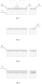
- Figures 1-10 show a method of producing an original hologram that allows the combination of dot-matrix laser and electron beam lithography techniques in a single resist layer using an aluminium interlayer.
- patterns of dot-matrix hologram (3) and alignment marks (4) in defined areas of art design are formed in a photosensitive layer (2) on a glass substrate (1) by employing laser beam interference lithography method.
- a dot-matrix hologram comprising an array of grating dots, as shown in Figure 18 , is formed by exposing designated photoresist areas to overlapping laser beams. The appropriate position and grating orientation angle of each grating dot is controlled by X-Y motorized translation stage, laser beam splitter rotation stage and computer software. Development of the exposed photoresist areas with alignment marks on the far side of specimen (5) is done using a Microposit ® MF-26A developer for 20 seconds at room temperature immersing only a far side of the specimen.
- auxiliary aluminium layer (6) with a thickness of 100 - 200 nm is evaporated on photoresist using vacuum deposition. Then a single layer of PMMA (7) is spin coated on the top of aluminium layer at 2000 - 3000 rpm for 40 seconds and dried for 5 minutes at 150oC on hotplate.
- PMMA layer thickness depends on viscosity and can vary from about 150 to 400 nm.
- Precise alignment and angle correction between the dot-matrix and electron beam patterning areas is done with a Raith e_LiNe scanning electron microscope, using dot-matrix patterned and developed alignment marks (8) that are placed on the far side of specimen (wafer coordinate system is aligned with the dot-matrix patterned area before electron beam exposure).
- Efficient electron beam patterning is done with the Gaussian beam of 2 nm size provided by Raith e_LiNe electron beam lithography system. The system requires precise focusing and alignment procedures and exposure parameters usually are customized for specific application, e.g. exposing different parts of one design and changing column and other parameters in between.
- CGH is a diffractive optical beam shaping element used to transform the transverse power distribution of a laser beam incident upon it into a desired transverse power distribution.
- CGHs as shown in Figure 20 , can be calculated by several different methods included, but not limited to, Detour Phase algorithm, Gerchberg - Saxton algorithm, Wavefront Recording Plane algorithm, Kinoform algorithm, Fourier Ping - Pong algorithm, Coherent Raytrace algorithm and Diffraction - Specific algorithm.
- Development of the exposed PMMA 9) is done in MIBK - IPA solution, ratio 1:3, for 40 seconds with agitation. Then development is stopped in IPA for 15 seconds.
- Ceric ammonium nitrate-based etchant Ce(NH 4 ) 2 (NO 3 ) 6 :HNO 3 with etch rate of 40 ⁇ /sec, at room temperature, is used for etching of the aluminium film followed by deionized water rinse. After wet chemical etching of the aluminium film (10) and soft baking on a hotplate at 90°C for 1 min, the photoresist is exposed by mercury lamp with 32 mW/cm 2 light intensity in OAI Model 200 mask aligner through the openings in the aluminium layer (11). The typical exposure time is equal to 10 seconds. Then PMMA is lifted off together with aluminium layer, as shown in Figure 9 , in ultrasound bath using ceric ammonium nitrate-based etchant.
- the final development of the photoresist in the dot-matrix laser and electron beam patterned areas is done using a Microposit ® MF-26A developer for 20 seconds at room temperature immersing whole specimen. After development procedure, whole specimen with a developed photoresist pattern (12) as shown in Figure 10 , is rinsed in distilled water and then dried using compressed nitrogen gas flow.
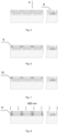
- Figures 11-17 show the formation of a multilayer polymeric film with a hologram using a single resist layer with dot-matrix and electron beam patterned and precisely aligned features.
- Vacuum evaporation technique is used to form electroconductive silver layer (13) with thickness of about 40 nm on the surface of the glass substrate (1) with a patterned PMMA layer (12).
- Boric acid is used as a buffering agent to stabilize pH value of the electrolyte in the range from 3.8 to 4.2 (optimal value is 4.0).
- Sodium dodecyl sulphate is used as an antipitting agent.
- the titanium basket filled with the Nickel S-Rounds (by INCO) and coated with a polypropylene fabric is used as an anode.
- the cathode current density is 10 mA/cm 2 during the first 15 min of electrolysis and later is smoothly increased up to 35 mA/cm 2 for the remaining time of electrolysis.
- the final thickness of the electrodeposited layer is about 90 ⁇ m and the average deposition rate is approximately 37 ⁇ m/h.
- Ni film (14) is detached from the PMMA surface and is washed with warm water.
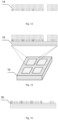
- Ni film with a mirror image of dot-matrix and electron beam patterned hologram is then used for the recombining process in order to obtain a single nickel master shim.
- the main requirement for hologram recombining equipment is to ensure precision contact across the entire embossing area. Recombining quality during embossing is dependent on the quality of the operating elements of the device and the technological parameters (temperature, pressure, processing duration and positioning accuracy). Recombining accuracy is achieved using a device with precision head and coordinate table. The material of the head is chosen in such a way that the surface properties and volume dimensions are constant during embossing process.
- Nickel coated PMMA plate is immersed into the nickel sulphamate bath in order to produce a nickel master shim (17).
- Boric acid is used as a buffering agent to stabilize pH value of the electrolyte in the range from 3.8 to 4.2 (optimal value is 4.0).
- Sodium dodecyl sulphate is used as an antipitting agent.
- the titanium basket filled with the Nickel S-Rounds (by INCO) and coated with a polypropylene fabric is used as an anode.
- the cathode current density is 10 mA/cm 2 during the first 15 min of electrolysis and later is smoothly increased up to 35 mA/cm 2 for the remaining time of electrolysis.
- the final thickness of the electrodeposited layer is about 90 ⁇ m and the average deposition rate is approximately 37 ⁇ m/h.
- a second roller presses the transparent or metalized film into the shim (18).
- Type of the multilayer film depends on the application of the final product. Simple PET or tamper evident film with thickness of 19-54 ⁇ m can be applied for the stickers production. Multilayer film with the thickness of 19-24 ⁇ m can be used for hot stamping applications. For stickers production a pressure sensitive adhesive layer with thickness of 10-25 ⁇ m is coated and sandwiched with silicone paper (19). Then different types of cutting devices, like plotters, cutting machines, etc., can be used to get required size and shape of the stickers. Very thin adhesive layer, around 1-5 ⁇ m thick, is coated for hot stamping applications.
- Coating regimes are chosen depending on nature and viscosity of adhesive.
- annilox rolls equipped with knifes can be used in order to ensure smooth and even distribution of the thin adhesive layer on the surface of polymer film.
- wire rods for adhesive layer formation can be used in case of low adhesive viscosity wire rods for adhesive layer formation. Thickness of adhesive layer depends on adhesive viscosity and wire diameter.
Landscapes
- Physics & Mathematics (AREA)
- General Physics & Mathematics (AREA)
- Engineering & Computer Science (AREA)
- Computer Security & Cryptography (AREA)
- Microelectronics & Electronic Packaging (AREA)
- Toxicology (AREA)
- Health & Medical Sciences (AREA)
- Optics & Photonics (AREA)
- Business, Economics & Management (AREA)
- Accounting & Taxation (AREA)
- Finance (AREA)
- Holo Graphy (AREA)
- Credit Cards Or The Like (AREA)
Claims (2)
- Procédé permettant de fabriquer une étiquette de sécurité holographique, comprenant les étapes consistant à :structurer par laser à matrice de points un hologramme (3) dans des zones de motif définies et des repères d'alignement (4) dans une couche de photorésine (2) sur un substrat de verre ;développer des zones de photorésine exposées avec les repères d'alignement (4) sur une face éloignée (5) de la couche de photorésine sur le substrat de verre formant un spécimen ;déposer sous vide un film d'aluminium auxiliaire (6) d'une épaisseur de 100 à 200 nm ;enduire par centrifugation une seule couche de PMMA (7) ;effectuer un alignement précis et une correction d'angle entre les zones de structuration à matrice de points et par faisceau d'électrons (8) par microscope électronique à balayage ;structurer par faisceau d'électrons ;développer le PMMA (9) ;graver le film d'aluminium (10) au Ce(NH4)2(NO3)6:HNO3 ;exposer la photorésine (λ = 405 nm) ;enlever le PMMA (9) et la couche d'aluminium gravée (10) ;développer définitivement la photorésine en fabriquant des zones alignées d'un hologramme (12) structuré par matrice de points et par faisceau d'électrons (12) ;déposer sous vide un film d'argent (13) ;déposer de manière électrochimique un film de nickel (14) ;produire une cale de nickel (17) pour une reproduction de rouleau à rouleau ;reproduire les hologrammes dans un film polymère métallisé ou transparent multicouche (18) ;enduire le film (18) d'un adhésif (19) sensible à la pression, thermoplastique ou thermodurcissable, et diviser en étiquettes individuelles.
- Etiquette de sécurité holographique obtenue par le procédé de la revendication 1.
Priority Applications (3)
| Application Number | Priority Date | Filing Date | Title |
|---|---|---|---|
| EP20169233.2A EP3896529B1 (fr) | 2020-04-13 | 2020-04-13 | Procédé de fabrication d'étiquette de sécurité holographique |
| JP2021006841A JP7000647B2 (ja) | 2020-04-13 | 2021-01-20 | ホログラフィックセキュリティラベルの製造方法 |
| US17/178,281 US11846888B2 (en) | 2020-04-13 | 2021-02-18 | Fabrication method of holographic security label |
Applications Claiming Priority (1)
| Application Number | Priority Date | Filing Date | Title |
|---|---|---|---|
| EP20169233.2A EP3896529B1 (fr) | 2020-04-13 | 2020-04-13 | Procédé de fabrication d'étiquette de sécurité holographique |
Publications (3)
| Publication Number | Publication Date |
|---|---|
| EP3896529A1 EP3896529A1 (fr) | 2021-10-20 |
| EP3896529C0 EP3896529C0 (fr) | 2024-08-28 |
| EP3896529B1 true EP3896529B1 (fr) | 2024-08-28 |
Family
ID=70289282
Family Applications (1)
| Application Number | Title | Priority Date | Filing Date |
|---|---|---|---|
| EP20169233.2A Active EP3896529B1 (fr) | 2020-04-13 | 2020-04-13 | Procédé de fabrication d'étiquette de sécurité holographique |
Country Status (3)
| Country | Link |
|---|---|
| US (1) | US11846888B2 (fr) |
| EP (1) | EP3896529B1 (fr) |
| JP (1) | JP7000647B2 (fr) |
Families Citing this family (2)
| Publication number | Priority date | Publication date | Assignee | Title |
|---|---|---|---|---|
| CN116198064B (zh) * | 2023-03-01 | 2024-11-19 | 青岛中兴通轨道交通科技有限公司 | 一种夹胶聚碳酸酯板的高压成型方法 |
| CN120339455B (zh) * | 2024-04-15 | 2026-03-31 | 武汉铭宇光电技术有限公司 | 动态全息防伪图案生成方法、系统、计算机及存储介质 |
Citations (1)
| Publication number | Priority date | Publication date | Assignee | Title |
|---|---|---|---|---|
| EP2152526B1 (fr) * | 2007-06-13 | 2011-09-07 | De La Rue International Limited | Dispositif de sécurité holographique |
Family Cites Families (14)
| Publication number | Priority date | Publication date | Assignee | Title |
|---|---|---|---|---|
| JPS5418160U (fr) * | 1977-04-14 | 1979-02-06 | ||
| US5413884A (en) | 1992-12-14 | 1995-05-09 | American Telephone And Telegraph Company | Grating fabrication using electron beam lithography |
| US5393634A (en) | 1993-05-27 | 1995-02-28 | The United States Of America As Represented By The Administrator Of The National Aeronautics And Space Administration | Continuous phase and amplitude holographic elements |
| US6392768B1 (en) | 1999-09-16 | 2002-05-21 | Ahead Optoelectronics, Inc. | Dot matrix hologram with a hidden image |
| GB0117391D0 (en) | 2001-07-17 | 2001-09-05 | Optaglio Ltd | Optical device and method of manufacture |
| US6756296B2 (en) * | 2001-12-11 | 2004-06-29 | California Institute Of Technology | Method for lithographic processing on molecular monolayer and multilayer thin films |
| GB0601093D0 (en) | 2006-01-19 | 2006-03-01 | Rue De Int Ltd | Optically Variable Security Device |
| DE102007043149B4 (de) | 2007-09-03 | 2016-09-29 | Seereal Technologies S.A. | Verfahren und Vorrichtung zum Übertragen von holografischen Videodaten |
| JP2012150272A (ja) | 2011-01-19 | 2012-08-09 | Dainippon Printing Co Ltd | ホログラムラベル |
| KR101820563B1 (ko) | 2014-12-31 | 2018-01-19 | 한국전자통신연구원 | 홀로그램 데이터 포맷과 홀로그래픽 비디오 시스템 장치 및 방법 |
| CN105807348B (zh) | 2016-05-23 | 2018-07-06 | 东南大学 | 一种反射型体全息光栅波导结构 |
| KR102732515B1 (ko) | 2016-11-10 | 2024-11-20 | 삼성전자주식회사 | 확장된 시야창을 제공하는 홀로그래픽 디스플레이 장치 |
| CN107167920B (zh) | 2017-06-19 | 2020-06-30 | 东南大学 | 一种高亮度全息波导显示装置 |
| GB2572746B (en) * | 2018-03-22 | 2021-10-27 | De La Rue Int Ltd | Security elements and method of manufacture thereof |
-
2020
- 2020-04-13 EP EP20169233.2A patent/EP3896529B1/fr active Active
-
2021
- 2021-01-20 JP JP2021006841A patent/JP7000647B2/ja active Active
- 2021-02-18 US US17/178,281 patent/US11846888B2/en active Active
Patent Citations (1)
| Publication number | Priority date | Publication date | Assignee | Title |
|---|---|---|---|---|
| EP2152526B1 (fr) * | 2007-06-13 | 2011-09-07 | De La Rue International Limited | Dispositif de sécurité holographique |
Also Published As
| Publication number | Publication date |
|---|---|
| JP7000647B2 (ja) | 2022-01-19 |
| EP3896529A1 (fr) | 2021-10-20 |
| US20210318621A1 (en) | 2021-10-14 |
| EP3896529C0 (fr) | 2024-08-28 |
| US11846888B2 (en) | 2023-12-19 |
| JP2021170104A (ja) | 2021-10-28 |
Similar Documents
| Publication | Publication Date | Title |
|---|---|---|
| EP2152526B1 (fr) | Dispositif de sécurité holographique | |
| CN101115627B (zh) | 包括衍射浮雕结构的多层体及其制备方法、用途 | |
| US20010041307A1 (en) | Three-dimensional microstructure | |
| US11846888B2 (en) | Fabrication method of holographic security label | |
| US7241537B2 (en) | Method for producing an exposed substrate | |
| EP1974241B1 (fr) | Procédé pour la fabrication d'un article de sécurité optiquement variable | |
| CN109291673A (zh) | 一种精确镀铝的图案化全息防伪器件及其制备方法 | |
| EP1706280B1 (fr) | Document avec dispositif de sécurité, plaque ou cylindre d'impression pour l'application du dispositif de sécurité et procédé de production de la plaque ou du cylindre d'impression | |
| RU2035763C1 (ru) | Способ изготовления голографических меток | |
| RU2035314C1 (ru) | Способ изготовления голографических этикеток | |
| KR102214046B1 (ko) | 보안용 홀로그램 스티커 라벨의 제조방법 | |
| JP2005242357A (ja) | 表面上に回折要素を被着させるための方法及び装置 | |
| KR20110093779A (ko) | 개선된 다축 회절 격자 | |
| KR100913200B1 (ko) | 표시판 및 그 제조 방법 | |
| AU749702B2 (en) | Three-dimensional microstructure | |
| AU2011100389B4 (en) | Micro/nano structure origination method | |
| CN115100944A (zh) | 基于衍射光学与激光全息的双重防伪结构及制备方法 | |
| Luciani et al. | Multiple-level technique for high-resolution OVDs fabrication | |
| LT6393B (lt) | Kombinuotas holograminis lipdukas |
Legal Events
| Date | Code | Title | Description |
|---|---|---|---|
| PUAI | Public reference made under article 153(3) epc to a published international application that has entered the european phase |
Free format text: ORIGINAL CODE: 0009012 |
|
| STAA | Information on the status of an ep patent application or granted ep patent |
Free format text: STATUS: THE APPLICATION HAS BEEN PUBLISHED |
|
| AK | Designated contracting states |
Kind code of ref document: A1 Designated state(s): AL AT BE BG CH CY CZ DE DK EE ES FI FR GB GR HR HU IE IS IT LI LT LU LV MC MK MT NL NO PL PT RO RS SE SI SK SM TR |
|
| B565 | Issuance of search results under rule 164(2) epc |
Effective date: 20200921 |
|
| STAA | Information on the status of an ep patent application or granted ep patent |
Free format text: STATUS: REQUEST FOR EXAMINATION WAS MADE |
|
| 17P | Request for examination filed |
Effective date: 20200414 |
|
| RIC1 | Information provided on ipc code assigned before grant |
Ipc: G03H 1/30 20060101ALN20231201BHEP Ipc: G03H 1/02 20060101ALN20231201BHEP Ipc: G03H 1/00 20060101AFI20231201BHEP |
|
| RIC1 | Information provided on ipc code assigned before grant |
Ipc: G03H 1/30 20060101ALN20240125BHEP Ipc: G03H 1/02 20060101ALN20240125BHEP Ipc: G03H 1/00 20060101AFI20240125BHEP |
|
| RIC1 | Information provided on ipc code assigned before grant |
Ipc: G03H 1/30 20060101ALN20240214BHEP Ipc: G03H 1/02 20060101ALN20240214BHEP Ipc: G03H 1/00 20060101AFI20240214BHEP |
|
| GRAP | Despatch of communication of intention to grant a patent |
Free format text: ORIGINAL CODE: EPIDOSNIGR1 |
|
| STAA | Information on the status of an ep patent application or granted ep patent |
Free format text: STATUS: GRANT OF PATENT IS INTENDED |
|
| GRAS | Grant fee paid |
Free format text: ORIGINAL CODE: EPIDOSNIGR3 |
|
| RIC1 | Information provided on ipc code assigned before grant |
Ipc: G03H 1/30 20060101ALN20240307BHEP Ipc: G03H 1/02 20060101ALN20240307BHEP Ipc: G03H 1/00 20060101AFI20240307BHEP |
|
| INTG | Intention to grant announced |
Effective date: 20240326 |
|
| GRAA | (expected) grant |
Free format text: ORIGINAL CODE: 0009210 |
|
| STAA | Information on the status of an ep patent application or granted ep patent |
Free format text: STATUS: THE PATENT HAS BEEN GRANTED |
|
| AK | Designated contracting states |
Kind code of ref document: B1 Designated state(s): AL AT BE BG CH CY CZ DE DK EE ES FI FR GB GR HR HU IE IS IT LI LT LU LV MC MK MT NL NO PL PT RO RS SE SI SK SM TR |
|
| REG | Reference to a national code |
Ref country code: CH Ref legal event code: EP |
|
| REG | Reference to a national code |
Ref country code: DE Ref legal event code: R096 Ref document number: 602020036509 Country of ref document: DE |
|
| REG | Reference to a national code |
Ref country code: IE Ref legal event code: FG4D |
|
| U01 | Request for unitary effect filed |
Effective date: 20240906 |
|
| U07 | Unitary effect registered |
Designated state(s): AT BE BG DE DK EE FI FR IT LT LU LV MT NL PT RO SE SI Effective date: 20240923 |
|
| PG25 | Lapsed in a contracting state [announced via postgrant information from national office to epo] |
Ref country code: NO Free format text: LAPSE BECAUSE OF FAILURE TO SUBMIT A TRANSLATION OF THE DESCRIPTION OR TO PAY THE FEE WITHIN THE PRESCRIBED TIME-LIMIT Effective date: 20241128 |
|
| PG25 | Lapsed in a contracting state [announced via postgrant information from national office to epo] |
Ref country code: GR Free format text: LAPSE BECAUSE OF FAILURE TO SUBMIT A TRANSLATION OF THE DESCRIPTION OR TO PAY THE FEE WITHIN THE PRESCRIBED TIME-LIMIT Effective date: 20241129 Ref country code: PL Free format text: LAPSE BECAUSE OF FAILURE TO SUBMIT A TRANSLATION OF THE DESCRIPTION OR TO PAY THE FEE WITHIN THE PRESCRIBED TIME-LIMIT Effective date: 20240828 |
|
| PG25 | Lapsed in a contracting state [announced via postgrant information from national office to epo] |
Ref country code: IS Free format text: LAPSE BECAUSE OF FAILURE TO SUBMIT A TRANSLATION OF THE DESCRIPTION OR TO PAY THE FEE WITHIN THE PRESCRIBED TIME-LIMIT Effective date: 20241228 |
|
| PG25 | Lapsed in a contracting state [announced via postgrant information from national office to epo] |
Ref country code: HR Free format text: LAPSE BECAUSE OF FAILURE TO SUBMIT A TRANSLATION OF THE DESCRIPTION OR TO PAY THE FEE WITHIN THE PRESCRIBED TIME-LIMIT Effective date: 20240828 |
|
| PG25 | Lapsed in a contracting state [announced via postgrant information from national office to epo] |
Ref country code: RS Free format text: LAPSE BECAUSE OF FAILURE TO SUBMIT A TRANSLATION OF THE DESCRIPTION OR TO PAY THE FEE WITHIN THE PRESCRIBED TIME-LIMIT Effective date: 20241128 Ref country code: ES Free format text: LAPSE BECAUSE OF FAILURE TO SUBMIT A TRANSLATION OF THE DESCRIPTION OR TO PAY THE FEE WITHIN THE PRESCRIBED TIME-LIMIT Effective date: 20240828 |
|
| PG25 | Lapsed in a contracting state [announced via postgrant information from national office to epo] |
Ref country code: RS Free format text: LAPSE BECAUSE OF FAILURE TO SUBMIT A TRANSLATION OF THE DESCRIPTION OR TO PAY THE FEE WITHIN THE PRESCRIBED TIME-LIMIT Effective date: 20241128 Ref country code: PL Free format text: LAPSE BECAUSE OF FAILURE TO SUBMIT A TRANSLATION OF THE DESCRIPTION OR TO PAY THE FEE WITHIN THE PRESCRIBED TIME-LIMIT Effective date: 20240828 Ref country code: NO Free format text: LAPSE BECAUSE OF FAILURE TO SUBMIT A TRANSLATION OF THE DESCRIPTION OR TO PAY THE FEE WITHIN THE PRESCRIBED TIME-LIMIT Effective date: 20241128 Ref country code: IS Free format text: LAPSE BECAUSE OF FAILURE TO SUBMIT A TRANSLATION OF THE DESCRIPTION OR TO PAY THE FEE WITHIN THE PRESCRIBED TIME-LIMIT Effective date: 20241228 Ref country code: HR Free format text: LAPSE BECAUSE OF FAILURE TO SUBMIT A TRANSLATION OF THE DESCRIPTION OR TO PAY THE FEE WITHIN THE PRESCRIBED TIME-LIMIT Effective date: 20240828 Ref country code: GR Free format text: LAPSE BECAUSE OF FAILURE TO SUBMIT A TRANSLATION OF THE DESCRIPTION OR TO PAY THE FEE WITHIN THE PRESCRIBED TIME-LIMIT Effective date: 20241129 Ref country code: ES Free format text: LAPSE BECAUSE OF FAILURE TO SUBMIT A TRANSLATION OF THE DESCRIPTION OR TO PAY THE FEE WITHIN THE PRESCRIBED TIME-LIMIT Effective date: 20240828 |
|
| PG25 | Lapsed in a contracting state [announced via postgrant information from national office to epo] |
Ref country code: SM Free format text: LAPSE BECAUSE OF FAILURE TO SUBMIT A TRANSLATION OF THE DESCRIPTION OR TO PAY THE FEE WITHIN THE PRESCRIBED TIME-LIMIT Effective date: 20240828 |
|
| PG25 | Lapsed in a contracting state [announced via postgrant information from national office to epo] |
Ref country code: CZ Free format text: LAPSE BECAUSE OF FAILURE TO SUBMIT A TRANSLATION OF THE DESCRIPTION OR TO PAY THE FEE WITHIN THE PRESCRIBED TIME-LIMIT Effective date: 20240828 |
|
| PG25 | Lapsed in a contracting state [announced via postgrant information from national office to epo] |
Ref country code: SK Free format text: LAPSE BECAUSE OF FAILURE TO SUBMIT A TRANSLATION OF THE DESCRIPTION OR TO PAY THE FEE WITHIN THE PRESCRIBED TIME-LIMIT Effective date: 20240828 |
|
| U20 | Renewal fee for the european patent with unitary effect paid |
Year of fee payment: 6 Effective date: 20250422 |
|
| PLBE | No opposition filed within time limit |
Free format text: ORIGINAL CODE: 0009261 |
|
| STAA | Information on the status of an ep patent application or granted ep patent |
Free format text: STATUS: NO OPPOSITION FILED WITHIN TIME LIMIT |
|
| 26N | No opposition filed |
Effective date: 20250530 |
|
| REG | Reference to a national code |
Ref country code: CH Ref legal event code: H13 Free format text: ST27 STATUS EVENT CODE: U-0-0-H10-H13 (AS PROVIDED BY THE NATIONAL OFFICE) Effective date: 20251125 |
|
| PG25 | Lapsed in a contracting state [announced via postgrant information from national office to epo] |
Ref country code: MC Free format text: LAPSE BECAUSE OF FAILURE TO SUBMIT A TRANSLATION OF THE DESCRIPTION OR TO PAY THE FEE WITHIN THE PRESCRIBED TIME-LIMIT Effective date: 20240828 |
|
| GBPC | Gb: european patent ceased through non-payment of renewal fee |
Effective date: 20250413 |
|
| PG25 | Lapsed in a contracting state [announced via postgrant information from national office to epo] |
Ref country code: GB Free format text: LAPSE BECAUSE OF NON-PAYMENT OF DUE FEES Effective date: 20250413 |
|
| PG25 | Lapsed in a contracting state [announced via postgrant information from national office to epo] |
Ref country code: CH Free format text: LAPSE BECAUSE OF NON-PAYMENT OF DUE FEES Effective date: 20250430 |
|
| PG25 | Lapsed in a contracting state [announced via postgrant information from national office to epo] |
Ref country code: IE Free format text: LAPSE BECAUSE OF NON-PAYMENT OF DUE FEES Effective date: 20250413 |