EP3899645B1 - Procédé de formation de réseaux - Google Patents
Procédé de formation de réseaux Download PDFInfo
- Publication number
- EP3899645B1 EP3899645B1 EP19900530.7A EP19900530A EP3899645B1 EP 3899645 B1 EP3899645 B1 EP 3899645B1 EP 19900530 A EP19900530 A EP 19900530A EP 3899645 B1 EP3899645 B1 EP 3899645B1
- Authority
- EP
- European Patent Office
- Prior art keywords
- ion beam
- profile
- gratings
- substrate
- angle
- Prior art date
- Legal status (The legal status is an assumption and is not a legal conclusion. Google has not performed a legal analysis and makes no representation as to the accuracy of the status listed.)
- Active
Links
Images





Classifications
-
- G—PHYSICS
- G02—OPTICS
- G02B—OPTICAL ELEMENTS, SYSTEMS OR APPARATUS
- G02B27/00—Optical systems or apparatus not provided for by any of the groups G02B1/00 - G02B26/00, G02B30/00
- G02B27/42—Diffraction optics, i.e. systems including a diffractive element being designed for providing a diffractive effect
-
- G—PHYSICS
- G03—PHOTOGRAPHY; CINEMATOGRAPHY; ANALOGOUS TECHNIQUES USING WAVES OTHER THAN OPTICAL WAVES; ELECTROGRAPHY; HOLOGRAPHY
- G03F—PHOTOMECHANICAL PRODUCTION OF TEXTURED OR PATTERNED SURFACES, e.g. FOR PRINTING, FOR PROCESSING OF SEMICONDUCTOR DEVICES; MATERIALS THEREFOR; ORIGINALS THEREFOR; APPARATUS SPECIALLY ADAPTED THEREFOR
- G03F7/00—Photomechanical, e.g. photolithographic, production of textured or patterned surfaces, e.g. printing surfaces; Materials therefor, e.g. comprising photoresists; Apparatus specially adapted therefor
- G03F7/20—Exposure; Apparatus therefor
- G03F7/2051—Exposure without an original mask, e.g. using a programmed deflection of a point source, by scanning, by drawing with a light beam, using an addressed light or corpuscular source
- G03F7/2059—Exposure without an original mask, e.g. using a programmed deflection of a point source, by scanning, by drawing with a light beam, using an addressed light or corpuscular source using a scanning corpuscular radiation beam, e.g. an electron beam
- G03F7/2065—Exposure without an original mask, e.g. using a programmed deflection of a point source, by scanning, by drawing with a light beam, using an addressed light or corpuscular source using a scanning corpuscular radiation beam, e.g. an electron beam using corpuscular radiation other than electron beams
-
- B—PERFORMING OPERATIONS; TRANSPORTING
- B29—WORKING OF PLASTICS; WORKING OF SUBSTANCES IN A PLASTIC STATE IN GENERAL
- B29D—PRODUCING PARTICULAR ARTICLES FROM PLASTICS OR FROM SUBSTANCES IN A PLASTIC STATE
- B29D11/00—Producing optical elements, e.g. lenses or prisms
- B29D11/0074—Production of other optical elements not provided for in B29D11/00009- B29D11/0073
- B29D11/00769—Producing diffraction gratings
-
- C—CHEMISTRY; METALLURGY
- C23—COATING METALLIC MATERIAL; COATING MATERIAL WITH METALLIC MATERIAL; CHEMICAL SURFACE TREATMENT; DIFFUSION TREATMENT OF METALLIC MATERIAL; COATING BY VACUUM EVAPORATION, BY SPUTTERING, BY ION IMPLANTATION OR BY CHEMICAL VAPOUR DEPOSITION, IN GENERAL; INHIBITING CORROSION OF METALLIC MATERIAL OR INCRUSTATION IN GENERAL
- C23C—COATING METALLIC MATERIAL; COATING MATERIAL WITH METALLIC MATERIAL; SURFACE TREATMENT OF METALLIC MATERIAL BY DIFFUSION INTO THE SURFACE, BY CHEMICAL CONVERSION OR SUBSTITUTION; COATING BY VACUUM EVAPORATION, BY SPUTTERING, BY ION IMPLANTATION OR BY CHEMICAL VAPOUR DEPOSITION, IN GENERAL
- C23C14/00—Coating by vacuum evaporation, by sputtering or by ion implantation of the coating forming material
- C23C14/22—Coating by vacuum evaporation, by sputtering or by ion implantation of the coating forming material characterised by the process of coating
- C23C14/221—Ion beam deposition
-
- C—CHEMISTRY; METALLURGY
- C23—COATING METALLIC MATERIAL; COATING MATERIAL WITH METALLIC MATERIAL; CHEMICAL SURFACE TREATMENT; DIFFUSION TREATMENT OF METALLIC MATERIAL; COATING BY VACUUM EVAPORATION, BY SPUTTERING, BY ION IMPLANTATION OR BY CHEMICAL VAPOUR DEPOSITION, IN GENERAL; INHIBITING CORROSION OF METALLIC MATERIAL OR INCRUSTATION IN GENERAL
- C23C—COATING METALLIC MATERIAL; COATING MATERIAL WITH METALLIC MATERIAL; SURFACE TREATMENT OF METALLIC MATERIAL BY DIFFUSION INTO THE SURFACE, BY CHEMICAL CONVERSION OR SUBSTITUTION; COATING BY VACUUM EVAPORATION, BY SPUTTERING, BY ION IMPLANTATION OR BY CHEMICAL VAPOUR DEPOSITION, IN GENERAL
- C23C14/00—Coating by vacuum evaporation, by sputtering or by ion implantation of the coating forming material
- C23C14/22—Coating by vacuum evaporation, by sputtering or by ion implantation of the coating forming material characterised by the process of coating
- C23C14/54—Controlling or regulating the coating process
-
- C—CHEMISTRY; METALLURGY
- C23—COATING METALLIC MATERIAL; COATING MATERIAL WITH METALLIC MATERIAL; CHEMICAL SURFACE TREATMENT; DIFFUSION TREATMENT OF METALLIC MATERIAL; COATING BY VACUUM EVAPORATION, BY SPUTTERING, BY ION IMPLANTATION OR BY CHEMICAL VAPOUR DEPOSITION, IN GENERAL; INHIBITING CORROSION OF METALLIC MATERIAL OR INCRUSTATION IN GENERAL
- C23C—COATING METALLIC MATERIAL; COATING MATERIAL WITH METALLIC MATERIAL; SURFACE TREATMENT OF METALLIC MATERIAL BY DIFFUSION INTO THE SURFACE, BY CHEMICAL CONVERSION OR SUBSTITUTION; COATING BY VACUUM EVAPORATION, BY SPUTTERING, BY ION IMPLANTATION OR BY CHEMICAL VAPOUR DEPOSITION, IN GENERAL
- C23C14/00—Coating by vacuum evaporation, by sputtering or by ion implantation of the coating forming material
- C23C14/22—Coating by vacuum evaporation, by sputtering or by ion implantation of the coating forming material characterised by the process of coating
- C23C14/56—Apparatus specially adapted for continuous coating; Arrangements for maintaining the vacuum, e.g. vacuum locks
- C23C14/562—Apparatus specially adapted for continuous coating; Arrangements for maintaining the vacuum, e.g. vacuum locks for coating elongated substrates
-
- C—CHEMISTRY; METALLURGY
- C23—COATING METALLIC MATERIAL; COATING MATERIAL WITH METALLIC MATERIAL; CHEMICAL SURFACE TREATMENT; DIFFUSION TREATMENT OF METALLIC MATERIAL; COATING BY VACUUM EVAPORATION, BY SPUTTERING, BY ION IMPLANTATION OR BY CHEMICAL VAPOUR DEPOSITION, IN GENERAL; INHIBITING CORROSION OF METALLIC MATERIAL OR INCRUSTATION IN GENERAL
- C23C—COATING METALLIC MATERIAL; COATING MATERIAL WITH METALLIC MATERIAL; SURFACE TREATMENT OF METALLIC MATERIAL BY DIFFUSION INTO THE SURFACE, BY CHEMICAL CONVERSION OR SUBSTITUTION; COATING BY VACUUM EVAPORATION, BY SPUTTERING, BY ION IMPLANTATION OR BY CHEMICAL VAPOUR DEPOSITION, IN GENERAL
- C23C14/00—Coating by vacuum evaporation, by sputtering or by ion implantation of the coating forming material
- C23C14/22—Coating by vacuum evaporation, by sputtering or by ion implantation of the coating forming material characterised by the process of coating
- C23C14/56—Apparatus specially adapted for continuous coating; Arrangements for maintaining the vacuum, e.g. vacuum locks
- C23C14/568—Transferring the substrates through a series of coating stations
-
- G—PHYSICS
- G02—OPTICS
- G02B—OPTICAL ELEMENTS, SYSTEMS OR APPARATUS
- G02B27/00—Optical systems or apparatus not provided for by any of the groups G02B1/00 - G02B26/00, G02B30/00
- G02B27/01—Head-up displays
- G02B27/017—Head mounted
- G02B27/0172—Head mounted characterised by optical features
-
- G—PHYSICS
- G02—OPTICS
- G02B—OPTICAL ELEMENTS, SYSTEMS OR APPARATUS
- G02B3/00—Simple or compound lenses
- G02B3/0006—Arrays
- G02B3/0012—Arrays characterised by the manufacturing method
- G02B3/0018—Reflow, i.e. characterized by the step of melting microstructures to form curved surfaces, e.g. manufacturing of moulds and surfaces for transfer etching
-
- G—PHYSICS
- G02—OPTICS
- G02B—OPTICAL ELEMENTS, SYSTEMS OR APPARATUS
- G02B30/00—Optical systems or apparatus for producing three-dimensional [3D] effects, e.g. stereoscopic images
-
- G—PHYSICS
- G02—OPTICS
- G02B—OPTICAL ELEMENTS, SYSTEMS OR APPARATUS
- G02B5/00—Optical elements other than lenses
- G02B5/18—Diffraction gratings
- G02B5/1847—Manufacturing methods
- G02B5/1857—Manufacturing methods using exposure or etching means, e.g. holography, photolithography, exposure to electron or ion beams
-
- G—PHYSICS
- G03—PHOTOGRAPHY; CINEMATOGRAPHY; ANALOGOUS TECHNIQUES USING WAVES OTHER THAN OPTICAL WAVES; ELECTROGRAPHY; HOLOGRAPHY
- G03F—PHOTOMECHANICAL PRODUCTION OF TEXTURED OR PATTERNED SURFACES, e.g. FOR PRINTING, FOR PROCESSING OF SEMICONDUCTOR DEVICES; MATERIALS THEREFOR; ORIGINALS THEREFOR; APPARATUS SPECIALLY ADAPTED THEREFOR
- G03F7/00—Photomechanical, e.g. photolithographic, production of textured or patterned surfaces, e.g. printing surfaces; Materials therefor, e.g. comprising photoresists; Apparatus specially adapted therefor
- G03F7/0005—Production of optical devices or components in so far as characterised by the lithographic processes or materials used therefor
- G03F7/001—Phase modulating patterns, e.g. refractive index patterns
-
- G—PHYSICS
- G03—PHOTOGRAPHY; CINEMATOGRAPHY; ANALOGOUS TECHNIQUES USING WAVES OTHER THAN OPTICAL WAVES; ELECTROGRAPHY; HOLOGRAPHY
- G03F—PHOTOMECHANICAL PRODUCTION OF TEXTURED OR PATTERNED SURFACES, e.g. FOR PRINTING, FOR PROCESSING OF SEMICONDUCTOR DEVICES; MATERIALS THEREFOR; ORIGINALS THEREFOR; APPARATUS SPECIALLY ADAPTED THEREFOR
- G03F7/00—Photomechanical, e.g. photolithographic, production of textured or patterned surfaces, e.g. printing surfaces; Materials therefor, e.g. comprising photoresists; Apparatus specially adapted therefor
- G03F7/16—Coating processes; Apparatus therefor
-
- G—PHYSICS
- G03—PHOTOGRAPHY; CINEMATOGRAPHY; ANALOGOUS TECHNIQUES USING WAVES OTHER THAN OPTICAL WAVES; ELECTROGRAPHY; HOLOGRAPHY
- G03F—PHOTOMECHANICAL PRODUCTION OF TEXTURED OR PATTERNED SURFACES, e.g. FOR PRINTING, FOR PROCESSING OF SEMICONDUCTOR DEVICES; MATERIALS THEREFOR; ORIGINALS THEREFOR; APPARATUS SPECIALLY ADAPTED THEREFOR
- G03F7/00—Photomechanical, e.g. photolithographic, production of textured or patterned surfaces, e.g. printing surfaces; Materials therefor, e.g. comprising photoresists; Apparatus specially adapted therefor
- G03F7/20—Exposure; Apparatus therefor
- G03F7/2002—Exposure; Apparatus therefor with visible light or UV light, through an original having an opaque pattern on a transparent support, e.g. film printing, projection printing; by reflection of visible or UV light from an original such as a printed image
-
- G—PHYSICS
- G03—PHOTOGRAPHY; CINEMATOGRAPHY; ANALOGOUS TECHNIQUES USING WAVES OTHER THAN OPTICAL WAVES; ELECTROGRAPHY; HOLOGRAPHY
- G03F—PHOTOMECHANICAL PRODUCTION OF TEXTURED OR PATTERNED SURFACES, e.g. FOR PRINTING, FOR PROCESSING OF SEMICONDUCTOR DEVICES; MATERIALS THEREFOR; ORIGINALS THEREFOR; APPARATUS SPECIALLY ADAPTED THEREFOR
- G03F7/00—Photomechanical, e.g. photolithographic, production of textured or patterned surfaces, e.g. printing surfaces; Materials therefor, e.g. comprising photoresists; Apparatus specially adapted therefor
- G03F7/20—Exposure; Apparatus therefor
- G03F7/2022—Multi-step exposure, e.g. hybrid; backside exposure; blanket exposure, e.g. for image reversal; edge exposure, e.g. for edge bead removal; corrective exposure
- G03F7/2032—Simultaneous exposure of the front side and the backside
-
- G—PHYSICS
- G03—PHOTOGRAPHY; CINEMATOGRAPHY; ANALOGOUS TECHNIQUES USING WAVES OTHER THAN OPTICAL WAVES; ELECTROGRAPHY; HOLOGRAPHY
- G03F—PHOTOMECHANICAL PRODUCTION OF TEXTURED OR PATTERNED SURFACES, e.g. FOR PRINTING, FOR PROCESSING OF SEMICONDUCTOR DEVICES; MATERIALS THEREFOR; ORIGINALS THEREFOR; APPARATUS SPECIALLY ADAPTED THEREFOR
- G03F7/00—Photomechanical, e.g. photolithographic, production of textured or patterned surfaces, e.g. printing surfaces; Materials therefor, e.g. comprising photoresists; Apparatus specially adapted therefor
- G03F7/20—Exposure; Apparatus therefor
- G03F7/24—Curved surfaces
-
- H—ELECTRICITY
- H01—ELECTRIC ELEMENTS
- H01J—ELECTRIC DISCHARGE TUBES OR DISCHARGE LAMPS
- H01J37/00—Discharge tubes with provision for introducing objects or material to be exposed to the discharge, e.g. for the purpose of examination or processing thereof
- H01J37/30—Electron-beam or ion-beam tubes for localised treatment of objects
- H01J37/305—Electron-beam or ion-beam tubes for localised treatment of objects for casting, melting, evaporating, or etching
-
- H—ELECTRICITY
- H01—ELECTRIC ELEMENTS
- H01J—ELECTRIC DISCHARGE TUBES OR DISCHARGE LAMPS
- H01J37/00—Discharge tubes with provision for introducing objects or material to be exposed to the discharge, e.g. for the purpose of examination or processing thereof
- H01J37/30—Electron-beam or ion-beam tubes for localised treatment of objects
- H01J37/31—Electron-beam or ion-beam tubes for localised treatment of objects for cutting or drilling
-
- H—ELECTRICITY
- H01—ELECTRIC ELEMENTS
- H01J—ELECTRIC DISCHARGE TUBES OR DISCHARGE LAMPS
- H01J37/00—Discharge tubes with provision for introducing objects or material to be exposed to the discharge, e.g. for the purpose of examination or processing thereof
- H01J37/30—Electron-beam or ion-beam tubes for localised treatment of objects
- H01J37/317—Electron-beam or ion-beam tubes for localised treatment of objects for changing properties of the objects or for applying thin layers thereon, e.g. for ion implantation
-
- G—PHYSICS
- G02—OPTICS
- G02B—OPTICAL ELEMENTS, SYSTEMS OR APPARATUS
- G02B6/00—Light guides; Structural details of arrangements comprising light guides and other optical elements, e.g. couplings
- G02B6/0001—Light guides; Structural details of arrangements comprising light guides and other optical elements, e.g. couplings specially adapted for lighting devices or systems
- G02B6/0011—Light guides; Structural details of arrangements comprising light guides and other optical elements, e.g. couplings specially adapted for lighting devices or systems the light guides being planar or of plate-like form
- G02B6/0013—Means for improving the coupling-in of light from the light source into the light guide
- G02B6/0015—Means for improving the coupling-in of light from the light source into the light guide provided on the surface of the light guide or in the bulk of it
- G02B6/0016—Grooves, prisms, gratings, scattering particles or rough surfaces
-
- G—PHYSICS
- G02—OPTICS
- G02B—OPTICAL ELEMENTS, SYSTEMS OR APPARATUS
- G02B6/00—Light guides; Structural details of arrangements comprising light guides and other optical elements, e.g. couplings
- G02B6/0001—Light guides; Structural details of arrangements comprising light guides and other optical elements, e.g. couplings specially adapted for lighting devices or systems
- G02B6/0011—Light guides; Structural details of arrangements comprising light guides and other optical elements, e.g. couplings specially adapted for lighting devices or systems the light guides being planar or of plate-like form
- G02B6/0065—Manufacturing aspects; Material aspects
Definitions
- Embodiments of the present disclosure generally relate to a method and, more specifically, to a method of forming gratings.
- Virtual reality is generally considered to be a computer generated simulated environment in which a user has an apparent physical presence.
- a virtual reality experience can be generated in 3D and viewed with a head-mounted display (HMD), such as glasses or other wearable display devices that have near-eye display panels as lenses to display a virtual reality environment that replaces an actual environment.
- HMD head-mounted display
- Augmented reality enables an experience in which a user can still see through the display lenses of the glasses or other HMD device to view the surrounding environment, yet also see images of virtual objects that are generated for display and appear as part of the environment.
- Augmented reality can include any type of input, such as audio and haptic inputs, as well as virtual images, graphics, and video that enhances or augments the environment that the user experiences.
- a virtual image is overlaid on an ambient environment to provide an augmented reality experience to the user.
- Waveguides are used to assist in overlaying images. Generated light is propagated through a waveguide until the light exits the waveguide and is overlaid on the ambient environment.
- Optical devices generally need multiple waveguides with different physical properties on the same substrate in order to guide light of different wavelengths.
- Embodiments of the disclosure generally relate to methods of forming gratings.
- a resist layer is disposed over grating material and patterned, allowing for more accurate formation of gratings with desired grating profiles.
- a method according to the invention is specified in the appended claim 1. Additional aspects of the invention are furthermore specified in the appended claims and included in the following embodiments.
- a method of forming gratings includes depositing a resist material on a grating material disposed over a substrate, patterning the resist material into a resist layer, projecting a first ion beam to the first device area for a first period of time to form a first plurality of gratings in the grating material, and projecting a second ion beam to the second device area for a second period of time to form a second plurality of gratings in the grating material.
- the resist material has a first and second device area.
- the first ion beam has a first angle to a surface of the substrate and a first ion beam profile.
- the second ion beam has a second angle to the surface of the substrate and a second ion beam profile. At least one of the first ion beam profile and the second ion beam profile is not uniform.
- a method of forming gratings includes depositing a resist material on a grating material disposed over a substrate, patterning the resist material into a resist layer, projecting a first ion beam to the first device area for a first period of time to form a first plurality of gratings in the grating material, and projecting a second ion beam to the second device area for a second period of time to form a second plurality of gratings in the grating material.
- the resist material has a first and second device area.
- the first ion beam has a first angle to a surface of the substrate and a first ion beam profile.
- the second ion beam has a second angle to the surface of the substrate and a second ion beam profile.
- the patterning comprises pressing a mask against the resist material. At least one of the first ion beam profile and the second ion beam profile is not uniform.
- a method of forming gratings includes depositing a resist material on a grating material disposed over a substrate, patterning the resist material into a resist layer, projecting a first ion beam to the first device area for a first period of time to form a first plurality of gratings in the grating material, and projecting a second ion beam to the second device area for a second period of time to form a second plurality of gratings in the grating material.
- the resist material has a first and second device area.
- the first ion beam has a first angle to a surface of the substrate and a first ion beam profile.
- the second ion beam has a second angle to the surface of the substrate and a second ion beam profile.
- the resist layer has a first pattern and a second pattern.
- the first pattern contains a first plurality of pattern features with the first angle to a surface of the first pattern.
- the second pattern contains a second plurality of pattern features with the second angle to the surface of the first pattern. At least one of the first ion beam profile and the second ion beam profile is not uniform.
- Embodiments of the disclosure generally relate to methods of forming gratings.
- the method includes depositing a resist material on a grating material disposed over a substrate, patterning the resist material into a resist layer, projecting a first ion beam to the first device area to form a first plurality of gratings, and projecting a second ion beam to the second device area to form a second plurality of gratings.
- Using a patterned resist layer allows for projecting an ion beam over a large area, which is often easier than focusing the ion beam in a specific area.
- the angles of elements of the patterned resist facilitates ion etching for angles of the ion beam that are similar to angles of the elements of the patterned resist layer.
- the term "about” refers to a +/-10% variation from the nominal value. It is to be understood that such a variation can be included in any value provided herein.
- FIG. 1A is a flow diagram of method 100 operations for forming gratings, or fins, according to one embodiment. Although the method 100 operations are described in conjunction with FIGs. 1A-1D , persons skilled in the art will understand that any system configured to perform the method operations, in any order, falls within the scope of the embodiments described herein.
- the method 100 begins at operation 190, where a first ion beam is projected onto a first portion of a substrate.
- the first ion beam is created by an ion source.
- the substrate is configured to be used in an optical device.
- the substrate can be glass, plastic, polycarbonate materials, or any substrate used in the art.
- the substrate includes a semiconducting material, e.g., silicon (Si), germanium (Ge), silicon germanium (SiGe), and/or a III-V semiconductor such as gallium arsenide (GaAs).
- the substrate 101 includes a transparent material, (e.g., glass, plastic. and/or polycarbonate).
- the substrate can have any number of insulating, semiconducting, or metallic layers thereon.
- FIG. 1B illustrates an ion beam 116 incident on a substrate 101, according to one embodiment.
- the ion beam has a first beam area corresponding to a first device area 102 disposed over the substrate 101.
- the first device area 102 corresponds to each first device of a plurality of first devices 104 to be formed in a grating material 103 disposed on the substrate 101.
- the first ion beam is projected to the first device area 102 having an ion beam profile.
- the ion beam profile can have a cross-sectional pattern with different ion beam intensities and/or ion beam concentrations in different portions of the pattern.
- a material e.g., the grating material 103
- different portions of the material is etched at different depths, depending on the intensity of the ion beam cross-sectional pattern projected onto the portion of the material. For example, a first portion of the pattern with a high ion beam intensity projected onto a first portion of the material results in a deep etch of the first portion. A second portion of the pattern with a lower ion beam intensity projected onto a second portion of the material results in a shallower etch of the second portion.
- a desired etch profile can be formed in the material by a corresponding ion beam profile.
- the grating material 103 can include silicon oxycarbide (SiOC), titanium oxide (TiO x ), TiO x nanomaterials, niobium oxide (NbO x ), niobium-germanium (Nb 3 Ge), silicon dioxide (SiO 2 ), silicon oxycarbonitride (SiOCN), vanadium (IV) oxide (VO x ), aluminum oxide (Al 2 O 3 ), indium tin oxide [InTiO] (ITO), zinc oxide (ZnO), tantalum pentoxide (Ta 2 O 5 ), silicon nitride (Si 3 N 4 ), silicon-rich Si x N y , hydrogen-doped Si 3 N 4 , boron-doped Si 3 N 4 , silicon carbon nitrate (SiCN), titanium nitride (TiN), zirconium dioxide (ZrO 2 ), germanium (Ge), gallium phosphide (GaP), poly-crystalline
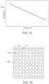
- FIG. 1C illustrates the ion beam profile 106 of the ion beam 116, according to one embodiment.
- the intensity of the ion beam profile 106 varies with the position within the cross-section of the ion beam 116.
- the depth of the gratings created by the ion beam is variable.
- the ion beam profile illustrated in FIG. 1C is linear, other variations of the ion beam profile are contemplated.
- the ion beam profile 106 is uniform, i.e., the intensity is uniform across the entire ion beam profile 106.
- the ion beam profile 106 is not uniform, i.e., the intensity is not uniform across the entire ion beam profile 106.
- the ion beam profile can also be a two-dimensional (2D) pattern.
- the ion beam profile 106 of the first ion beam is provided by filtering ions of the first ion beam with a plate having a plurality of filters.
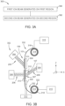
- FIG. 1D illustrates a plate 108 having a plurality of filters 110, according to one embodiment.
- the plate 108 is configured to interface with and couple to the ion source to modulate the intensity or distribution of the ion beam passing through the plate 108.
- the plurality of filters 110 includes portions 112 having the same or different diameters 114.
- the plurality of filters 110 can include holes, or openings, which allow ions of a desired intensity and/or density to pass therethrough.
- the plate 108 is fabricated from a material of sufficient thickness which is resistant or inert to ion beam bombardment and prevents ions from passing threrethrough.
- the plurality of filters 110 extend through the plate 108 to form openings through which the ion beam passes.
- the plurality of filters 110 are illustrated as being substantially circle-shaped with an approximately even distribution between adjacent filters of the first plurality of filters. However, any number, shape, orientation, spacing, or arrangement of the plurality of filters 110 can be utilized to modulate the intensity or distribution of the ion beam passing therethrough to create the desired ion beam profile.
- the ion beam profile 106 is provided by changing to a plasma profile of the first ion beam.
- the first device area 102 is exposed to the first ion beam for a first period of time to form a first plurality of gratings of the first device 104.
- the substrate 101 is repeatedly moved, i.e., stepped, such that each first device area 102 is exposed to the first ion beam 116 with the ion beam profile 106.
- a second ion beam is projected onto a second portion of a substrate.
- the second portion includes a second device area 120 of the substrate 101, according to one embodiment.
- the second ion beam has a second beam area corresponding to the second device area 120.
- the second device area 120 corresponds to each second device of a plurality of second devices 122 to be formed in the grating material 103.
- the second ion beam is projected to the second device area 120 with a ion beam profile 106 as described herein.
- the ion beam profile of the second ion beam can be different or the same as the ion beam profile of the first ion beam.
- the second device area 120 is exposed to the second ion beam for a second period of time to form a second plurality of gratings of the second device 122.
- the first period of time may partially overlap with the second period of time, and thus a portion of operation 190 may overlap with operation 192, according to one embodiment.
- the substrate 101 is repeatedly moved, i.e., stepped, such that each second device area 120 is exposed to the second ion beam with the ion beam profile.
- a third ion beam is projected onto a third portion of a substrate.
- the third portion includes a third device area 124 of the substrate 101, according to one embodiment.
- the third ion beam has a third beam area corresponding to the third device area 124.
- the third device area 124 corresponds to each third device of a plurality of third devices 126 to be formed in the grating material 103.
- the third ion beam is projected to the third device area 124 with a ion beam profile 106 as described herein.
- the ion beam profile of the third ion beam can be different or the same as the ion beam profile of the first and/or ion beam.
- the third device area 124 is exposed to the third ion beam for a third period of time to form a third plurality of gratings of the second device 122.
- the substrate 101 is repeatedly moved, i.e., stepped, such that each third device area 124 is exposed to the third ion beam with the ion beam profile.
- at least one of the first ion beam profile, the second ion beam profile, and the third ion beam profile is not uniform.
- the first period of time may partially overlap with the third period of time, and thus at least a portion of operation 190 may overlap with operation 194, according to one embodiment.
- the second period of time may partially overlap with the third period of time, and thus a portion of operation 192 may overlap with operation 194, according to one embodiment.
- the first period of time may partially overlap with the second period of time and the third period of time, and thus a portion of operation 190 may overlap with operations 192, 194, according to one embodiment.
- FIG. 2A is a flow diagram of method 200 operations for forming gratings, according to one embodiment. Although the method 200 operations are described in conjunction with FIGs. 2A -2F, persons skilled in the art will understand that any system configured to perform the method operations, in any order, falls within the scope of the embodiments described herein.
- the method 200 begins at operation 290, where a first portion of a substrate is exposed to an ion beam from an ion source.
- FIG. 2B illustrates an ion beam 206 incident on a first region a 1 of the substrate 101, according to one embodiment.
- An ion source 202 projects the ion beam 206 to the first region a 1 .
- the ion source 202 has a plurality of angled segments 204 configured to project the ion beams 206 generated by the ion source to the substrate 101, i.e., the ion source 202 is a segmented ion source.
- the ion beams 206 projected to the substrate 101 have at least one beam angle ⁇ 1 relative to a surface 105 of the substrate 101.
- the angled segments 204 can be localized to regions of waveguide combiners fabricated by the method 100, for example, the first device areas 102, the second device areas 120, and the third device areas 124.
- the substrate 101 is disposed in a first position G1.
- a first plurality of gratings 212 is formed from, or in, the grating material 103.
- the first plurality of gratings 212 have a slant angle ⁇ 1 that is defined between a first direction parallel to the surface 105 and a second direction perpendicular to the surface.
- the slant angle ⁇ 1 is about equal to the beam angle ⁇ 1 .
- the slant angle ⁇ 1 and/or beam angle ⁇ 1 can vary from about 5° to about 175°.
- a patterned hardmask 213 is disposed over the grating material 103.
- the ion beam 206 contacts exposed portions of the grating material and etches gratings in the grating material 103.
- the ion beams 206 projected to the substrate 101 have a plurality of different beam angles ⁇ corresponding to a rolling k-vector 210 such that portions of a plurality of gratings have different slant angles ⁇ relative to the surface normal 105.
- FIG. 2C illustrates an ion beam 206 incident on a second portion a 2 of the substrate 101, according to one embodiment.
- a vertical distance 208 of the substrate 101 from the segmented ion source 202 changes.
- the substrate 101 can be moved by a pedestal (not shown) disposed under the substrate 101.
- the ion source 202 is moved in a vertical direction (e.g., perpendicular to the surface of the substrate 101), and/or in a horizontal direction (e.g., parallel to the surface of the substrate 101).
- the ion source 202 is moved from the first positon G1, where the first portion a 1 of the grating material 103 is exposed, to a second positon G2, where the second portion a 2 of the grating material is exposed.
- a second plurality of gratings 218 is formed from, or in, the grating material 103.
- the second plurality of gratings 218 has a slant angle ⁇ 2 that is defined between the first direction parallel to the surface 105 and the second direction perpendicular to the surface.
- the slant angle ⁇ 2 is about equal to the beam angle ⁇ 2 .
- the slant angle ⁇ 2 and/or beam angle ⁇ 1 can vary from about 5° to about 175°.
- the first slant angle ⁇ 1 is from about 5° to about 85°
- the second slant angle ⁇ 2 is from about 95° to about 175°, according to one embodiment.
- a profile for a plurality of gratings includes the variance in depths between individual grating elements, the variance in angles between individual grating elements, and the rate of change of the angles and/or depths between individual grating elements.
- FIG. 2D illustrates a plurality of gratings 280 with a sloped profile 216, according to one embodiment. Smoothly scanning the substrate 101 from the first position G1 to the second position G2 can form a plurality of gratings 280 with a plurality of depths 214 having the sloped profile 216.
- the ion beam profile 106 of the ion beam 206 also can create a profile in the plurality of gratings. Either, or both, of the first or second plurality of gratings 212, 218 can have the sloped profile 216.
- FIG. 2E illustrates a plurality of gratings 280 with a stepped profile 222, according to one embodiment. Stepping the substrate 101 from the first position G1 to the second position G2 form the plurality of gratings 280 with a plurality of depths 214 having the stepped profile 222.
- the ion beam profile 106 of the ion beam 206 also can create a profile in the plurality of gratings. Either, or both, of the first or second plurality of gratings 212, 218 can have the stepped profile 222.
- the first plurality of gratings 212 has a sloped profile 216. In one embodiment, the first plurality of gratings 212 has a stepped profile 222. In one embodiment, the first plurality of gratings 212 has a first profile, and the second plurality of gratings 218 has a different profile.
- the patterned hardmask 213 has a thickness that filters ion beams 206 having the plurality of different beam angles ⁇ such that each of the plurality of gratings 212, 218 have the same slant angles ⁇ 1 , ⁇ 2 .
- at least one of the gratings in one or more of the plurality of gratings 212, 218 has a different slant angle ⁇ 1 , ⁇ 2 than one of the other gratings in the same plurality of gratings.
- at least one of the first ion beam profile and the second ion beam profile is not uniform.
- FIG. 3A is a flow diagram of method 300 operations for forming gratings, according to one embodiment. Although the method 300 operations are described in conjunction with FIGs. 3A-3C , persons skilled in the art will understand that any system configured to perform the method operations, in any order, falls within the scope of the embodiments described herein.
- the method 300 begins at operation 390, where a first portion of a flexible substrate is exposed to an ion beam with a first ion beam profile.
- FIG. 3B illustrates an angled etch system 302, according to one embodiment.
- the angled etch system 302 is configured expose ion beams 206 at different angles onto the substrate 101.
- the angled etch system 302 includes a pedestal 304, a plurality of ion beam chambers 306, a scanner 312, and a rolling system 322.
- the pedestal 304 retains the substrate 101 such that a first surface 107 of the substrate 101 is exposed to ion beams 206 generated by one or more ion beam chambers 306 oriented toward the first surface 107.
- the pedestal 304 has one or more holes 307 to allow one or more ion beam 206 to pass therethrough and form one more devices 310 on the first surface 107.
- a second surface 109 of the substrate 101 is exposed to the one or more ion beams 206 generated by the one or more ion beam chambers 306 oriented toward the second surface 109.
- the first surface 107 and the second surface 109 are exposed to the ion beam 206 to form devices 310 on the first surface 107 and the second surface 109.
- the angled etch system 302 is configured to create one or more devices 310 on both surfaces 107, 109 of the substrate 101.
- Each of the devices 310 has a plurality of gratings having slant angles (e.g., the plurality of gratings 212, 218).
- the angled etch system 302 can include the scanner 312 operable to move the pedestal 304 along at least one of a y-direction and an x-direction.
- the substrate 101 has rollable and flexible properties such that the rolling system 322 is configured to position a first segment 316 of the substrate 101 in the path of the ion beam 206 to form the devices 310.
- the rolling system 322 includes a plurality of rollers 314 and a plurality of roller actuators 315.
- the rollers 314 rotate rolled portions 318 of the flexible substrate 101, so that additional portions 332 of the substrate can be exposed to the plurality of ion beam chambers.
- Each of the roller actuators 315 are configured to rotate one of the plurality of rollers 314 to expose different portions of the substrate 101 to the ion beam chambers 306.
- FIG. 3C illustrates an angled etch system 302', according to one embodiment.
- the angled etch system 302' includes a rolling system 322' and one or more ion beam chambers 306.
- the ion beam chambers 306 are located on the same side 107 of the substrate 101.
- the angled etch system 322' includes a stabilizing member 330, a plurality of rollers 314, and a plurality of roller actuators 315.
- the rollers 314 rotate rolled portions 318 of the flexible substrate 101, so that additional portions 332 of the substrate can be exposed to the plurality of ion beam chambers.
- the substrate 101 is rolled along the supporting member 330.
- Each of the roller actuators 315 are configured to rotate one of the plurality of rollers 314 to expose different portions of the substrate 101 to the ion beam chambers 306.
- a second portion of the flexible substrate is exposed to an ion beam with a second ion beam profile.
- the first and second ion beam profiles can be the same or different. In some embodiments, at least one of the first ion beam profile and the second ion beam profile is not uniform.
- additional portions 332 of the substrate 101 are exposed to the plurality of ion beam chambers. For example, the rolling system 322, 322' advance the additional portions 332 of the substrate 101 to be exposed to the plurality of ion beam chambers 306.
- angled etch systems 302, 302' can be used in any of the methods 100, 200, 300, 400 disclosed herein.
- FIG. 4A is a flow diagram of method 400 operations for forming gratings, according to an embodiment of the claimed invention. Although the method 400 operations are described in conjunction with FIGs. 4A-4C , persons skilled in the art will understand that any system configured to perform the method operations, in any order, falls within the scope of the embodiments described herein.
- the method 400 begins at operation 490, where a resist material is deposited on a grating material.
- FIG. 4B illustrates the substrate 101 with a resist material 404 disposed over the grating material 103, according to one embodiment.
- the portion of the material illustrated in FIGs. 4B-4E is the first device area 102, the second device area 120, or the third device area 124 described above.
- the resist material 404 can be any resist material used in the art, such as, but not limited to, a photoresist, a liquid resist, and the like.
- a patterned hardmask 213 is disposed over the grating material 103 and under the resist material 404.
- FIG. 4C illustrates the substrate 101 with a resist layer 402 disposed over the grating material 103, according to one embodiment.
- Operation 492 includes forming the resist material 404 into a resist layer 402 having a first portion of pattern features 406 having a first slant angle ⁇ 1 , and a second portion of pattern features 408 having a second slant angle ⁇ 2 .
- the first portion of pattern features 406 is formed over the first region a 1
- the second portion of pattern features 408 is formed over the second region a 2 , according to some embodiments.
- the resist layer 402 is formed by a nanoimprint lithography process by pressing a mold against the resist material 404. Heat is applied to the resist material 404 during operation 492, according to one embodiment. Ultraviolet light (UV) is applied to the resist material 404 during operation 492, according to one embodiment.
- the resist material 404 includes a photoresist, and the resist layer 402 is formed by a photolithography process.
- FIG. 4D illustrates the substrate 101 exposed to the ion beam 206, according to one embodiment.
- the first portion of pattern features 406 of the resist layer 402 has a slant angle ⁇ 1 that is defined between a first direction parallel to a surface 405 of the substrate 101 and a second direction perpendicular to the surface 405.
- the slant angle ⁇ 1 is about equal to a first beam angle ⁇ 1 of the ion beam, such that the ion beam etches the first plurality of gratings 212 having the slant angle ⁇ 1 in the grating material 103 on the first region a 1 of the substrate 101.
- the second portion of pattern features 408 of the resist layer 402 have a second slant angle ⁇ 2 such that the ion beam 206 having the first beam angle ⁇ 1 does not etch the grating material 103 on the second region a 2 of the substrate 101.
- the slant angle ⁇ 1 can vary from about 5° to about 175°.
- a second region of a substrate is exposed to an ion beam with a second ion beam profile.
- the first and second ion beam profiles can be the same or different. In some embodiments, at least one of the first ion beam profile and the second ion beam profile is not uniform.
- FIG. 4E illustrates the substrate 101 exposed to the ion beam 206, according to one embodiment.
- the second portion of pattern features 408 of the resist layer 402 has a slant angle ⁇ 2 that is defined between the first direction parallel to a surface 405 of the substrate 101 and the second direction perpendicular to the surface 405.
- the first portion of pattern features 406 of the resist layer 402 have the first slant angle ⁇ 1 , such that the ion beam 206 having a second beam angle ⁇ 2 does not etch the grating material 103 on the first region a 1 of the substrate 101.
- the second portion of pattern features 408 of the resist layer 402 have the second slant angle ⁇ 2 such that the ion beam 206 having the second beam angle ⁇ 2 etches the grating material 103 on the second region a 2 of the substrate 101.
- the slant angle ⁇ 1 can vary from about 5° to about 175°.
- the first slant angle ⁇ 1 is from about 5° to about 85°
- the second slant angle ⁇ 2 is from about 95° to about 175°, according to one embodiment.
- One or more waveguide combiners 128 can be formed from the methods 100, 200, 300, 400.
- the waveguide combiner 128 includes one of the first devices 104 having the first plurality of gratings, one of the second devices 122 having the plurality of gratings, and one of the third devices 126 having the third plurality of gratings, according to one embodiment.
- the method includes depositing a resist material on a grating material disposed over a substrate, patterning the resist material into a resist layer, projecting a first ion beam to the first device area to form a first plurality of gratings, and projecting a second ion beam to the second device area to form a second plurality of gratings.
- a patterned resist layer allows for projecting an ion beam over a large area, which is often easier than focusing the ion beam in a specific area.
- the angles of elements the patterned resist facilitates ion etching for angles of the ion beam that are similar to angles of the elements of the patterned resist layer. Other regions are less patterned, due to the mismatch of the angles of the ion beam to the angles of the elements of the patterned resist layer.
Landscapes
- Physics & Mathematics (AREA)
- Chemical & Material Sciences (AREA)
- Engineering & Computer Science (AREA)
- General Physics & Mathematics (AREA)
- Optics & Photonics (AREA)
- Mechanical Engineering (AREA)
- Manufacturing & Machinery (AREA)
- Organic Chemistry (AREA)
- Chemical Kinetics & Catalysis (AREA)
- Materials Engineering (AREA)
- Metallurgy (AREA)
- Analytical Chemistry (AREA)
- Health & Medical Sciences (AREA)
- Plasma & Fusion (AREA)
- Toxicology (AREA)
- Ophthalmology & Optometry (AREA)
- Crystallography & Structural Chemistry (AREA)
- Diffracting Gratings Or Hologram Optical Elements (AREA)
- Micromachines (AREA)
- Drying Of Semiconductors (AREA)
Claims (10)
- Procédé de formation de réseaux, comprenant :le dépôt d'un matériau de réserve sur un matériau de réseau (490) disposé sur un substrat, le matériau de réserve comportant une première zone de dispositif et une seconde zone de dispositif ;la structuration du matériau de réserve en une couche de réserve structurée (492), la couche de réserve structurée comportant :une première partie des caractéristiques de structure formée sur la première zone de dispositif, la première partie des caractéristiques de la structure comportant un premier angle d'inclinaison ;une seconde partie de structure formée sur la seconde zone de dispositif, la seconde partie de structure comportant un second angle d'inclinaison ; la projection d'un premier faisceau d'ions sur la première zone de dispositif pendant une première période de temps pour former une première pluralité de réseaux dans le matériau de réseau (490),le premier faisceau d'ions comportant un premier angle de faisceau par rapport à une surface du substrat, le premier faisceau d'ions comportant un premier profil de faisceau d'ions,dans lequel le premier angle d'inclinaison est à peu près égal au premier angle de faisceau du premier faisceau d'ions, tandis que la seconde partie des caractéristiques de structure comporte le second angle d'inclinaison, de sorte que le faisceau d'ions comportant le premier angle de faisceau ne forme pas de réseaux sur la seconde zone de dispositif du substrat ; etla projection d'un second faisceau d'ions sur la seconde zone de dispositif pendant une seconde période de temps pour former une seconde pluralité de réseaux dans le matériau du réseau (492),le second faisceau d'ions comportant un second angle de faisceau par rapport à la surface du substrat, le second faisceau d'ions comportant un second profil de faisceau d'ions, dans lequel la première partie des caractéristiques de structure comporte le premier angle d'inclinaison, de sorte que le faisceau d'ions comportant le second angle de faisceau ne forme pas de réseaux sur la première zone de dispositif du substrat ;dans lequel au moins l'un du profil du premier faisceau d'ions et du second faisceau d'ions n'est pas uniforme.
- Procédé selon la revendication 1, dans lequella première pluralité de réseaux comporte un premier profil,la seconde pluralité de réseaux comporte un second profil, etle premier profil est différent du second profil.
- Procédé selon la revendication 2, dans lequel le premier profil est un profil étagé.
- Procédé selon la revendication 2, dans lequel le premier profil est un profil incliné.
- Procédé selon la revendication 1, dans lequelle premier angle est compris entre environ 5 ° et environ 85 °, etle second angle est compris entre environ 95 ° et environ 175 °.
- Procédé selon la revendication 1, en particulier pour former une ou plusieurs pluralités de réseaux, dans lequel la structuration comprend la pression d'un masque contre le matériau de réserve.
- Procédé selon la revendication 6, dans lequella première pluralité de réseaux comporte un premier profil,la seconde pluralité de réseaux comporte un second profil, etle premier profil est différent du second profil.
- Procédé selon la revendication 6, dans lequel la structuration du matériau de réserve comprend l'exposition du matériau de réserve à la lumière ultraviolette (UV).
- Procédé selon la revendication 6, dans lequel la structuration du matériau de réserve comprend le chauffage du matériau de réserve.
- Procédé selon la revendication 1, dans lequel la projection du premier faisceau d'ions comprend le filtrage d'ions du premier faisceau d'ions avec une plaque comportant une pluralité de filtres.
Applications Claiming Priority (2)
| Application Number | Priority Date | Filing Date | Title |
|---|---|---|---|
| US201862780792P | 2018-12-17 | 2018-12-17 | |
| PCT/US2019/066599 WO2020131733A1 (fr) | 2018-12-17 | 2019-12-16 | Procédé de formation de réseaux |
Publications (3)
| Publication Number | Publication Date |
|---|---|
| EP3899645A1 EP3899645A1 (fr) | 2021-10-27 |
| EP3899645A4 EP3899645A4 (fr) | 2022-09-14 |
| EP3899645B1 true EP3899645B1 (fr) | 2024-11-20 |
Family
ID=83998641
Family Applications (1)
| Application Number | Title | Priority Date | Filing Date |
|---|---|---|---|
| EP19900530.7A Active EP3899645B1 (fr) | 2018-12-17 | 2019-12-16 | Procédé de formation de réseaux |
Country Status (7)
| Country | Link |
|---|---|
| US (1) | US11512385B2 (fr) |
| EP (1) | EP3899645B1 (fr) |
| JP (1) | JP7483711B2 (fr) |
| KR (1) | KR102793797B1 (fr) |
| CN (1) | CN113168020B (fr) |
| TW (1) | TWI866941B (fr) |
| WO (1) | WO2020131733A1 (fr) |
Families Citing this family (9)
| Publication number | Priority date | Publication date | Assignee | Title |
|---|---|---|---|---|
| JP2023534997A (ja) * | 2020-07-22 | 2023-08-15 | アプライド マテリアルズ インコーポレイテッド | 深さが変化する屈折率膜の堆積のための方法 |
| WO2022233918A1 (fr) * | 2021-05-06 | 2022-11-10 | Nil Technology Aps | Fabrication de réseaux optiques à l'aide d'une photorésine profilée sur la base d'une lithographie à échelle de gris |
| FI130664B1 (fi) * | 2021-05-17 | 2024-01-09 | Dispelix Oy | Menetelmä porrastetun hilan valmistamiseksi |
| WO2023064095A1 (fr) * | 2021-10-15 | 2023-04-20 | Applied Materials, Inc. | Réseau partiellement métallisé en tant qu'incoupleur de guide d'ondes à haute performance |
| JP7665204B2 (ja) * | 2021-10-21 | 2025-04-21 | 株式会社オプトラン | 光学用具の製造方法 |
| WO2023122426A1 (fr) * | 2021-12-22 | 2023-06-29 | Applied Materials, Inc. | Procédé de formation de dispositifs optiques à profondeurs multiples |
| CN114089470B (zh) * | 2022-01-20 | 2022-05-06 | 深圳珑璟光电科技有限公司 | 一种全息光波导及其制作装置、近眼显示设备 |
| US11828984B2 (en) * | 2022-02-24 | 2023-11-28 | Globalfoundries U.S. Inc. | Thermal management of an optical component for temperature control |
| US20260050110A1 (en) * | 2024-08-16 | 2026-02-19 | Tokyo Electron Limited | Method for angled feature formation |
Family Cites Families (17)
| Publication number | Priority date | Publication date | Assignee | Title |
|---|---|---|---|---|
| JPH08129982A (ja) * | 1994-10-31 | 1996-05-21 | Hitachi Ltd | イオン源 |
| JP2005004068A (ja) | 2003-06-13 | 2005-01-06 | Dainippon Printing Co Ltd | スラント凹凸パターンの形成方法及びスラント凹凸パターンを有する基板 |
| JP3887356B2 (ja) * | 2003-07-08 | 2007-02-28 | エスアイアイ・ナノテクノロジー株式会社 | 薄片試料作製方法 |
| JP4012526B2 (ja) * | 2004-07-01 | 2007-11-21 | Tdk株式会社 | 薄膜コイルおよびその製造方法、ならびにコイル構造体およびその製造方法 |
| JP2006344527A (ja) | 2005-06-09 | 2006-12-21 | Tdk Corp | イオン源 |
| US8466953B2 (en) * | 2006-06-02 | 2013-06-18 | Nokia Corporation | Stereoscopic exit pupil expander display |
| JP5205866B2 (ja) | 2007-08-23 | 2013-06-05 | 住友電気工業株式会社 | モールドの形成方法、回折格子の形成方法、および分布帰還型半導体レーザの製造方法 |
| US8508848B2 (en) | 2007-12-18 | 2013-08-13 | Nokia Corporation | Exit pupil expanders with wide field-of-view |
| TWI416220B (zh) * | 2009-03-18 | 2013-11-21 | Wintek Corp | 光繞射元件及具有該光繞射元件的背光模組及顯示裝置 |
| CN101923282B (zh) * | 2009-06-09 | 2012-01-25 | 清华大学 | 纳米压印抗蚀剂及采用该纳米压印抗蚀剂的纳米压印方法 |
| JP5724213B2 (ja) * | 2010-05-13 | 2015-05-27 | セイコーエプソン株式会社 | 検出装置 |
| CN102323634B (zh) * | 2011-10-19 | 2016-06-22 | 苏州大学 | 一种全息双闪耀光栅的制作方法 |
| CN102540300A (zh) | 2012-02-16 | 2012-07-04 | 苏州大学 | 一种凸面双闪耀光栅的制备方法 |
| US20160035539A1 (en) | 2014-07-30 | 2016-02-04 | Lauri SAINIEMI | Microfabrication |
| US20160033784A1 (en) * | 2014-07-30 | 2016-02-04 | Tapani Levola | Optical Components |
| US10436958B2 (en) | 2016-10-05 | 2019-10-08 | Magic Leap, Inc. | Fabricating non-uniform diffraction gratings |
| CN106842397B (zh) * | 2017-01-05 | 2020-07-17 | 苏州苏大维格光电科技股份有限公司 | 一种树脂全息波导镜片及其制备方法、及三维显示装置 |
-
2019
- 2019-12-16 JP JP2021533795A patent/JP7483711B2/ja active Active
- 2019-12-16 KR KR1020217022392A patent/KR102793797B1/ko active Active
- 2019-12-16 US US16/715,906 patent/US11512385B2/en active Active
- 2019-12-16 EP EP19900530.7A patent/EP3899645B1/fr active Active
- 2019-12-16 WO PCT/US2019/066599 patent/WO2020131733A1/fr not_active Ceased
- 2019-12-16 CN CN201980081016.0A patent/CN113168020B/zh active Active
- 2019-12-17 TW TW108146180A patent/TWI866941B/zh active
Also Published As
| Publication number | Publication date |
|---|---|
| JP7483711B2 (ja) | 2024-05-15 |
| CN113168020B (zh) | 2023-08-25 |
| JP2022513850A (ja) | 2022-02-09 |
| CN113168020A (zh) | 2021-07-23 |
| TWI866941B (zh) | 2024-12-21 |
| WO2020131733A1 (fr) | 2020-06-25 |
| EP3899645A1 (fr) | 2021-10-27 |
| KR20210094120A (ko) | 2021-07-28 |
| US11512385B2 (en) | 2022-11-29 |
| KR102793797B1 (ko) | 2025-04-08 |
| TW202037933A (zh) | 2020-10-16 |
| US20200192010A1 (en) | 2020-06-18 |
| EP3899645A4 (fr) | 2022-09-14 |
Similar Documents
| Publication | Publication Date | Title |
|---|---|---|
| EP3899645B1 (fr) | Procédé de formation de réseaux | |
| US12591174B2 (en) | Microlithographic fabrication of structures | |
| KR102611648B1 (ko) | 광학적 격자 컴포넌트 및 이를 형성하는 방법 | |
| US11766744B2 (en) | Method of forming a plurality of gratings | |
| KR102778504B1 (ko) | 가변 깊이 디바이스 구조들을 형성하는 방법들 | |
| CN116490806B (zh) | 用于制造光学器件结构的方法 | |
| CN115427845B (zh) | 形成光学器件的方法 | |
| US20210286132A1 (en) | Forming variable depth structures with laser ablation | |
| US12153344B2 (en) | Lithography method to form structures with slanted angle | |
| US20230375774A1 (en) | Method for roughness reduction in manufacturing optical device structures |
Legal Events
| Date | Code | Title | Description |
|---|---|---|---|
| STAA | Information on the status of an ep patent application or granted ep patent |
Free format text: STATUS: THE INTERNATIONAL PUBLICATION HAS BEEN MADE |
|
| PUAI | Public reference made under article 153(3) epc to a published international application that has entered the european phase |
Free format text: ORIGINAL CODE: 0009012 |
|
| STAA | Information on the status of an ep patent application or granted ep patent |
Free format text: STATUS: REQUEST FOR EXAMINATION WAS MADE |
|
| 17P | Request for examination filed |
Effective date: 20210705 |
|
| AK | Designated contracting states |
Kind code of ref document: A1 Designated state(s): AL AT BE BG CH CY CZ DE DK EE ES FI FR GB GR HR HU IE IS IT LI LT LU LV MC MK MT NL NO PL PT RO RS SE SI SK SM TR |
|
| DAV | Request for validation of the european patent (deleted) | ||
| DAX | Request for extension of the european patent (deleted) | ||
| A4 | Supplementary search report drawn up and despatched |
Effective date: 20220812 |
|
| RIC1 | Information provided on ipc code assigned before grant |
Ipc: G02B 5/18 20060101ALN20220808BHEP Ipc: H01J 37/305 20060101ALI20220808BHEP Ipc: G02B 30/00 20200101ALI20220808BHEP Ipc: G02B 27/01 20060101ALI20220808BHEP Ipc: G02B 27/42 20060101AFI20220808BHEP |
|
| GRAP | Despatch of communication of intention to grant a patent |
Free format text: ORIGINAL CODE: EPIDOSNIGR1 |
|
| STAA | Information on the status of an ep patent application or granted ep patent |
Free format text: STATUS: GRANT OF PATENT IS INTENDED |
|
| RIC1 | Information provided on ipc code assigned before grant |
Ipc: G02B 6/00 20060101ALN20240514BHEP Ipc: G02B 3/00 20060101ALN20240514BHEP Ipc: B26D 11/00 20060101ALN20240514BHEP Ipc: G02B 5/18 20060101ALN20240514BHEP Ipc: C23C 14/56 20060101ALI20240514BHEP Ipc: C23C 14/54 20060101ALI20240514BHEP Ipc: C23C 14/22 20060101ALI20240514BHEP Ipc: H01J 37/305 20060101ALI20240514BHEP Ipc: G02B 30/00 20200101ALI20240514BHEP Ipc: G02B 27/01 20060101ALI20240514BHEP Ipc: G02B 27/42 20060101AFI20240514BHEP |
|
| RIC1 | Information provided on ipc code assigned before grant |
Ipc: G02B 6/00 20060101ALN20240603BHEP Ipc: G02B 3/00 20060101ALN20240603BHEP Ipc: B26D 11/00 20060101ALN20240603BHEP Ipc: G02B 5/18 20060101ALN20240603BHEP Ipc: C23C 14/56 20060101ALI20240603BHEP Ipc: C23C 14/54 20060101ALI20240603BHEP Ipc: C23C 14/22 20060101ALI20240603BHEP Ipc: H01J 37/305 20060101ALI20240603BHEP Ipc: G02B 30/00 20200101ALI20240603BHEP Ipc: G02B 27/01 20060101ALI20240603BHEP Ipc: G02B 27/42 20060101AFI20240603BHEP |
|
| INTG | Intention to grant announced |
Effective date: 20240618 |
|
| GRAS | Grant fee paid |
Free format text: ORIGINAL CODE: EPIDOSNIGR3 |
|
| GRAA | (expected) grant |
Free format text: ORIGINAL CODE: 0009210 |
|
| STAA | Information on the status of an ep patent application or granted ep patent |
Free format text: STATUS: THE PATENT HAS BEEN GRANTED |
|
| AK | Designated contracting states |
Kind code of ref document: B1 Designated state(s): AL AT BE BG CH CY CZ DE DK EE ES FI FR GB GR HR HU IE IS IT LI LT LU LV MC MK MT NL NO PL PT RO RS SE SI SK SM TR |
|
| REG | Reference to a national code |
Ref country code: GB Ref legal event code: FG4D |
|
| REG | Reference to a national code |
Ref country code: CH Ref legal event code: EP |
|
| REG | Reference to a national code |
Ref country code: DE Ref legal event code: R096 Ref document number: 602019062408 Country of ref document: DE |
|
| REG | Reference to a national code |
Ref country code: IE Ref legal event code: FG4D |
|
| REG | Reference to a national code |
Ref country code: LT Ref legal event code: MG9D |
|
| REG | Reference to a national code |
Ref country code: NL Ref legal event code: MP Effective date: 20241120 |
|
| PG25 | Lapsed in a contracting state [announced via postgrant information from national office to epo] |
Ref country code: PT Free format text: LAPSE BECAUSE OF FAILURE TO SUBMIT A TRANSLATION OF THE DESCRIPTION OR TO PAY THE FEE WITHIN THE PRESCRIBED TIME-LIMIT Effective date: 20250320 Ref country code: HR Free format text: LAPSE BECAUSE OF FAILURE TO SUBMIT A TRANSLATION OF THE DESCRIPTION OR TO PAY THE FEE WITHIN THE PRESCRIBED TIME-LIMIT Effective date: 20241120 Ref country code: IS Free format text: LAPSE BECAUSE OF FAILURE TO SUBMIT A TRANSLATION OF THE DESCRIPTION OR TO PAY THE FEE WITHIN THE PRESCRIBED TIME-LIMIT Effective date: 20250320 |
|
| PG25 | Lapsed in a contracting state [announced via postgrant information from national office to epo] |
Ref country code: FI Free format text: LAPSE BECAUSE OF FAILURE TO SUBMIT A TRANSLATION OF THE DESCRIPTION OR TO PAY THE FEE WITHIN THE PRESCRIBED TIME-LIMIT Effective date: 20241120 Ref country code: NL Free format text: LAPSE BECAUSE OF FAILURE TO SUBMIT A TRANSLATION OF THE DESCRIPTION OR TO PAY THE FEE WITHIN THE PRESCRIBED TIME-LIMIT Effective date: 20241120 |
|
| REG | Reference to a national code |
Ref country code: AT Ref legal event code: MK05 Ref document number: 1744103 Country of ref document: AT Kind code of ref document: T Effective date: 20241120 |
|
| PG25 | Lapsed in a contracting state [announced via postgrant information from national office to epo] |
Ref country code: BG Free format text: LAPSE BECAUSE OF FAILURE TO SUBMIT A TRANSLATION OF THE DESCRIPTION OR TO PAY THE FEE WITHIN THE PRESCRIBED TIME-LIMIT Effective date: 20241120 |
|
| PG25 | Lapsed in a contracting state [announced via postgrant information from national office to epo] |
Ref country code: ES Free format text: LAPSE BECAUSE OF FAILURE TO SUBMIT A TRANSLATION OF THE DESCRIPTION OR TO PAY THE FEE WITHIN THE PRESCRIBED TIME-LIMIT Effective date: 20241120 |
|
| PG25 | Lapsed in a contracting state [announced via postgrant information from national office to epo] |
Ref country code: NO Free format text: LAPSE BECAUSE OF FAILURE TO SUBMIT A TRANSLATION OF THE DESCRIPTION OR TO PAY THE FEE WITHIN THE PRESCRIBED TIME-LIMIT Effective date: 20250220 |
|
| PG25 | Lapsed in a contracting state [announced via postgrant information from national office to epo] |
Ref country code: AT Free format text: LAPSE BECAUSE OF FAILURE TO SUBMIT A TRANSLATION OF THE DESCRIPTION OR TO PAY THE FEE WITHIN THE PRESCRIBED TIME-LIMIT Effective date: 20241120 Ref country code: GR Free format text: LAPSE BECAUSE OF FAILURE TO SUBMIT A TRANSLATION OF THE DESCRIPTION OR TO PAY THE FEE WITHIN THE PRESCRIBED TIME-LIMIT Effective date: 20250221 Ref country code: LV Free format text: LAPSE BECAUSE OF FAILURE TO SUBMIT A TRANSLATION OF THE DESCRIPTION OR TO PAY THE FEE WITHIN THE PRESCRIBED TIME-LIMIT Effective date: 20241120 |
|
| PG25 | Lapsed in a contracting state [announced via postgrant information from national office to epo] |
Ref country code: PL Free format text: LAPSE BECAUSE OF FAILURE TO SUBMIT A TRANSLATION OF THE DESCRIPTION OR TO PAY THE FEE WITHIN THE PRESCRIBED TIME-LIMIT Effective date: 20241120 |
|
| PG25 | Lapsed in a contracting state [announced via postgrant information from national office to epo] |
Ref country code: RS Free format text: LAPSE BECAUSE OF FAILURE TO SUBMIT A TRANSLATION OF THE DESCRIPTION OR TO PAY THE FEE WITHIN THE PRESCRIBED TIME-LIMIT Effective date: 20250220 |
|
| PG25 | Lapsed in a contracting state [announced via postgrant information from national office to epo] |
Ref country code: SM Free format text: LAPSE BECAUSE OF FAILURE TO SUBMIT A TRANSLATION OF THE DESCRIPTION OR TO PAY THE FEE WITHIN THE PRESCRIBED TIME-LIMIT Effective date: 20241120 |
|
| PG25 | Lapsed in a contracting state [announced via postgrant information from national office to epo] |
Ref country code: DK Free format text: LAPSE BECAUSE OF FAILURE TO SUBMIT A TRANSLATION OF THE DESCRIPTION OR TO PAY THE FEE WITHIN THE PRESCRIBED TIME-LIMIT Effective date: 20241120 |
|
| PG25 | Lapsed in a contracting state [announced via postgrant information from national office to epo] |
Ref country code: EE Free format text: LAPSE BECAUSE OF FAILURE TO SUBMIT A TRANSLATION OF THE DESCRIPTION OR TO PAY THE FEE WITHIN THE PRESCRIBED TIME-LIMIT Effective date: 20241120 |
|
| PG25 | Lapsed in a contracting state [announced via postgrant information from national office to epo] |
Ref country code: RO Free format text: LAPSE BECAUSE OF FAILURE TO SUBMIT A TRANSLATION OF THE DESCRIPTION OR TO PAY THE FEE WITHIN THE PRESCRIBED TIME-LIMIT Effective date: 20241120 |
|
| PG25 | Lapsed in a contracting state [announced via postgrant information from national office to epo] |
Ref country code: SK Free format text: LAPSE BECAUSE OF FAILURE TO SUBMIT A TRANSLATION OF THE DESCRIPTION OR TO PAY THE FEE WITHIN THE PRESCRIBED TIME-LIMIT Effective date: 20241120 |
|
| PG25 | Lapsed in a contracting state [announced via postgrant information from national office to epo] |
Ref country code: CZ Free format text: LAPSE BECAUSE OF FAILURE TO SUBMIT A TRANSLATION OF THE DESCRIPTION OR TO PAY THE FEE WITHIN THE PRESCRIBED TIME-LIMIT Effective date: 20241120 |
|
| PG25 | Lapsed in a contracting state [announced via postgrant information from national office to epo] |
Ref country code: IT Free format text: LAPSE BECAUSE OF FAILURE TO SUBMIT A TRANSLATION OF THE DESCRIPTION OR TO PAY THE FEE WITHIN THE PRESCRIBED TIME-LIMIT Effective date: 20241120 |
|
| REG | Reference to a national code |
Ref country code: CH Ref legal event code: PL |
|
| PG25 | Lapsed in a contracting state [announced via postgrant information from national office to epo] |
Ref country code: LU Free format text: LAPSE BECAUSE OF NON-PAYMENT OF DUE FEES Effective date: 20241216 |
|
| REG | Reference to a national code |
Ref country code: DE Ref legal event code: R097 Ref document number: 602019062408 Country of ref document: DE |
|
| PG25 | Lapsed in a contracting state [announced via postgrant information from national office to epo] |
Ref country code: SE Free format text: LAPSE BECAUSE OF FAILURE TO SUBMIT A TRANSLATION OF THE DESCRIPTION OR TO PAY THE FEE WITHIN THE PRESCRIBED TIME-LIMIT Effective date: 20241120 |
|
| PG25 | Lapsed in a contracting state [announced via postgrant information from national office to epo] |
Ref country code: MC Free format text: LAPSE BECAUSE OF FAILURE TO SUBMIT A TRANSLATION OF THE DESCRIPTION OR TO PAY THE FEE WITHIN THE PRESCRIBED TIME-LIMIT Effective date: 20241120 |
|
| PLBE | No opposition filed within time limit |
Free format text: ORIGINAL CODE: 0009261 |
|
| STAA | Information on the status of an ep patent application or granted ep patent |
Free format text: STATUS: NO OPPOSITION FILED WITHIN TIME LIMIT |
|
| REG | Reference to a national code |
Ref country code: BE Ref legal event code: MM Effective date: 20241231 |
|
| PG25 | Lapsed in a contracting state [announced via postgrant information from national office to epo] |
Ref country code: BE Free format text: LAPSE BECAUSE OF NON-PAYMENT OF DUE FEES Effective date: 20241231 |
|
| PG25 | Lapsed in a contracting state [announced via postgrant information from national office to epo] |
Ref country code: FR Free format text: LAPSE BECAUSE OF NON-PAYMENT OF DUE FEES Effective date: 20250120 |
|
| PG25 | Lapsed in a contracting state [announced via postgrant information from national office to epo] |
Ref country code: CH Free format text: LAPSE BECAUSE OF NON-PAYMENT OF DUE FEES Effective date: 20241231 |
|
| 26N | No opposition filed |
Effective date: 20250821 |
|
| PG25 | Lapsed in a contracting state [announced via postgrant information from national office to epo] |
Ref country code: IE Free format text: LAPSE BECAUSE OF NON-PAYMENT OF DUE FEES Effective date: 20241216 |
|
| GBPC | Gb: european patent ceased through non-payment of renewal fee |
Effective date: 20250220 |
|
| PGFP | Annual fee paid to national office [announced via postgrant information from national office to epo] |
Ref country code: DE Payment date: 20251015 Year of fee payment: 7 |
|
| PG25 | Lapsed in a contracting state [announced via postgrant information from national office to epo] |
Ref country code: GB Free format text: LAPSE BECAUSE OF NON-PAYMENT OF DUE FEES Effective date: 20250220 |