EP3901612B1 - Capteur de matière particulaire intégré doté d'une cavité - Google Patents
Capteur de matière particulaire intégré doté d'une cavité Download PDFInfo
- Publication number
- EP3901612B1 EP3901612B1 EP20171192.6A EP20171192A EP3901612B1 EP 3901612 B1 EP3901612 B1 EP 3901612B1 EP 20171192 A EP20171192 A EP 20171192A EP 3901612 B1 EP3901612 B1 EP 3901612B1
- Authority
- EP
- European Patent Office
- Prior art keywords
- optical element
- particulate matter
- photodetector
- light
- substrate
- Prior art date
- Legal status (The legal status is an assumption and is not a legal conclusion. Google has not performed a legal analysis and makes no representation as to the accuracy of the status listed.)
- Active
Links
Images




Classifications
-
- G—PHYSICS
- G01—MEASURING; TESTING
- G01N—INVESTIGATING OR ANALYSING MATERIALS BY DETERMINING THEIR CHEMICAL OR PHYSICAL PROPERTIES
- G01N15/00—Investigating characteristics of particles; Investigating permeability, pore-volume or surface-area of porous materials
- G01N15/06—Investigating concentration of particle suspensions
-
- G—PHYSICS
- G01—MEASURING; TESTING
- G01N—INVESTIGATING OR ANALYSING MATERIALS BY DETERMINING THEIR CHEMICAL OR PHYSICAL PROPERTIES
- G01N15/00—Investigating characteristics of particles; Investigating permeability, pore-volume or surface-area of porous materials
- G01N15/02—Investigating particle size or size distribution
- G01N15/0205—Investigating particle size or size distribution by optical means
- G01N15/0211—Investigating a scatter or diffraction pattern
-
- G—PHYSICS
- G01—MEASURING; TESTING
- G01N—INVESTIGATING OR ANALYSING MATERIALS BY DETERMINING THEIR CHEMICAL OR PHYSICAL PROPERTIES
- G01N15/00—Investigating characteristics of particles; Investigating permeability, pore-volume or surface-area of porous materials
- G01N15/10—Investigating individual particles
- G01N15/14—Optical investigation techniques, e.g. flow cytometry
- G01N15/1456—Optical investigation techniques, e.g. flow cytometry without spatial resolution of the texture or inner structure of the particle, e.g. processing of pulse signals
-
- G—PHYSICS
- G01—MEASURING; TESTING
- G01N—INVESTIGATING OR ANALYSING MATERIALS BY DETERMINING THEIR CHEMICAL OR PHYSICAL PROPERTIES
- G01N15/00—Investigating characteristics of particles; Investigating permeability, pore-volume or surface-area of porous materials
- G01N15/10—Investigating individual particles
- G01N15/14—Optical investigation techniques, e.g. flow cytometry
- G01N15/1434—Optical arrangements
-
- G—PHYSICS
- G01—MEASURING; TESTING
- G01N—INVESTIGATING OR ANALYSING MATERIALS BY DETERMINING THEIR CHEMICAL OR PHYSICAL PROPERTIES
- G01N15/00—Investigating characteristics of particles; Investigating permeability, pore-volume or surface-area of porous materials
- G01N15/06—Investigating concentration of particle suspensions
- G01N15/075—Investigating concentration of particle suspensions by optical means
-
- G—PHYSICS
- G01—MEASURING; TESTING
- G01N—INVESTIGATING OR ANALYSING MATERIALS BY DETERMINING THEIR CHEMICAL OR PHYSICAL PROPERTIES
- G01N15/00—Investigating characteristics of particles; Investigating permeability, pore-volume or surface-area of porous materials
- G01N15/10—Investigating individual particles
- G01N15/14—Optical investigation techniques, e.g. flow cytometry
- G01N15/1434—Optical arrangements
- G01N2015/1447—Spatial selection
-
- G—PHYSICS
- G01—MEASURING; TESTING
- G01N—INVESTIGATING OR ANALYSING MATERIALS BY DETERMINING THEIR CHEMICAL OR PHYSICAL PROPERTIES
- G01N15/00—Investigating characteristics of particles; Investigating permeability, pore-volume or surface-area of porous materials
- G01N15/10—Investigating individual particles
- G01N15/14—Optical investigation techniques, e.g. flow cytometry
- G01N2015/1486—Counting the particles
Definitions
- the invention relates to a particulate matter sensor and to a particulate matter sensor module comprising the particulate matter sensor.
- PM Particulate matter
- PM refers to solid particles and/or liquid droplets in a fluid. PM may pose a health risk, e.g. when inhaled, or cause bad visibility called haze.
- Typical categories of PM are PM10 and PM2.5, i.e. particles with diameters of 10 um and 2.5 um, respectively, and smaller.
- PM sensor modules comprise a light source emitting light into a detection volume and a light detector detecting light scattered by particulate matter in the detection volume.
- Conventional PM sensor modules are built from discrete components, i.e. light source assemblies with laser diodes, optical elements, photodetectors, printed circuit boards (PCB), discrete amplifiers, microprocessors, and housings, etc. Air flow for sampling of particles is generated using a fan or alternatively a heater element.
- PM sensor modules are of macroscopic scale, i.e. having a dimension in the order of several centimeters.
- a reason for the form factor and size of conventional PM sensor modules is the discrete nature of used optoelectronic components, i.e. laser diode, optical element, mounting aid and photodetector.
- US20150153275A1 discloses the features of the preamble of claim 1, disclosing a PM sensor that comprises a light source and a light detector disposed adjacent to each other in a body portion.
- the light source emits light toward air that has been introduced into the body portion.
- An optical lens disposed on the light source focuses the emitted light. Scattered light is detected by the light detector.
- US20160025628A1 discloses a mobile device configured to sense particulate matter.
- a sensor in the mobile device comprises a light emitter and a light receiver arranged at an angle.
- CN106483051B discloses a mobile device for measuring the concentration of particulate matter. Light is emitted by a flash of the mobile device. Backscattered light is collected by a collecting lens, filtered and detected by a light detector.
- EP3225977 A1 discloses a PM detector using a single chip with an integrated light source and detector.
- a problem to be solved by embodiments of the present invention is to provide a small PM sensor, which in particular yields reliable high-quality measurements.
- the particulate matter sensor of claim 1 comprises the following elements:
- Such PM sensor can be built with a small form factor, i.e. smaller than 7 mm x 7 mm x 2 mm, in particular smaller than 5 mm x 5 mm x 1.6 mm. Also it can be integrated into a PM sensor module or a portable electronic device such as a smartphone or an internet-of-things things (IoT) device. Moreover, such PM sensor has the advantage of having a low consumption of electrical current, which again makes it well suited for integration into battery-driven devices.
- IoT internet-of-things things
- the PM sensor further comprises
- An amount of light scattered by PM in the detection volume and received by the at least one photodetector depends i.a. on the optical power of the light source. Hence it is of interest to quantify the optical power.
- the light source comprises a VCSEL since the optical power of VCSELs is usually not controlled because an exact optical power is irrelevant for applications like time-of-flight (TOF) measurements.
- TOF time-of-flight
- the PM sensor comprises a photodiode arranged adjacent to the optical element.
- the photodiode may be arranged in the cavity, e.g. on a wall of the cavity facing the optical element.
- the photodiode may be integrated in the substrate. In that case, the manufacturing process is simplified, e.g. in that the photodiode is formed during a regular CMOS processing.
- the photodiode is adapted to measure stray light from the optical element, i.e. light which does not leave the optical element towards the detection volume but is reflected or scattered into other directions, e.g. backwards. It has been found that an amount of stray light is indicative of, in particular proportional to, the optical power.
- the control unit is further electrically connected to the photodiode and adapted to determine an optical power of the light source from the stray light and to evaluate the physical quantity related to the PM dependent on the determined optical power.
- the control unit is adapted to control the light source dependent on the determined optical power.
- the PM sensor comprises a photodiode arranged in or adjacent to the cavity and adapted to measure spontaneous emission of the light source.
- VCSELs have been found to exhibit spontaneous emission of light on one or more side walls, i.e. one or more walls other than a main emission surface of the VCSEL. Further, it has been found that an amount of spontaneous emission is, again, indicative of, in particular proportional to, the optical power.
- the control unit is further electrically connected to the photodiode and adapted to determine an optical power of the light source from the measured spontaneous emission and to evaluate the physical quantity related to the PM dependent on the determined optical power. Alternatively or additionally, the control unit is adapted to control the light source dependent on the determined optical power.
- the photodiode is advantageously integrated in the substrate.
- the described embodiments facilitate more accurate measurements of the physical quantity related to the PM, in particular in case that the optical power of the light source is otherwise unknown, as e.g. with a VCSEL.
- the described PM sensor is optimized for a large detection volume, because the PM count is directly proportional to the detection volume as defined above.
- a PM particle needs to generate enough scattered light in the direction of the at least one photodetector such that a signal from the scattered light detected by the at least one photodetector is above the noise level, e.g. dark current noise.
- the volume for which this condition is fulfilled is called the detection volume.
- the light scattered from PM is approximately described by Mie theory. To explain the optimization of the detection volume, a further approximation may be helpful:
- the detection volume is i.a. limited by geometrical effects, such as a spreading of light emitted by a point source or scattered by a particle.
- the spreading causes an intensity of the light to diminish with distance d from the point source or, respectively, the scattering particle as 1/d ⁇ 2, corresponding to a growing surface of an outgoing spherical wave. This has implications for the design of the PM sensor in general and of the optical element in particular.
- the optical element focusses the light beam, e.g. in a focus or a focus region. Accordingly, the intensity of the light beam increases with distance 1 from the optical element up to the focus as l ⁇ 2, corresponding to the decreasing surface of a conical light beam. It can be seen that this effect of increasing intensity of light within the detection volume counteracts and, to a certain degree, balances the spreading effect of light scattered by PM particles as described above. In this way, the detection volume is maximized for a given light source and a given photodetector.
- the detection volume accordingly ranges from the optical element at least to the focus of the light beam.
- a distance l 0 between the optical element and the focus may be at least 1 mm.
- an optimum focus distance depends on a threshold value of the at least one photodetector for resolving particle scattered light against noise, and the optical power of the light source, and a numerical aperture of the optical element.
- the detection volume may even extend beyond the focus, e.g. to 1.2 or 1.5 times l 0 for large particles. In this way, the PM sensor is adapted to detect PM at least as far as 1.5 mm from the optical element.
- the optical element may be adapted to collimate the light beam, i.e. to shape the light beam such that different rays within the light beam are essentially parallel outside the cavity.
- the light intensity theoretically remains constant along the light beam under the assumptions of no scattering and no attenuation.
- a collimating optical element instead of a focussing optical element yields a large detection volume, e.g. up to 3 cm from the optical element.
- the optical element is situated in the same plane as the at least one photodetector or only slightly above or below as described before. Accordingly, the optical element may in one embodiment protrude from the plane of the at least one photodetector, or, in another embodiment, only slightly do so, e.g. by at maximum 0.6 mm. Also, it is advantageous that a thickness of the optical element perpendicular to the light beam is small, i.e. below 2 mm, in particular below 1 mm. In this way, a shadowing of the at least one photodetector from light scattered by PM particles near the optical element by the optical element can be prevented. In other words, the detection volume may be increased towards, or optimally up to, the optical element.
- a height of the cavity i.e. a distance between the light source and the optical element, is at least 0.25 mm, in particular at least 0.45 mm. This makes the PM sensor more robust against manufacturing errors such as slight deviations from optimal dimensions. Together with the above considerations concerning shadowing, this leads to the conclusion that the thickness of the optical element should advantageously be small.
- the substrate is arranged on top of a base substrate, which may e.g. be a carrier made from glass, semiconductor, ceramics, etc.
- a base substrate which may e.g. be a carrier made from glass, semiconductor, ceramics, etc.
- the cavity may be delimited by the optical element on the one side, and by the base substrate on the other side.
- the light source may be arranged on the base substrate and emit light in direction to the optical element.
- the optical element may comprise a refractive lens or a diffractive optical element.
- the optical element comprises an imprint polymer lens or an injection-moulded lens.
- a polymer lens is formed on a glass carrier substrate, in particular multiple polymer lenses are formed on the glass carrier substrate.
- the glass carrier substrate is then diced to form a single lens.
- the polymer lens together with the glass carrier substrate is then placed on the cavity.
- the polymer lens is arranged on a glass carrier substrate with a thickness of less than 1000 um, e.g. 800 um, in particular less than 600 um.
- the optical element comprises a metamaterial that is transparent for the light beam.
- the metamaterial comprises structures effectively shaping the light beam as a lens.
- Such an element is also known as a diffractive optical element, DOE.
- DOE diffractive optical element
- a membrane is manufactured from the substrate, e.g. in form of a thin layer, and e.g. by etching the substrate from a bottom side almost through an entire thickness of the substrate such that the membrane remains at the front side of the substrate covering the cavity.
- the structures shaping the light beam are manufactured, either by structuring the membrane e.g. by etching, or by applying the structures onto the membrane.
- a thickness of the metamaterial is less than 20 ⁇ m, in particular less than 10 um.
- a thin optical element in general, enables minimum shadowing of scattered light, thus providing a large detection volume.
- a thin optical element facilitates a minimum required distance between the optical element and the at least one photodetector while preventing shadowing. Also, it facilitates a small overall form factor of the PM sensor.
- Another aspect relating to the optical element concerns stray light leaving the optical element in other directions than the desired light beam, e.g. to the sides, in particular towards the at least one photodetector. If such stray light reaches the at least one photodetector, it significantly increases the noise level and thus decreases the signal-to-noise ratio of the PM sensor, hence effectively decreasing the detection volume.
- the PM sensor advantageously comprises a light barrier between the optical element and the at least one photodetector.
- the light barrier comprises a blackening or silvering of side walls of the optical element facing the at least one photodetector.
- the blackening or silvering comprises a selective coating only reacting with the carrier glass layer but not with the polymer lens described above.
- Silvering is understood as providing a reflective coating serving as light barrier, but not necessarily consisting of silver. Other materials barring light from passing may be used.
- the light barrier comprises an aperture between the optical element and the light source, e.g. a chromium aperture.
- the aperture may advantageously be placed on at least one of the top or bottom side of the glass substrate.
- Such light barrier allows to block the stray light from reaching the at least one photodetector. At the same time, the light beam passes the optical beam unhindered. Also, stray light leaving the optical element towards the cavity is largely unaffected, such that the above described method of quantifying the optical power of the light source remains feasible with such embodiments.
- the following disclosure relating the one or more photodetectors shall be considered to be disclosed in combination with the PM sensor, however, also outside the application in such PM sensor, i.e. independent from the PM sensor, rather as a photodetector device comprising a photodetector integrated in and/or arranged on a substrate, which may be a semiconductor substrate including CMOS metallization and dielectric layers on top of the semiconductor substrate.
- the at least one photodetector may be of any type of photodetector, it is advantageous that it is a silicon-based photodetector.
- Such photodetector may be manufactured in the same process steps, e.g. in CMOS process steps, as is preferably the control unit represented by electronic circuitry integrated into the preferred silicon substrate.
- Such photodetectors are simpler to handle during manufacturing and less costly than other semiconductor photodetectors. Thus they are well suited for manufacturing large numbers of PM sensors, e.g. for IoT devices.
- the one or more photodetectors are arranged on the substrate and/or are integrated in the substrate.
- the at least one photodetector comprises an array of photodetectors, i.e. multiple photodetectors e.g. arranged in a regular pattern. This is useful since it is desired that the at least one photodetector covers a large area, while at the same time minimizing the distance to the optical element.
- the array of photodetectors may be distributed around the optical element, in particular in a plane. As an example, four photodetectors are distributed in the plane of the optical element. Or, arrays of photodetector pixels are arranged on the substrate.
- the photodetector pixels each have a planar dimension of less than 1x1 mm 2 , preferably less than 0.5x0.5 mm 2 , and even more preferably less than 0.3x0.3 mm 2 .
- the same square measures apply in case of non-square shaped pixels, such as circular shaped pixels.
- the at least one photodetector should advantageously be as close as possible to the optical element. In this way, the optical path length from scattering particle within the detection volume to the at least one photodetector is minimized and thus the signal-to-noise ratio maximized.
- the PM sensor comprises an optical filter on the at least one photodetector.
- the optical filter covers a surface of the at least one photodetector opposite to the substrate.
- the optical filter filters out light and radiation outside a dominant wavelength band of the light source. In this way, a background rejection is achieved since spurious light or radiation events do not reach the at least one photodetector.
- the photodetectors are separated by an electrically conducting material, e.g. having the shape of a grid with the photodetectors being arranged in the vacancies of the grid, e.g. in form of tiles or pixels as already laid out above.
- the photodetectors may be separated by a metallization of the substrate.
- manufacturing the electrically conducting material may be integrated in the regular processing of the substrate, e.g. of the CMOS layer stack, wherein a top most metallization of the CMOS layer stack is manufactured such that it, and in particular its partitioning borders, serves as the electrically conducting material separating the photodetectors.
- Such electrically conducting material between the photodetectors may be grounded and thus acts as a Faraday cage, and may be exposed towards the measuring volume.
- the electrically conducting material is adapted to protect the photodetectors from electromagnetic interference, e.g. with other electronic devices in an environment of the PM sensor.
- the above ranges of the pixel dimensions accordingly define a distance between the metal-lizations and promote the shielding from electromagnetic interference.
- the at least one photodetector is partitioned into a first partition facing the detection volume and a second partition shielded from light scattered by PM in the detection volume.
- the two separate partitions may be used to detect and cancel signals in the photodetectors that are due only to unwanted electromagnetic interference but not to light scattered by PM in the detection volume.
- the control unit is adapted to perform a differential measurement of the first partition and the second partition. In particular, spurious effects of electromagnetic interference with the first partition and the second partition of the at least one photodetector are thereby cancelled.
- a PM sensor module comprises a housing and a flow channel arranged in the housing. Further, the PM sensor module comprises a fan or a heater arranged in the housing and adapted to move air through the flow channel as well as the PM sensor as described in any of the embodiments above or in one of the embodiments below, wherein the PM sensor is arranged in the housing such that a part of the flow channel coincides with the detection volume.
- Fig. 1 shows a schematic cut through a PM sensor according to an embodiment
- Fig. 2 shows a perspective view of the PM sensor.
- a cavity 5 is formed by a substrate 4 which in the following is also referred to as semiconductor chip 4.
- the base substrate 6 may also be part of the semiconductor chip 4.
- the cavity 5 preferably is formed from a bottom side of the substrate 5, and hence may also show inclined side walls as indicated by the dashed lines.
- a light source 1 is arranged in the cavity 5 on the bottom side, i.e. the side facing the base substrate 6. Examples for the light source 1 are a laser diode or a vertical-cavity surface-emitting laser (VCSEL).
- VCSEL vertical-cavity surface-emitting laser
- an optical element 2 is arranged, thus closing the cavity 5.
- photodetectors 3, e.g. photodiodes are arranged on the semiconductor chip 4 on two or more sides of the optical element 2.
- the optical element 2 and photodetectors 3 are arranged in essentially the same plane.
- the optical element 2 should not protrude by more than 1 mm above the plane defined by the photodetectors 3.
- the reason for this has been discussed above and is illustrated in Fig. 9 : A protruding lens 15 leads to a shadowing such that a scattered light pulse 10 scattered by a PM particle much closer to the lens 15 than particle 9 would not reach the photodetectors 3 and thus not be detected.
- an upper surface of the semiconductor chip 4 may comprise arrays of photodetectors 3, e.g. four arrays of photodetector pixels.
- Metallizations 18 are provided between or around the individual photodetector pixels.
- the metallizations 18 may be made of any electrically conducting material.
- they are formed during regular processing of a layer stack of the semiconductor chip 4 by exposing one of the metal layers on the surface.
- the metallizations 18 act as a Faraday cage when grounded and shield the photodetectors 3 from electromagnetic interference and hence from spurious signals.
- the photodetector pixels 3 each have a planar dimension of less than 1x1 mm 2 , preferably less than 0.5x0.5 mm 2 , and even more preferably less than 0.3x0.3 mm 2 .
- the same square measures apply in case of non-square shaped pixels, such as circular shaped pixels.
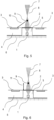
- Figs. 3 to 6 illustrate various aspects of the PM sensor of Fig. 1 .
- the light source 1 is switched on, thus emitting light towards the optical element 2.
- the optical element 2 shapes the light beam 7 and in particular focusses the light beam 7.
- PM particles 9 approach the light beam 7 as shown in Fig. 4 . This may e.g. be achieved by placing the PM sensor on a wall of a flow channel, wherein air with PM is blown through the flow channel by a fan or alternatively a heater.
- Figs. 4 to 6 depict a part of the light beam 7 with a different hatching:
- the proposed setup with a focussing optical element 2 and photodetectors 3 in the same plane has the advantage that the detection volume 8 reaches at least up to the focus of the optical element 2.
- the geometrical reasons for this have been discussed above.
- the detection volume 8 may even extend beyond the focus, i.e. a scattering particle height 11 may be larger than the focal length of the optical element 2 while the particle is still detected.
- the size and shape of the detection volume 8 may be optimized or adjusted to specific applications by varying one or more of the parameters optical power of the light source 1, focal length of the optical element 2, distance between light source 1 and optical element 2, distance between optical element 2 and photodetectors 3, sensitivity of photodetectors 3, electromagnetic shielding thus lowering the noise level, etc.
- Figs. 7 to 9 show similar embodiments of a PM sensor as Fig. 1 , however, with different optical elements 2.
- the optical element is a conventional optical lens 12, e.g. made from glass or a polymer.
- a conventional optical lens 12 needs to have a certain thickness in order to exhibit a desired focal length due to the laws of refraction.
- a diffractive optical element (DOE) 13, e.g. arranged on a membrane, may be constructed with a smaller thickness for the same focal length.
- the membrane for the DOE 13 may be exposed from the layer stack of the semiconductor chip 4 during manufacturing.
- the DOE 13 may be a metamaterial, e.g. where a surface of the membrane has been structured such that it effectively acts as an optical lens.
- Fig. 9 shows yet another optical element: A lens on a substrate, e.g. a polymer lens on a glass carrier substrate 15 as described above.
- a lens on a glass carrier substrate 15 may be manufactured as an imprint polymer lens on the glass carrier substrate 15 and then mounted on the semiconductor chip 4, e.g. by means of an adhesive. Since thermal expansion coefficients of the glass carrier substrate 15 and the semiconductor chip 4 match or are at least similar, strain in the adhesive is reduced upon temperature cycling.
- Fig. 9 further illustrates a geometrical consideration relating to the spreading of the spherical wavefront of the scattered light as explained above:
- a distance 14 of the photodetectors 3 from the optical axis, and thus from the optical element, is advantageously minimized. This leads to a large detection volume 8, or in other words, to a high PM count.
- Figs. 9 and 10 depict another advantageous feature of an embodiment of the invention.
- the side walls of the optical element 2, in this case of the substrate 15 carrying the lens, are provided with a blackening 19 or a silvering. This prevents that stray light from the optical element reaches the photodetectors 3 on a direct path, which would significantly raise the noise level and decrease the PM sensor's ability to detect PM particles, i.e. it would significantly decrease the detection volume 8.
- the blackening or silvering 19 may be achieved by applying a selective coating to the lens and the substrate 15, e.g. a chemical that binds to and blackens / silvers the glass of the substrate but not the polymer lens. In addition, such a coating is by its very nature thin and does hence not add in a material way to the lateral thickness of the optical element and hence does not worsen the shadowing described above.
- Fig. 10 shows a schematic cut through a PM sensor according to another embodiment.
- This PM sensor shares most features with the one of Fig. 1 . However, it only has photodetectors 3 on one side of the optical element, which in the shown embodiment again is a lens on a substrate 15. On the opposite side, the optical element is supported by a support 16, which may e.g. be a moulded frame or a dummy substrate spacer.
- the PM sensor of Fig. 10 may evidently have a smaller signal-to-noise ratio than the PM sensor of the previous Figs. However, the present PM sensor may be built with an even smaller form factor, making it well suited for miniaturized applications.
Landscapes
- Chemical & Material Sciences (AREA)
- Dispersion Chemistry (AREA)
- Physics & Mathematics (AREA)
- Health & Medical Sciences (AREA)
- Life Sciences & Earth Sciences (AREA)
- Analytical Chemistry (AREA)
- Biochemistry (AREA)
- General Health & Medical Sciences (AREA)
- General Physics & Mathematics (AREA)
- Immunology (AREA)
- Pathology (AREA)
- Investigating Or Analysing Materials By Optical Means (AREA)
Claims (15)
- Capteur de particules comprenant- un substrat (4),- une source de lumière (1) conçue pour émettre un faisceau de lumière (7),- un élément optique (2), et- au moins un photodétecteur (3),la source de lumière (1) étant conçue pour diriger le faisceau de lumière (7) sur l'élément optique (2),l'élément optique (2) étant conçu pour façonner le faisceau de lumière (7), formant ainsi un volume de détection (8) pour les particules (9), etl'au moins un photodétecteur (3) est conçu pour détecter de la lumière (10) diffusée par les particules (9) dans le volume de détection (8),caractérisé en ce que- le substrat est formé par une puce semi-conductrice (4),- l'au moins un photodétecteur (3) est intégré dans une surface de la puce semi-conductrice (4), la surface de la puce semi-conductrice (4) dans laquelle l'au moins un photodétecteur (3) est intégré faisant face au volume de détection (8),- le substrat forme une cavité (5),- la source de lumière (1) est disposée dans la cavité (5), et- l'élément optique (2) délimite la cavité (5) d'un côté et est adapté pour façonner le faisceau de lumière (7) afin de former le volume de détection (8) des particules (9) à l'extérieur de la cavité (5).
- Capteur de particules selon la revendication 1,dans lequel l'élément optique (2) est conçu pour focaliser le faisceau de lumière (7), en particulier, dans lequel une distance entre l'élément optique (2) et un foyer de l'élément optique est d'au moins 1 mm, et/oudans lequel la hauteur de la cavité (5) entre la source de lumière (1) et l'élément optique (2) est d'au moins 0,25 mm, en particulier d'au moins 0,45 mm.
- Capteur de particules selon l'une quelconque des revendications précédentes,la source de lumière (1) étant une diode laser ou un laser à cavité verticale émettant par la surface (VCSEL),en particulier dans lequel la longueur d'onde du faisceau de lumière (7) est comprise entre 500 nm et 1100 nm, en particulier entre 640 nm et 950 nm.
- Capteur de particules selon l'une quelconque des revendications précédentes,dans lequel l'élément optique (2) est disposé dans un plan défini par l'au moins un photodétecteur (3), oudans lequel l'élément optique (2) dépasse d'un plan défini par l'au moins photodétecteur (3) de 1 mm au maximum.
- Capteur de particules selon l'une quelconque des revendications précédentes,dans lequel l'au moins un photodétecteur (3) est disposé à une distance maximale de 2 mm de l'élément optique (2),en particulier dans lequel l'au moins un photodétecteur (3) est disposé latéralement à côté de l'élément optique (2).
- Capteur de particules selon l'une quelconque des revendications précédentes,dans lequel l'au moins un photodétecteur (3) comprend une barrette de photodétecteurs,en particulier, dans lequel la barrette de photodétecteurs (3) est répartie autour de l'élément optique (2), en particulier dans un plan commun.
- Capteur de particules selon l'une quelconque des revendications précédentes,dans lequel les photodétecteurs (3) sont séparés, sur la surface du substrat (4) faisant face au volume de détection (8), par un matériau conducteur d'électricité (19), en particulier par une métallisation du substrat,en particulier dans lequel le matériau conducteur d'électricité (19) est adapté pour protéger les photodétecteurs (3) des rayonnements électromagnétiques lorsqu'ils sont mis à la terre.
- Capteur de particules selon l'une quelconque des revendications précédentes, comprenant en outre- une unité de commande électriquement connectée à l'au moins un photodétecteur (3) et conçue pour recevoir un signal de l'au moins un photodétecteur (3) causé par de la lumière (10) diffusée par les particules (9) dans le volume de détection (8) et pour évaluer le signal en termes d'une quantité physique liée aux particules (9),l'unité de contrôle étant intégrée dans le substrat (4),en particulier, la quantité physique comprenant au moins l'un des éléments suivants : une concentration en nombre, une vitesse, une taille et une répartition de la taille des particules.
- Capteur de particules selon la revendication 8, comprenant en outre- une photodiode disposée à côté de l'élément optique (2) et conçue pour mesurer la lumière parasite provenant de l'élément optique (2),l'unité de commande étant en outre connectée à la photodiode et conçue pour déterminer une puissance optique de la source de lumière (1) à partir de la lumière parasite et pour évaluer la quantité physique liée aux particules ou commander la source de lumière (1) en fonction de la puissance optique déterminée,la photodiode étant en particulier intégrée dans le substrat (4),la photodiode étant en particulier disposée entre le substrat (4) et l'élément optique (2).
- Capteur de particules selon la revendication 8, comprenant en outre- une photodiode disposée dans ou à côté de la cavité (5) et conçue pour mesurer une émission spontanée de la source de lumière (1),l'unité de commande étant en outre connectée électriquement à la photodiode et conçue pour déterminer une puissance optique de la source de lumière (1) à partir de l'émission spontanée mesurée et pour évaluer la quantité physique liée aux particules ou commander la source de lumière (1) en fonction de la puissance optique déterminée,la photodiode étant en particulier intégrée dans le substrat (4),la source de lumière (1) comprenant en particulier un laser à cavité verticale émettant par la surface (VCSEL) et l'émission spontanée provenant d'une ou de plusieurs parois latérales du VCSEL, une ou plusieurs parois latérales étant des parois autres qu'une surface d'émission principale du VCSEL.
- Capteur de particules selon l'une quelconque des revendications précédentes,dans lequel l'élément optique (2) comprend une lentille réfractive (12) ou un élément optique diffractif (13),en particulier dans lequel l'élément optique (2) comprend une lentille en polymère imprimé (15), ouen particulier dans lequel l'élément optique (2) comprend une lentille moulée par injection,en particulier dans lequel la lentille en polymère (15) est disposée sur un substrat de verre porteur d'une épaisseur inférieure à 1000 µm, en particulier inférieure à 750 pm.
- Capteur de particules selon l'une quelconque des revendications 1 à 10,dans lequel l'élément optique (2) comprend un métamatériau transparent pour le faisceau de lumière (7), le métamatériau étant en particulier formé par une fine partie restante du substrat (4) délimitant la cavité (5),en particulier dans lequel l'épaisseur du métamatériau est inférieure à 20 µm, en particulier inférieure à 10 µm.
- Capteur de particules selon l'une quelconque des revendications précédentes, comprenant en outre- une barrière de lumière (19) entre l'élément optique (2) et l'au moins un photodétecteur (3),la barrière lumineuse (19) comprenant en particulier un noircissement ou un argentage des parois latérales de l'élément optique (2) faisant face à l'au moins un photodétecteur (3), ou une ouverture entre la source de lumière (1) et l'élément optique (2),le noircissement ou l'argenture comprenant en particulier un revêtement sélectif réagissant uniquement avec la couche de verre porteuse et non avec la lentille de polymère (15).
- Capteur de particules selon l'une quelconque des revendications précédentes,dans lequel l'au moins un photodétecteur (3) est divisé en une première partition orientée vers le volume de détection (8) et une seconde partition protégée de la lumière (10) diffusée par les particules (9) dans le volume de détection (8),l'unité de commande étant conçue pour effectuer une mesure différentielle de la première partition et de la seconde partition, en particulier en annulant les effets parasites des interférences électromagnétiques avec l'au moins un photodétecteur (3).
- Module de capteur de particules comprenant- un boîtier,- un canal d'écoulement disposé dans le boîtier,- un ventilateur ou un chauffage disposé dans le boîtier et conçu pour faire circuler l'air dans le canal d'écoulement,- le capteur de particules de l'une quelconque des revendications précédentes, disposé dans le boîtier de telle sorte qu'une partie du canal d'écoulement coïncide avec le volume de détection (8).
Priority Applications (9)
| Application Number | Priority Date | Filing Date | Title |
|---|---|---|---|
| EP20171192.6A EP3901612B1 (fr) | 2020-04-23 | 2020-04-23 | Capteur de matière particulaire intégré doté d'une cavité |
| EP20803620.2A EP4139651B1 (fr) | 2020-04-23 | 2020-11-13 | Capteur de matière particulaire intégré doté d'une cavité |
| HUE20803620A HUE072529T2 (hu) | 2020-04-23 | 2020-11-13 | Integrált részecskeérzékelõ üreggel |
| KR1020227040313A KR102864987B1 (ko) | 2020-04-23 | 2020-11-13 | 캐비티를 가지는 집적된 미립자 물질 센서 |
| PCT/EP2020/082129 WO2021213692A1 (fr) | 2020-04-23 | 2020-11-13 | Capteur de matière particulaire intégré comprenant une cavité |
| DE202020005879.3U DE202020005879U1 (de) | 2020-04-23 | 2020-11-13 | Integrierter Partikelsensor mit Hohlraum |
| CN202080100172.XA CN115516289B (zh) | 2020-04-23 | 2020-11-13 | 具有腔的集成的颗粒物质传感器 |
| JP2022563908A JP7638298B2 (ja) | 2020-04-23 | 2020-11-13 | キャビティを有する統合型粒子状物質センサー |
| US17/971,021 US11761876B2 (en) | 2020-04-23 | 2022-10-21 | Integrated particulate matter sensor with cavity |
Applications Claiming Priority (1)
| Application Number | Priority Date | Filing Date | Title |
|---|---|---|---|
| EP20171192.6A EP3901612B1 (fr) | 2020-04-23 | 2020-04-23 | Capteur de matière particulaire intégré doté d'une cavité |
Publications (2)
| Publication Number | Publication Date |
|---|---|
| EP3901612A1 EP3901612A1 (fr) | 2021-10-27 |
| EP3901612B1 true EP3901612B1 (fr) | 2024-06-12 |
Family
ID=70470799
Family Applications (2)
| Application Number | Title | Priority Date | Filing Date |
|---|---|---|---|
| EP20171192.6A Active EP3901612B1 (fr) | 2020-04-23 | 2020-04-23 | Capteur de matière particulaire intégré doté d'une cavité |
| EP20803620.2A Active EP4139651B1 (fr) | 2020-04-23 | 2020-11-13 | Capteur de matière particulaire intégré doté d'une cavité |
Family Applications After (1)
| Application Number | Title | Priority Date | Filing Date |
|---|---|---|---|
| EP20803620.2A Active EP4139651B1 (fr) | 2020-04-23 | 2020-11-13 | Capteur de matière particulaire intégré doté d'une cavité |
Country Status (8)
| Country | Link |
|---|---|
| US (1) | US11761876B2 (fr) |
| EP (2) | EP3901612B1 (fr) |
| JP (1) | JP7638298B2 (fr) |
| KR (1) | KR102864987B1 (fr) |
| CN (1) | CN115516289B (fr) |
| DE (1) | DE202020005879U1 (fr) |
| HU (1) | HUE072529T2 (fr) |
| WO (1) | WO2021213692A1 (fr) |
Families Citing this family (7)
| Publication number | Priority date | Publication date | Assignee | Title |
|---|---|---|---|---|
| KR102681896B1 (ko) * | 2022-03-21 | 2024-07-05 | (주)인프라칩 | 미세먼지농도 감지 방법 및 장치 |
| TW202407329A (zh) * | 2022-05-05 | 2024-02-16 | 香港商新發病毒診斷(香港)有限公司 | 信號檢測機構及其方法 |
| DE202022103958U1 (de) * | 2022-07-14 | 2022-07-20 | Sensirion AG | Partikelsensor |
| US12399340B2 (en) * | 2022-10-27 | 2025-08-26 | Sensirion Ag | Optical component, optoelectronic module and method of manufacture |
| EP4468370A1 (fr) | 2023-05-20 | 2024-11-27 | Sensirion AG | Puce photodectrice résistante aux interférences électromagnétiques |
| WO2025072621A1 (fr) * | 2023-09-29 | 2025-04-03 | Arizona Board Of Regents On Behalf Of The University Of Arizona | Surveillance de matière particulaire à l'aide d'un film mince spatialement incurvé |
| EP4575592A1 (fr) * | 2023-12-22 | 2025-06-25 | Sensirion AG | Composant optique et procédé de fabrication |
Family Cites Families (42)
| Publication number | Priority date | Publication date | Assignee | Title |
|---|---|---|---|---|
| US5332892A (en) * | 1991-07-25 | 1994-07-26 | Symbol Technologies, Inc. | Optical systems for bar code scanners |
| JPH05172632A (ja) * | 1991-12-26 | 1993-07-09 | Juki Corp | 光量測定装置 |
| US5963336A (en) * | 1995-10-10 | 1999-10-05 | American Air Liquide Inc. | Chamber effluent monitoring system and semiconductor processing system comprising absorption spectroscopy measurement system, and methods of use |
| WO2001064831A1 (fr) * | 2000-02-29 | 2001-09-07 | The Board Of Trustees Of The Leland Stanford Junior University | Substrat de microreseaux a photodetecteur integre et ses procedes d'utilisation |
| MXPA03007849A (es) | 2001-03-01 | 2004-10-15 | Rporation New Mexico State Uni | Dispositivos opticos y metodos que empleen nanoparticulas, microcavidades y peliculas metalicas semicontinuas. |
| GB2392308B (en) * | 2002-08-15 | 2006-10-25 | Detection Technology Oy | Packaging structure for imaging detectors |
| DE102004030418A1 (de) * | 2004-06-24 | 2006-01-19 | Robert Bosch Gmbh | Mikrostrukturierter Infrarot-Sensor und ein Verfahren zu seiner Herstellung |
| KR100684870B1 (ko) * | 2004-12-07 | 2007-02-20 | 삼성전자주식회사 | 씨모스 이미지 센서 및 그 형성 방법 |
| US7244925B2 (en) * | 2005-03-21 | 2007-07-17 | Avago Technologies Ecbu Ip (Singapore) Pte. Ltd | Compact and low profile optical navigation device |
| US8323982B2 (en) * | 2007-01-11 | 2012-12-04 | Valencell, Inc. | Photoelectrocatalytic fluid analyte sensors and methods of fabricating and using same |
| GB2448161A (en) * | 2007-04-03 | 2008-10-08 | Bookham Technology Plc | Optoelectronic device combining VCSEL and photodetector |
| KR101360294B1 (ko) * | 2008-05-21 | 2014-02-11 | 광주과학기술원 | 반사형 광학 센서장치 |
| WO2010124347A1 (fr) * | 2009-05-01 | 2010-11-04 | Xtralis Technologies Ltd | Améliorations apportées à des détecteurs de particules |
| FR2963101B1 (fr) * | 2010-07-22 | 2013-02-15 | Commissariat Energie Atomique | Detecteur de particules et procede de realisation d'un tel detecteur |
| NL2006373C2 (nl) * | 2011-03-11 | 2012-09-17 | Anteryon Internat B V | Optische eenheid. |
| KR20150062675A (ko) * | 2013-11-29 | 2015-06-08 | 서울바이오시스 주식회사 | 휴대용 공기 품질 판단 장치 |
| KR102163738B1 (ko) * | 2014-07-24 | 2020-10-08 | 삼성전자주식회사 | 미세입자 측정이 가능한 모바일 기기 및 이를 이용한 미세입자 측정 방법 |
| CA2957543A1 (fr) * | 2014-08-08 | 2016-02-11 | Quantum-Si Incorporated | Systeme optique et puce d'analyse pour sonder, detecter, et analyser des molecules |
| US10234695B2 (en) | 2015-02-16 | 2019-03-19 | Apple Inc. | Low-temperature hermetic sealing for diffractive optical element stacks |
| DE102015207289B4 (de) * | 2015-04-22 | 2025-12-24 | Robert Bosch Gmbh | Partikelsensorvorrichtung |
| WO2016175828A1 (fr) * | 2015-04-30 | 2016-11-03 | Hewlett Packard Enterprise Development Lp | Photodétecteur et récepteur intégrés de manière monolithique |
| JP6670565B2 (ja) * | 2015-07-31 | 2020-03-25 | ソニーセミコンダクタソリューションズ株式会社 | 積層レンズ構造体の製造方法及び型 |
| WO2017060164A1 (fr) * | 2015-10-08 | 2017-04-13 | Koninklijke Philips N.V. | Capteur optique pour détection de particule |
| KR102091040B1 (ko) * | 2015-11-27 | 2020-03-19 | 하이만 센서 게엠베하 | 웨이퍼-레벨 패키지의 열 적외선 센서 어레이 |
| JP6899839B2 (ja) * | 2016-03-21 | 2021-07-07 | トルンプ フォトニック コンポーネンツ ゲーエムベーハー | 超微粒子サイズ検出のためのレーザー・センサー |
| EP3225977B1 (fr) * | 2016-03-31 | 2019-03-13 | ams AG | Procédé et système de capteur pour la détection de particules |
| US10670523B2 (en) * | 2016-04-19 | 2020-06-02 | Intel Corporation | Particulate matter measurement using light sheet generation and scattering analysis |
| EP3458831B1 (fr) * | 2016-05-19 | 2024-03-06 | TRUMPF Photonic Components GmbH | Capteur optique de particules |
| WO2018047547A1 (fr) * | 2016-09-12 | 2018-03-15 | サイエンスエッジ株式会社 | Dispositif de mesure, microscope et procédé de mesure |
| CN106483051B (zh) * | 2016-09-28 | 2019-07-12 | 南京中电熊猫平板显示科技有限公司 | 一种用于移动终端测定大气颗粒物浓度的装置及移动终端 |
| US10502618B2 (en) * | 2016-12-03 | 2019-12-10 | Waymo Llc | Waveguide diffuser for light detection using an aperture |
| WO2018105975A1 (fr) | 2016-12-05 | 2018-06-14 | 엘지이노텍 주식회사 | Élément semi-conducteur, procédé de fabrication d'élément semi-conducteur et dispositif de détection |
| JP6820425B2 (ja) * | 2016-12-09 | 2021-01-27 | トルンプ フォトニック コンポーネンツ ゲゼルシャフト ミット ベシュレンクテル ハフツング | 粒子密度検出のためのレーザセンサモジュール |
| JP2018140039A (ja) | 2017-02-28 | 2018-09-13 | セイコーエプソン株式会社 | 光検出装置、粒子密度測定装置およびウエアラブル機器 |
| EP3258241B1 (fr) | 2017-09-14 | 2019-12-25 | Sensirion AG | Dispositif de capteur de particules |
| US11513050B2 (en) * | 2017-12-15 | 2022-11-29 | Ams Ag | Particulate matter sensor |
| EP3588057A1 (fr) * | 2018-06-29 | 2020-01-01 | Koninklijke Philips N.V. | Procédé de réduction de numération de particules de faux positifs d'un module de capteur de particules d'interférence |
| DE102018213932B4 (de) * | 2018-08-17 | 2024-06-20 | Robert Bosch Gmbh | Optische Partikelsensorvorrichtung und Verfahren zum Betreiben einer optischen Partikelsensorvorrichtung |
| US10788308B2 (en) * | 2018-09-21 | 2020-09-29 | Apple Inc. | Particulate matter sensors for portable electronic devices |
| US11073467B2 (en) * | 2018-09-28 | 2021-07-27 | Stmicroelectronics S.R.L. | Miniaturized optical particle detector |
| US11204513B2 (en) * | 2019-05-03 | 2021-12-21 | Yissum Research Development Company Of The Hebrew University Of Jerusamem Ltd | Integrated frequency referencing system |
| KR20230107363A (ko) * | 2020-11-24 | 2023-07-14 | 스월 비전 시스템즈 인크. | 집적된 광학 격자 커플러를 갖는 광검출기들 및 관련 방법들 |
-
2020
- 2020-04-23 EP EP20171192.6A patent/EP3901612B1/fr active Active
- 2020-11-13 EP EP20803620.2A patent/EP4139651B1/fr active Active
- 2020-11-13 CN CN202080100172.XA patent/CN115516289B/zh active Active
- 2020-11-13 DE DE202020005879.3U patent/DE202020005879U1/de active Active
- 2020-11-13 JP JP2022563908A patent/JP7638298B2/ja active Active
- 2020-11-13 HU HUE20803620A patent/HUE072529T2/hu unknown
- 2020-11-13 KR KR1020227040313A patent/KR102864987B1/ko active Active
- 2020-11-13 WO PCT/EP2020/082129 patent/WO2021213692A1/fr not_active Ceased
-
2022
- 2022-10-21 US US17/971,021 patent/US11761876B2/en active Active
Also Published As
| Publication number | Publication date |
|---|---|
| US11761876B2 (en) | 2023-09-19 |
| US20230080848A1 (en) | 2023-03-16 |
| CN115516289B (zh) | 2025-08-12 |
| JP2023522929A (ja) | 2023-06-01 |
| DE202020005879U1 (de) | 2023-02-09 |
| EP4139651B1 (fr) | 2025-05-21 |
| EP4139651A1 (fr) | 2023-03-01 |
| HUE072529T2 (hu) | 2025-11-28 |
| CN115516289A (zh) | 2022-12-23 |
| JP7638298B2 (ja) | 2025-03-03 |
| KR102864987B1 (ko) | 2025-09-26 |
| WO2021213692A1 (fr) | 2021-10-28 |
| EP3901612A1 (fr) | 2021-10-27 |
| KR20230004694A (ko) | 2023-01-06 |
Similar Documents
| Publication | Publication Date | Title |
|---|---|---|
| EP3901612B1 (fr) | Capteur de matière particulaire intégré doté d'une cavité | |
| EP3566075B1 (fr) | Capteur de proximité à divergence étroite de laser vcsel | |
| EP3896746B1 (fr) | Diode à avalanche monohotonique et procédé de fabrication, réseau de détecteurs et capteur d'image | |
| US11733355B2 (en) | Optical sensor module and method for manufacturing an optical sensor module for time-of-flight measurement | |
| CN106104296B (zh) | 包括飞行时间传感器的光学成像模块和光学检测模块 | |
| US11079321B2 (en) | NDIR detector device for detecting gases having an infrared absorption spectrum | |
| US11774282B2 (en) | Pyranometer dome soiling detection with light sensors | |
| KR102315874B1 (ko) | 미광 억제력을 갖춘 uv 광 센서, 및 uv 광을 검출하기 위한 방법 | |
| KR20190134635A (ko) | 광 검출 장치 | |
| US9103914B2 (en) | Optical angle of arrival sensors and methods for determining an angle of arrival of incident light | |
| CN113805188A (zh) | ToF型距离传感器及电子设备 | |
| US11664475B2 (en) | Electronic device comprising a carrier substrate and an encapsulating cover mounted on the carrier substrate, and corresponding mounting process | |
| US11715750B2 (en) | Optical crosstalk mitigation for a detector array in an optical receiver | |
| EP4325246A1 (fr) | Dispositif de réception et radar laser | |
| CN115704905A (zh) | 光电探测器及激光雷达 | |
| CN219758504U (zh) | 感光芯片组件、激光雷达接收器、激光雷达以及载具系统 | |
| CN115706176B (zh) | 光电探测器、设备及存储介质 | |
| JPH0666928A (ja) | 光センシング装置 | |
| WO2026087188A2 (fr) | Piège à ions et dispositif informatique quantique | |
| KR20250013177A (ko) | 미광(Stray light) 감소 시스템을 갖는 라이다(LIDAR) 유닛 |
Legal Events
| Date | Code | Title | Description |
|---|---|---|---|
| PUAI | Public reference made under article 153(3) epc to a published international application that has entered the european phase |
Free format text: ORIGINAL CODE: 0009012 |
|
| STAA | Information on the status of an ep patent application or granted ep patent |
Free format text: STATUS: THE APPLICATION HAS BEEN PUBLISHED |
|
| AK | Designated contracting states |
Kind code of ref document: A1 Designated state(s): AL AT BE BG CH CY CZ DE DK EE ES FI FR GB GR HR HU IE IS IT LI LT LU LV MC MK MT NL NO PL PT RO RS SE SI SK SM TR |
|
| B565 | Issuance of search results under rule 164(2) epc |
Effective date: 20201021 |
|
| STAA | Information on the status of an ep patent application or granted ep patent |
Free format text: STATUS: REQUEST FOR EXAMINATION WAS MADE |
|
| 17P | Request for examination filed |
Effective date: 20211214 |
|
| RBV | Designated contracting states (corrected) |
Designated state(s): AL AT BE BG CH CY CZ DE DK EE ES FI FR GB GR HR HU IE IS IT LI LT LU LV MC MK MT NL NO PL PT RO RS SE SI SK SM TR |
|
| P01 | Opt-out of the competence of the unified patent court (upc) registered |
Effective date: 20230602 |
|
| GRAP | Despatch of communication of intention to grant a patent |
Free format text: ORIGINAL CODE: EPIDOSNIGR1 |
|
| STAA | Information on the status of an ep patent application or granted ep patent |
Free format text: STATUS: GRANT OF PATENT IS INTENDED |
|
| INTG | Intention to grant announced |
Effective date: 20240201 |
|
| GRAS | Grant fee paid |
Free format text: ORIGINAL CODE: EPIDOSNIGR3 |
|
| GRAA | (expected) grant |
Free format text: ORIGINAL CODE: 0009210 |
|
| STAA | Information on the status of an ep patent application or granted ep patent |
Free format text: STATUS: THE PATENT HAS BEEN GRANTED |
|
| AK | Designated contracting states |
Kind code of ref document: B1 Designated state(s): AL AT BE BG CH CY CZ DE DK EE ES FI FR GB GR HR HU IE IS IT LI LT LU LV MC MK MT NL NO PL PT RO RS SE SI SK SM TR |
|
| REG | Reference to a national code |
Ref country code: GB Ref legal event code: FG4D |
|
| REG | Reference to a national code |
Ref country code: CH Ref legal event code: EP |
|
| REG | Reference to a national code |
Ref country code: DE Ref legal event code: R096 Ref document number: 602020032189 Country of ref document: DE |
|
| REG | Reference to a national code |
Ref country code: IE Ref legal event code: FG4D |
|
| PG25 | Lapsed in a contracting state [announced via postgrant information from national office to epo] |
Ref country code: BG Free format text: LAPSE BECAUSE OF FAILURE TO SUBMIT A TRANSLATION OF THE DESCRIPTION OR TO PAY THE FEE WITHIN THE PRESCRIBED TIME-LIMIT Effective date: 20240612 |
|
| PG25 | Lapsed in a contracting state [announced via postgrant information from national office to epo] |
Ref country code: FI Free format text: LAPSE BECAUSE OF FAILURE TO SUBMIT A TRANSLATION OF THE DESCRIPTION OR TO PAY THE FEE WITHIN THE PRESCRIBED TIME-LIMIT Effective date: 20240612 Ref country code: HR Free format text: LAPSE BECAUSE OF FAILURE TO SUBMIT A TRANSLATION OF THE DESCRIPTION OR TO PAY THE FEE WITHIN THE PRESCRIBED TIME-LIMIT Effective date: 20240612 |
|
| REG | Reference to a national code |
Ref country code: LT Ref legal event code: MG9D |
|
| PG25 | Lapsed in a contracting state [announced via postgrant information from national office to epo] |
Ref country code: GR Free format text: LAPSE BECAUSE OF FAILURE TO SUBMIT A TRANSLATION OF THE DESCRIPTION OR TO PAY THE FEE WITHIN THE PRESCRIBED TIME-LIMIT Effective date: 20240913 |
|
| REG | Reference to a national code |
Ref country code: NL Ref legal event code: MP Effective date: 20240612 |
|
| PG25 | Lapsed in a contracting state [announced via postgrant information from national office to epo] |
Ref country code: ES Free format text: LAPSE BECAUSE OF FAILURE TO SUBMIT A TRANSLATION OF THE DESCRIPTION OR TO PAY THE FEE WITHIN THE PRESCRIBED TIME-LIMIT Effective date: 20240612 |
|
| PG25 | Lapsed in a contracting state [announced via postgrant information from national office to epo] |
Ref country code: LV Free format text: LAPSE BECAUSE OF FAILURE TO SUBMIT A TRANSLATION OF THE DESCRIPTION OR TO PAY THE FEE WITHIN THE PRESCRIBED TIME-LIMIT Effective date: 20240612 |
|
| PG25 | Lapsed in a contracting state [announced via postgrant information from national office to epo] |
Ref country code: NO Free format text: LAPSE BECAUSE OF FAILURE TO SUBMIT A TRANSLATION OF THE DESCRIPTION OR TO PAY THE FEE WITHIN THE PRESCRIBED TIME-LIMIT Effective date: 20240912 Ref country code: LV Free format text: LAPSE BECAUSE OF FAILURE TO SUBMIT A TRANSLATION OF THE DESCRIPTION OR TO PAY THE FEE WITHIN THE PRESCRIBED TIME-LIMIT Effective date: 20240612 Ref country code: HR Free format text: LAPSE BECAUSE OF FAILURE TO SUBMIT A TRANSLATION OF THE DESCRIPTION OR TO PAY THE FEE WITHIN THE PRESCRIBED TIME-LIMIT Effective date: 20240612 Ref country code: GR Free format text: LAPSE BECAUSE OF FAILURE TO SUBMIT A TRANSLATION OF THE DESCRIPTION OR TO PAY THE FEE WITHIN THE PRESCRIBED TIME-LIMIT Effective date: 20240913 Ref country code: FI Free format text: LAPSE BECAUSE OF FAILURE TO SUBMIT A TRANSLATION OF THE DESCRIPTION OR TO PAY THE FEE WITHIN THE PRESCRIBED TIME-LIMIT Effective date: 20240612 Ref country code: ES Free format text: LAPSE BECAUSE OF FAILURE TO SUBMIT A TRANSLATION OF THE DESCRIPTION OR TO PAY THE FEE WITHIN THE PRESCRIBED TIME-LIMIT Effective date: 20240612 Ref country code: BG Free format text: LAPSE BECAUSE OF FAILURE TO SUBMIT A TRANSLATION OF THE DESCRIPTION OR TO PAY THE FEE WITHIN THE PRESCRIBED TIME-LIMIT Effective date: 20240612 Ref country code: RS Free format text: LAPSE BECAUSE OF FAILURE TO SUBMIT A TRANSLATION OF THE DESCRIPTION OR TO PAY THE FEE WITHIN THE PRESCRIBED TIME-LIMIT Effective date: 20240912 |
|
| PG25 | Lapsed in a contracting state [announced via postgrant information from national office to epo] |
Ref country code: NL Free format text: LAPSE BECAUSE OF FAILURE TO SUBMIT A TRANSLATION OF THE DESCRIPTION OR TO PAY THE FEE WITHIN THE PRESCRIBED TIME-LIMIT Effective date: 20240612 |
|
| REG | Reference to a national code |
Ref country code: AT Ref legal event code: MK05 Ref document number: 1694665 Country of ref document: AT Kind code of ref document: T Effective date: 20240612 |
|
| PG25 | Lapsed in a contracting state [announced via postgrant information from national office to epo] |
Ref country code: NL Free format text: LAPSE BECAUSE OF FAILURE TO SUBMIT A TRANSLATION OF THE DESCRIPTION OR TO PAY THE FEE WITHIN THE PRESCRIBED TIME-LIMIT Effective date: 20240612 |
|
| PG25 | Lapsed in a contracting state [announced via postgrant information from national office to epo] |
Ref country code: PT Free format text: LAPSE BECAUSE OF FAILURE TO SUBMIT A TRANSLATION OF THE DESCRIPTION OR TO PAY THE FEE WITHIN THE PRESCRIBED TIME-LIMIT Effective date: 20241014 |
|
| PG25 | Lapsed in a contracting state [announced via postgrant information from national office to epo] |
Ref country code: PT Free format text: LAPSE BECAUSE OF FAILURE TO SUBMIT A TRANSLATION OF THE DESCRIPTION OR TO PAY THE FEE WITHIN THE PRESCRIBED TIME-LIMIT Effective date: 20241014 |
|
| PG25 | Lapsed in a contracting state [announced via postgrant information from national office to epo] |
Ref country code: PL Free format text: LAPSE BECAUSE OF FAILURE TO SUBMIT A TRANSLATION OF THE DESCRIPTION OR TO PAY THE FEE WITHIN THE PRESCRIBED TIME-LIMIT Effective date: 20240612 |
|
| PG25 | Lapsed in a contracting state [announced via postgrant information from national office to epo] |
Ref country code: EE Free format text: LAPSE BECAUSE OF FAILURE TO SUBMIT A TRANSLATION OF THE DESCRIPTION OR TO PAY THE FEE WITHIN THE PRESCRIBED TIME-LIMIT Effective date: 20240612 |
|
| PG25 | Lapsed in a contracting state [announced via postgrant information from national office to epo] |
Ref country code: AT Free format text: LAPSE BECAUSE OF FAILURE TO SUBMIT A TRANSLATION OF THE DESCRIPTION OR TO PAY THE FEE WITHIN THE PRESCRIBED TIME-LIMIT Effective date: 20240612 Ref country code: IS Free format text: LAPSE BECAUSE OF FAILURE TO SUBMIT A TRANSLATION OF THE DESCRIPTION OR TO PAY THE FEE WITHIN THE PRESCRIBED TIME-LIMIT Effective date: 20241012 |
|
| PG25 | Lapsed in a contracting state [announced via postgrant information from national office to epo] |
Ref country code: CZ Free format text: LAPSE BECAUSE OF FAILURE TO SUBMIT A TRANSLATION OF THE DESCRIPTION OR TO PAY THE FEE WITHIN THE PRESCRIBED TIME-LIMIT Effective date: 20240612 |
|
| PG25 | Lapsed in a contracting state [announced via postgrant information from national office to epo] |
Ref country code: SK Free format text: LAPSE BECAUSE OF FAILURE TO SUBMIT A TRANSLATION OF THE DESCRIPTION OR TO PAY THE FEE WITHIN THE PRESCRIBED TIME-LIMIT Effective date: 20240612 Ref country code: RO Free format text: LAPSE BECAUSE OF FAILURE TO SUBMIT A TRANSLATION OF THE DESCRIPTION OR TO PAY THE FEE WITHIN THE PRESCRIBED TIME-LIMIT Effective date: 20240612 |
|
| PG25 | Lapsed in a contracting state [announced via postgrant information from national office to epo] |
Ref country code: SM Free format text: LAPSE BECAUSE OF FAILURE TO SUBMIT A TRANSLATION OF THE DESCRIPTION OR TO PAY THE FEE WITHIN THE PRESCRIBED TIME-LIMIT Effective date: 20240612 |
|
| PG25 | Lapsed in a contracting state [announced via postgrant information from national office to epo] |
Ref country code: SM Free format text: LAPSE BECAUSE OF FAILURE TO SUBMIT A TRANSLATION OF THE DESCRIPTION OR TO PAY THE FEE WITHIN THE PRESCRIBED TIME-LIMIT Effective date: 20240612 Ref country code: SK Free format text: LAPSE BECAUSE OF FAILURE TO SUBMIT A TRANSLATION OF THE DESCRIPTION OR TO PAY THE FEE WITHIN THE PRESCRIBED TIME-LIMIT Effective date: 20240612 Ref country code: RO Free format text: LAPSE BECAUSE OF FAILURE TO SUBMIT A TRANSLATION OF THE DESCRIPTION OR TO PAY THE FEE WITHIN THE PRESCRIBED TIME-LIMIT Effective date: 20240612 Ref country code: PL Free format text: LAPSE BECAUSE OF FAILURE TO SUBMIT A TRANSLATION OF THE DESCRIPTION OR TO PAY THE FEE WITHIN THE PRESCRIBED TIME-LIMIT Effective date: 20240612 Ref country code: IS Free format text: LAPSE BECAUSE OF FAILURE TO SUBMIT A TRANSLATION OF THE DESCRIPTION OR TO PAY THE FEE WITHIN THE PRESCRIBED TIME-LIMIT Effective date: 20241012 Ref country code: EE Free format text: LAPSE BECAUSE OF FAILURE TO SUBMIT A TRANSLATION OF THE DESCRIPTION OR TO PAY THE FEE WITHIN THE PRESCRIBED TIME-LIMIT Effective date: 20240612 Ref country code: CZ Free format text: LAPSE BECAUSE OF FAILURE TO SUBMIT A TRANSLATION OF THE DESCRIPTION OR TO PAY THE FEE WITHIN THE PRESCRIBED TIME-LIMIT Effective date: 20240612 Ref country code: AT Free format text: LAPSE BECAUSE OF FAILURE TO SUBMIT A TRANSLATION OF THE DESCRIPTION OR TO PAY THE FEE WITHIN THE PRESCRIBED TIME-LIMIT Effective date: 20240612 |
|
| PG25 | Lapsed in a contracting state [announced via postgrant information from national office to epo] |
Ref country code: IT Free format text: LAPSE BECAUSE OF FAILURE TO SUBMIT A TRANSLATION OF THE DESCRIPTION OR TO PAY THE FEE WITHIN THE PRESCRIBED TIME-LIMIT Effective date: 20240612 |
|
| REG | Reference to a national code |
Ref country code: DE Ref legal event code: R097 Ref document number: 602020032189 Country of ref document: DE |
|
| PG25 | Lapsed in a contracting state [announced via postgrant information from national office to epo] |
Ref country code: DK Free format text: LAPSE BECAUSE OF FAILURE TO SUBMIT A TRANSLATION OF THE DESCRIPTION OR TO PAY THE FEE WITHIN THE PRESCRIBED TIME-LIMIT Effective date: 20240612 |
|
| PLBE | No opposition filed within time limit |
Free format text: ORIGINAL CODE: 0009261 |
|
| STAA | Information on the status of an ep patent application or granted ep patent |
Free format text: STATUS: NO OPPOSITION FILED WITHIN TIME LIMIT |
|
| 26N | No opposition filed |
Effective date: 20250313 |
|
| PGFP | Annual fee paid to national office [announced via postgrant information from national office to epo] |
Ref country code: DE Payment date: 20250417 Year of fee payment: 6 |
|
| PGFP | Annual fee paid to national office [announced via postgrant information from national office to epo] |
Ref country code: FR Payment date: 20250422 Year of fee payment: 6 |
|
| PGFP | Annual fee paid to national office [announced via postgrant information from national office to epo] |
Ref country code: CH Payment date: 20250501 Year of fee payment: 6 |
|
| PG25 | Lapsed in a contracting state [announced via postgrant information from national office to epo] |
Ref country code: SE Free format text: LAPSE BECAUSE OF FAILURE TO SUBMIT A TRANSLATION OF THE DESCRIPTION OR TO PAY THE FEE WITHIN THE PRESCRIBED TIME-LIMIT Effective date: 20240612 |
|
| PG25 | Lapsed in a contracting state [announced via postgrant information from national office to epo] |
Ref country code: LU Free format text: LAPSE BECAUSE OF NON-PAYMENT OF DUE FEES Effective date: 20250423 |
|
| PG25 | Lapsed in a contracting state [announced via postgrant information from national office to epo] |
Ref country code: MC Free format text: LAPSE BECAUSE OF FAILURE TO SUBMIT A TRANSLATION OF THE DESCRIPTION OR TO PAY THE FEE WITHIN THE PRESCRIBED TIME-LIMIT Effective date: 20240612 |
|
| REG | Reference to a national code |
Ref country code: BE Ref legal event code: MM Effective date: 20250430 |
|
| PG25 | Lapsed in a contracting state [announced via postgrant information from national office to epo] |
Ref country code: BE Free format text: LAPSE BECAUSE OF NON-PAYMENT OF DUE FEES Effective date: 20250430 |
|
| PGFP | Annual fee paid to national office [announced via postgrant information from national office to epo] |
Ref country code: GB Payment date: 20260324 Year of fee payment: 7 |
|
| PG25 | Lapsed in a contracting state [announced via postgrant information from national office to epo] |
Ref country code: IE Free format text: LAPSE BECAUSE OF NON-PAYMENT OF DUE FEES Effective date: 20250423 |