EP3901992B1 - Erweiterte ätztechniken für geradlinige, grosse und gleichmässige rippen über mehrere rippenneigungsstrukturen - Google Patents
Erweiterte ätztechniken für geradlinige, grosse und gleichmässige rippen über mehrere rippenneigungsstrukturen Download PDFInfo
- Publication number
- EP3901992B1 EP3901992B1 EP21178944.1A EP21178944A EP3901992B1 EP 3901992 B1 EP3901992 B1 EP 3901992B1 EP 21178944 A EP21178944 A EP 21178944A EP 3901992 B1 EP3901992 B1 EP 3901992B1
- Authority
- EP
- European Patent Office
- Prior art keywords
- fins
- hard mask
- substrate
- nested
- etching process
- Prior art date
- Legal status (The legal status is an assumption and is not a legal conclusion. Google has not performed a legal analysis and makes no representation as to the accuracy of the status listed.)
- Active
Links
Images


Classifications
-
- H—ELECTRICITY
- H10—SEMICONDUCTOR DEVICES; ELECTRIC SOLID-STATE DEVICES NOT OTHERWISE PROVIDED FOR
- H10P—GENERIC PROCESSES OR APPARATUS FOR THE MANUFACTURE OR TREATMENT OF DEVICES COVERED BY CLASS H10
- H10P50/00—Etching of wafers, substrates or parts of devices
- H10P50/20—Dry etching; Plasma etching; Reactive-ion etching
- H10P50/24—Dry etching; Plasma etching; Reactive-ion etching of semiconductor materials
- H10P50/242—Dry etching; Plasma etching; Reactive-ion etching of semiconductor materials of Group IV materials
-
- H—ELECTRICITY
- H05—ELECTRIC TECHNIQUES NOT OTHERWISE PROVIDED FOR
- H05H—PLASMA TECHNIQUE; PRODUCTION OF ACCELERATED ELECTRICALLY-CHARGED PARTICLES OR OF NEUTRONS; PRODUCTION OR ACCELERATION OF NEUTRAL MOLECULAR OR ATOMIC BEAMS
- H05H1/00—Generating plasma; Handling plasma
- H05H1/24—Generating plasma
- H05H1/46—Generating plasma using applied electromagnetic fields, e.g. high frequency or microwave energy
-
- H—ELECTRICITY
- H10—SEMICONDUCTOR DEVICES; ELECTRIC SOLID-STATE DEVICES NOT OTHERWISE PROVIDED FOR
- H10D—INORGANIC ELECTRIC SEMICONDUCTOR DEVICES
- H10D30/00—Field-effect transistors [FET]
- H10D30/01—Manufacture or treatment
- H10D30/021—Manufacture or treatment of FETs having insulated gates [IGFET]
- H10D30/024—Manufacture or treatment of FETs having insulated gates [IGFET] of fin field-effect transistors [FinFET]
-
- H—ELECTRICITY
- H10—SEMICONDUCTOR DEVICES; ELECTRIC SOLID-STATE DEVICES NOT OTHERWISE PROVIDED FOR
- H10D—INORGANIC ELECTRIC SEMICONDUCTOR DEVICES
- H10D62/00—Semiconductor bodies, or regions thereof, of devices having potential barriers
- H10D62/10—Shapes, relative sizes or dispositions of the regions of the semiconductor bodies; Shapes of the semiconductor bodies
- H10D62/113—Isolations within a component, i.e. internal isolations
-
- H—ELECTRICITY
- H10—SEMICONDUCTOR DEVICES; ELECTRIC SOLID-STATE DEVICES NOT OTHERWISE PROVIDED FOR
- H10D—INORGANIC ELECTRIC SEMICONDUCTOR DEVICES
- H10D62/00—Semiconductor bodies, or regions thereof, of devices having potential barriers
- H10D62/10—Shapes, relative sizes or dispositions of the regions of the semiconductor bodies; Shapes of the semiconductor bodies
- H10D62/117—Shapes of semiconductor bodies
-
- H—ELECTRICITY
- H10—SEMICONDUCTOR DEVICES; ELECTRIC SOLID-STATE DEVICES NOT OTHERWISE PROVIDED FOR
- H10P—GENERIC PROCESSES OR APPARATUS FOR THE MANUFACTURE OR TREATMENT OF DEVICES COVERED BY CLASS H10
- H10P14/00—Formation of materials, e.g. in the shape of layers or pillars
- H10P14/60—Formation of materials, e.g. in the shape of layers or pillars of insulating materials
- H10P14/65—Formation of materials, e.g. in the shape of layers or pillars of insulating materials characterised by treatments performed before or after the formation of the materials
- H10P14/6502—Formation of materials, e.g. in the shape of layers or pillars of insulating materials characterised by treatments performed before or after the formation of the materials of treatments performed before formation of the materials
- H10P14/6512—Formation of materials, e.g. in the shape of layers or pillars of insulating materials characterised by treatments performed before or after the formation of the materials of treatments performed before formation of the materials by exposure to a gas or vapour
- H10P14/6514—Formation of materials, e.g. in the shape of layers or pillars of insulating materials characterised by treatments performed before or after the formation of the materials of treatments performed before formation of the materials by exposure to a gas or vapour by exposure to a plasma
-
- H—ELECTRICITY
- H10—SEMICONDUCTOR DEVICES; ELECTRIC SOLID-STATE DEVICES NOT OTHERWISE PROVIDED FOR
- H10P—GENERIC PROCESSES OR APPARATUS FOR THE MANUFACTURE OR TREATMENT OF DEVICES COVERED BY CLASS H10
- H10P50/00—Etching of wafers, substrates or parts of devices
- H10P50/20—Dry etching; Plasma etching; Reactive-ion etching
- H10P50/26—Dry etching; Plasma etching; Reactive-ion etching of conductive or resistive materials
- H10P50/264—Dry etching; Plasma etching; Reactive-ion etching of conductive or resistive materials by chemical means
- H10P50/266—Dry etching; Plasma etching; Reactive-ion etching of conductive or resistive materials by chemical means by vapour etching only
- H10P50/267—Dry etching; Plasma etching; Reactive-ion etching of conductive or resistive materials by chemical means by vapour etching only using plasmas
-
- H—ELECTRICITY
- H10—SEMICONDUCTOR DEVICES; ELECTRIC SOLID-STATE DEVICES NOT OTHERWISE PROVIDED FOR
- H10P—GENERIC PROCESSES OR APPARATUS FOR THE MANUFACTURE OR TREATMENT OF DEVICES COVERED BY CLASS H10
- H10P50/00—Etching of wafers, substrates or parts of devices
- H10P50/20—Dry etching; Plasma etching; Reactive-ion etching
- H10P50/28—Dry etching; Plasma etching; Reactive-ion etching of insulating materials
- H10P50/282—Dry etching; Plasma etching; Reactive-ion etching of insulating materials of inorganic materials
- H10P50/283—Dry etching; Plasma etching; Reactive-ion etching of insulating materials of inorganic materials by chemical means
-
- H—ELECTRICITY
- H10—SEMICONDUCTOR DEVICES; ELECTRIC SOLID-STATE DEVICES NOT OTHERWISE PROVIDED FOR
- H10P—GENERIC PROCESSES OR APPARATUS FOR THE MANUFACTURE OR TREATMENT OF DEVICES COVERED BY CLASS H10
- H10P50/00—Etching of wafers, substrates or parts of devices
- H10P50/69—Etching of wafers, substrates or parts of devices using masks for semiconductor materials
- H10P50/691—Etching of wafers, substrates or parts of devices using masks for semiconductor materials for Group V materials or Group III-V materials
- H10P50/693—Etching of wafers, substrates or parts of devices using masks for semiconductor materials for Group V materials or Group III-V materials characterised by their size, orientation, disposition, behaviour or shape, in horizontal or vertical plane
- H10P50/694—Etching of wafers, substrates or parts of devices using masks for semiconductor materials for Group V materials or Group III-V materials characterised by their size, orientation, disposition, behaviour or shape, in horizontal or vertical plane characterised by their behaviour during the process, e.g. soluble masks or redeposited masks
-
- H—ELECTRICITY
- H10—SEMICONDUCTOR DEVICES; ELECTRIC SOLID-STATE DEVICES NOT OTHERWISE PROVIDED FOR
- H10P—GENERIC PROCESSES OR APPARATUS FOR THE MANUFACTURE OR TREATMENT OF DEVICES COVERED BY CLASS H10
- H10P50/00—Etching of wafers, substrates or parts of devices
- H10P50/69—Etching of wafers, substrates or parts of devices using masks for semiconductor materials
- H10P50/691—Etching of wafers, substrates or parts of devices using masks for semiconductor materials for Group V materials or Group III-V materials
- H10P50/693—Etching of wafers, substrates or parts of devices using masks for semiconductor materials for Group V materials or Group III-V materials characterised by their size, orientation, disposition, behaviour or shape, in horizontal or vertical plane
- H10P50/695—Etching of wafers, substrates or parts of devices using masks for semiconductor materials for Group V materials or Group III-V materials characterised by their size, orientation, disposition, behaviour or shape, in horizontal or vertical plane characterised by the process involved to create the mask, e.g. lift-off masks or sidewalls or to modify the mask
-
- H—ELECTRICITY
- H10—SEMICONDUCTOR DEVICES; ELECTRIC SOLID-STATE DEVICES NOT OTHERWISE PROVIDED FOR
- H10P—GENERIC PROCESSES OR APPARATUS FOR THE MANUFACTURE OR TREATMENT OF DEVICES COVERED BY CLASS H10
- H10P95/00—Generic processes or apparatus for manufacture or treatments not covered by the other groups of this subclass
- H10P95/90—Thermal treatments, e.g. annealing or sintering
Definitions
- non-planar fin based transistor devices have enabled increased performance with a smaller device footprint. Fins that are substantially rectangular in shape have improved short channel effects compared to fins with trapezoidal or triangular shapes. This leads to higher performance for a given voltage overdrive. Rectangular fins also enable consistent device performance across the fin height with no degradation in current.
- micro loading effects occur when the CD and pitch of the fins is small enough to create different active ion accessibility at the surface of the substrate during an etching process. This results in a structurally dependent etch bias due to localized enhanced etching or plasma deposition. Additionally, the micro loading effect becomes a more significant problem when the pitch between fin based structures is non-uniform.
- nested fins and isolated fins are formed with a single etching process
- the widths of the nested fins will not be equal to the widths of the isolated fins, because the micro loading effect will be different for each type of fin. Accordingly, it becomes increasingly difficult to design circuitry that includes fin based transistor devices that require non-uniform spacing.
- nested fins will have different metrics, such as leakage current and threshold voltage, than isolated fins, even though both fins are designed to perform equivalently.
- WO 2008/103454 A2 discloses a semicondctor device comprising a monocrystalline silicon substrate including a first group of densely spaced fins and a second group of isolated fins. The spacing between the fins of second group is larger spacing than the spacing between the fins of the first group.
- Embodiments of the invention prevent micro loading effects from causing a significant difference in the widths of isolated fins and nested fins.
- Embodiments of the invention utilize multiple substrate etching processes to produce uniform fin widths with rectangular cross sections in both nested and isolated fin structures formed on the same substrate. Uniform fin width allows for the use of multi-fin devices that have uniform metrics, such as threshold voltage and leakage current, in the nested and isolated fin structures. Furthermore, uniform width in isolated and nested fins allows for the use of isolated fins in circuitry, such as an IC device.
- a hard mask patterning process may be included that transfers the fin shapes formed in a dummy hard mask into a hard mask layer.
- the hard mask etching process utilizes an etching chemistry with a high ratio of hydrogen to oxygen.
- the increased hydrogen concentration is obtained by utilizing an etching chemistry comprising CH 3 F.
- a breakthrough etch may be utilized to remove portions of an etchstop layer above the substrate in which the fins will be formed.
- a first substrate etching process etches the substrate to a first depth.
- Embodiments of the invention include fin based devices with a first depth between 70 nm and 100 nm.
- Embodiments of the first etching process utilize a chemistry that passivates the sidewalls to preserve the fin width.
- the first etching process may utilize a chemistry comprising HBr, O 2 and CF 4 .
- the first substrate etching process may have a lateral passivation rate that is greater for isolated fins than the lateral passivating rate for nested fins.
- a first substrate etching process may result in the nested fins having a smaller width 'than the width of the isolated fins.
- embodiments of the invention may utilise a second etching process may be included to equalize the widths of the isolated fins and the nested fins.
- the second etching process may equalize the widths of the fins by utilizing an etching chemistry that has a lateral etch rate that is greater for isolated fins than the lateral etch rate for nested fins.
- Embodiments of the invention utilize a chemistry comprising Cl 2 , Ar, and CH 4 for the second substrate etching process.
- the substrate is etched to a second depth.
- Embodiments of the invention may include a second depth that is between 130 nm and 170 nm.
- Figure 1 is a flow diagram that illustrates a method 140 of forming high aspect ratio fins with uniform widths.
- the remaining spacers may be used as the isolated features 105 and the nested features 106 that form the dummy hard mask 104.
- the double patterning process may be repeated one or more times, with the final remaining set of spacers being utilized as the isolated and nested features 105, 106 of the dummy hard mask 104.
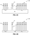
- the dummy hard mask 104 is formed from a material that is resistant to an etching process that will selectively etch through the hard mask layer 103 that is disposed below it, as shown in Figure 2A .
- the dummy hard mask 104 may be an oxide material, such as silicon dioxide.
- the hard mask layer 103 is a material that is resistant to an etchant that will selectively etch the substrate 101.
- the hard mask layer 103 is a nitride.
- a hard mask layer 103 is a thermally grown nitride, such as S1 3 N 4 .
- a hard mask layer 103 has a thickness between 40 nm and 60 nm. It is possible to include forming the hard mask layer 103 with processes such as, chemical vapor deposition, CVD, physical vapor deposition, PVD, or atomic layer deposition , ALD.
- etch stop layer 102 may be included.
- the etch stop layer 102 is disposed on a top surface of the semiconductor substrate 101, as shown in Figure 2A .
- a hard mask etching process is implemented to etch through the hard mask layer 103.
- the hard mask etching process utilizes the dummy hard mask 104 as a mask in order to transfer the isolated and nested features 105, 106 into the hard mask layer 103 to form isolated hard mask features 107 and nested hard mask features 108.
- the isolated hard mask features 107 and the nested hard mask features 108 are aligned with the isolated and nested dummy hard mask features 105 and 106, respectively.
- Figure 2B is an illustration of the hard mask layer 103 after it has been patterned with a hard mask etching process in order to form the isolated hard mask features 107 and the nested hard mask features 108.
- plasma density refers to the density of the ions and radicals present in the plasma.
- a high density plasma would have a greater concentration of ions and radicals per unit area than a low density plasma.
- the plasma density may be varied above different portions of the substrate.
- the plasma density may be varied by altering the magnetic field of the plasma processing chamber.
- the plasma density above the center of the substrate may be higher than a plasma density above the edge of the substrate. According to an embodiment of the invention the plasma density may be approximately 5% to 8% higher above the center of the substrate.
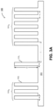
- Isolated fins and nested fins are alike, with the exception of their spacing from adjacent fins 111.
- the uniform shape and width of the isolated and the nested fins 111 1 , 11I N allows for the use of multi-fin devices that have uniform metrics, such as threshold voltage and leakage current. As such, uniform width in nested and isolated fins allows for the use of isolated fins in circuitry, such as an IC device
- the transistor devices may include fin-FET devices, such as a tri-gate device, formed on the fins 111.
- a shallow trench isolation (STI) layer 130 is disposed above the substrate 101 and between the fins 111.
- the STI layer 130 may be a silicon dioxide, or the like, as is known in the art.
- a gate dielectric 131 may be disposed over the portions of the fins 111 that extend above the STI layer 130.
- a gate metal 132 may be disposed over each fin 111. As shown in in Figure 3B , It is possible to include a single block of gate metal 132 disposed over the nested fins.
- the transistor device formed on the isolated fin 11 li can be controlled independent of the nested fins.
- source/drain (S/D) regions may be formed in the fins 111 on opposing sides of the gate metal (i.e., into the plane of the page and out of the plane of the page).
- the fins may be suitably doped with n-type and/or p-type dopants in order to form n-MOS and/or P-MOS devices
- high aspect ratio fins described are not limited to use with electrical devices and may also be utilized in nanostructures such as those used in nanoelectromechanical systems (NEMS).
- NEMS nanoelectromechanical systems
- Figure 4 illustrates a computing device 400 in accordance with one implementation.
- the computing device 400 houses a board 402.
- the board 402 may include a number of components, including but not limited to a processor 404 and at least one communication chip 406.
- the processor 404 is physically and electrically coupled to the board 402.
- the at least one communication chip 406 is also physically and electrically coupled to the board 402.
- the communication chip 406 is part of the processor 404.
- computing device 400 may include other components that may or may not be physically and electrically coupled to the board 402. These other components include, but are not limited to, volatile memory (e.g., DRAM), non-volatile memory (e.g., ROM), flash memory, a graphics processor, a digital signal processor, a crypto processor, a chipset, an antenna, a display, a touchscreen display, a touchscreen controller, a battery, an audio codec, a video codec, a power amplifier, a global positioning system (GPS) device, a compass, an accelerometer, a gyroscope, a speaker, a camera, and a mass storage device (such as hard disk drive, compact disk (CD), digital versatile disk (DVD), and so forth).
- volatile memory e.g., DRAM
- non-volatile memory e.g., ROM
- flash memory e.g., a graphics processor, a digital signal processor, a crypto processor, a chipset, an antenna, a
- the communication chip 406 enables wireless communications for the transfer of data to and from the computing device 400.
- wireless and its derivatives may be used to describe circuits, devices, systems, methods, techniques, communications channels, etc., that may communicate data through the use of modulated electromagnetic radiation through a non-solid medium. The term does not imply that the associated devices do not contain any wires, although in some embodiments they might not.
- the communication chip 406 may implement any of a number of wireless standards or protocols, including but not limited to Wi-Fi (IEEE 802.11 family), WiMAX (IEEE 802.16 family), IEEE 802.20, long term evolution (LTE), Ev-DO, HSPA+, HSDPA+, HSUPA+, EDGE, GSM, GPRS, CDMA, TDMA, DECT, Bluetooth, derivatives thereof, as well as any other wireless protocols that are designated as 3G, 4G, 5G, and beyond.
- the computing device 400 may include a plurality of communication chips 406.
- a first communication chip 406 may be dedicated to shorter range wireless communications such as Wi-Fi and Bluetooth and a second communication chip 406 may be dedicated to longer range wireless communications such as GPS, EDGE, GPRS, CDMA, WiMAX, LTE, Ev-DO, and others.
- the processor 404 of the computing device 400 includes an integrated circuit die packaged within the processor 404.
- the integrated circuit die of the processor includes one or more devices, such as MOS-FET transistors formed on high aspect ratio fins formed in accordance with implementations of the invention.
- the term "processor" may refer to any device or portion of a device that processes electronic data from registers and/or memory to transform that electronic data into other electronic data that may be stored in registers and/or memory.
- the communication chip 406 also includes an integrated circuit die packaged within the communication chip 406.
- the integrated circuit die of the communication chip includes one or more devices, such as MOS-FET transistors formed on high aspect ratio fins formed in accordance with implementations of the invention.
- the computing device 400 may be a laptop, a netbook, a notebook, an ultrabook, a smartphone, a tablet, a personal digital assistant (PDA), an ultra mobile PC, a mobile phone, a desktop computer, a server, a printer, a scanner, a monitor, a set-top box, an entertainment control unit, a digital camera, a portable music player, or a digital video recorder.
- PDA personal digital assistant
- the computing device 400 may be any other electronic device that processes data.
Landscapes
- Physics & Mathematics (AREA)
- Engineering & Computer Science (AREA)
- Plasma & Fusion (AREA)
- Electromagnetism (AREA)
- Spectroscopy & Molecular Physics (AREA)
- Drying Of Semiconductors (AREA)
Claims (12)
- Halbleiterstruktur, die durch das Verfahren nach Anspruch 3 erhalten wird, umfassend:ein monokristallines Siliciumsubstrat (101);eine verschachtelte Gruppierung von monokristallinen Siliciumrippen (111N) und eine monokristalline isolierte Siliciumrippe (111I), wobei sich die verschachtelte Gruppierung von Rippen und die isolierte Rippe von dem monokristallinen Siliciumsubstrat erstrecken, und wobei eine flache Grabenisolierschicht (130) auf dem Substrat und zwischen all den Rippen abgeschieden ist; wobei die verschachtelte Gruppierung von monokristallinen Siliciumrippen Folgendes umfasst:eine erste monokristalline Siliciumrippe mit einer Oberseite und sich lateral gegenüberliegenden Seitenwänden und mit einer Form, einer Breite, einer Höhe und einem Aspektverhältnis von Höhe zu Breite, wobei die Breite kleiner als 15 Nanometer ist, die Höhe größer als 100 Nanometer ist, und wobei das Aspektverhältnis von Höhe zu Breite größer 10:1 ist;eine zweite monokristalline Siliciumrippe mit einer Oberseite und sich lateral gegenüberliegenden Seitenwänden und mit der Form, der Breite, der Höhe und dem Aspektverhältnis von Höhe zu Breite; undeine dritte monokristalline Siliciumrippe mit einer Oberseite und sich lateral gegenüberliegenden Seitenwänden und mit der Form, der Breite, der Höhe und dem Aspektverhältnis von Höhe zu Breite;wobei die dritte monokristalline Siliciumrippe lateral direkt an die zweite monokristalline Siliciumrippe in einem ersten Abstand PN angrenzt und wobei die zweite monokristalline Siliciumrippe lateral direkt an die erste monokristalline Siliciumrippe in dem Abstand PN angrenzt; undwobei die isolierte monokristalline Siliciumrippe die Form, die Breite, die Höhe und das Aspektverhältnis von Höhe zu Breite aufweist, und die isolierte monokristalline Siliciumrippe lateral direkt an die erste monokristalline Siliciumrippe in einem zweiten Abstand PI angrenzt, der größer als das 1,5-Fache des ersten Abstands PN ist.
- Halbleitervorrichtung nach Anspruch 1, wobei die verschachtelten monokristallinen Siliciumrippen einen Abstand von 42 nm oder weniger aufweisen.
- Verfahren zum Bilden von Rippen mit einem hohen Aspektverhältnis, umfassend:Bilden einer strukturierten Hartmaske (103) mit einem Hartmasken-Ätzprozess, wobei die strukturierte Hartmaske ein isoliertes Merkmal und ein oder mehrere verschachtelte Merkmale umfasst;Ätzen durch ein unter der strukturierten Hartmaske angeordnetes Substrat zu einer ersten Tiefe (D1) mit einem ersten Substratätzprozess, wobei der erste Substratätzprozess das isolierte Merkmal und die verschachtelten Merkmale der strukturierten Hartmaske in das Substrat überträgt, um eine isolierte Rippe (111I) und verschachtelte Rippen (111N) zu bilden; undÄtzen durch das Substrat zu einer zweiten Tiefe (D2) mit einem zweiten Substratätzprozess, der sich von dem ersten Substratätzprozess unterscheidet; undAbscheiden einer flachen Grabenisolierschicht (130) auf dem Substrat und zwischen den verschachtelten Rippen und der isolierten Rippe;wobei die isolierte Rippe und jede der verschachtelten Rippen eine gleiche Form, Breite, Höhe und ein gleiches Aspektverhältnis von Höhe zu Breite aufweisen, wobei die Breite kleiner als 15 Nanometer ist, die Höhe größer als 100 Nanometer ist, und wobei das Aspektverhältnis von Höhe zu Breite größer 10:1 ist; undwobei die verschachtelten Rippen in einem ersten Abstand PN voneinander beabstandet sind und wobei die isolierte Rippe von einer der verschachtelten Rippen in einem zweiten Abstand PI beabstandet ist, der größer als das 1,5-Fache des ersten Abstands PN ist, um zu verhindern,dass Mikroaufladungseffekte eine Differenz bei den Breiten von isolierten Rippen und verschachtelten Rippen verursachen.
- Verfahren nach Anspruch 3, wobei eine in dem ersten Substratätzprozess genutzte erste Substratätzchemie eine größere laterale Passivierungsrate für die isolierte Rippe als für die verschachtelten Rippen bereitstellt, und wobei eine in dem zweiten Substratätzprozess genutzte zweite Substratätzchemie eine größere laterale Ätzrate für die isolierte Rippe als für die verschachtelten Rippen bereitstellt.
- Verfahren nach Anspruch 4, wobei die erste Ätzchemie HBr, O2 und CF4 umfasst.
- Verfahren nach Anspruch 4, wobei die zweite Ätzchemie Cl2, Ar und CH4 umfasst.
- Verfahren nach Anspruch 3, wobei der Hartmasken-Ätzprozess ferner eine Chemie nutzt, die eine größere Konzentration von Wasserstoff als eine Konzentration von Sauerstoff umfasst.
- Verfahren nach Anspruch 7, wobei die für den Hartmasken-Ätzprozess genutzte Chemie ein Verhältnis von Wasserstoff zu Sauerstoff zwischen etwa 2,5:1 und 3,5:1 umfasst.
- Verfahren nach Anspruch 7, wobei der Hartmasken-Ätzprozess eine Chemie nutzt, die CH3F umfasst.
- Verfahren nach Anspruch 3, wobei der Hartmasken-Ätzprozess ferner Variieren einer Strömungsrate der in dem Hartmasken-Ätzprozess verwendeten Gase über die Oberfläche der Hartmaskenschicht umfasst, wobei die Strömungsrate der in dem Hartmasken-Ätzprozess verwendeten Gase nahe einem Rand der Hartmaskenschicht relativ zu der Strömungsrate der in dem Hartmasken-Ätzprozess verwendeten Gase nahe der Mitte der Hartmaskenschicht niedriger ist.
- Verfahren nach Anspruch 3, wobei der Hartmasken-Ätzprozess ferner Halten eines Gesamtdrucks innerhalb einer Prozesskammer zwischen 3,2 Pa ( 24 mTorr ) und 3,7 Pa ( 28 mTorr ) umfasst.
- Verfahren nach Anspruch 3, wobei die erste Tiefe zwischen 70 nm und 100 nm liegt und die zweite Tiefe zwischen 130 nm und 170 nm liegt.
Priority Applications (1)
| Application Number | Priority Date | Filing Date | Title |
|---|---|---|---|
| EP21178944.1A EP3901992B1 (de) | 2013-12-23 | 2013-12-23 | Erweiterte ätztechniken für geradlinige, grosse und gleichmässige rippen über mehrere rippenneigungsstrukturen |
Applications Claiming Priority (3)
| Application Number | Priority Date | Filing Date | Title |
|---|---|---|---|
| EP21178944.1A EP3901992B1 (de) | 2013-12-23 | 2013-12-23 | Erweiterte ätztechniken für geradlinige, grosse und gleichmässige rippen über mehrere rippenneigungsstrukturen |
| PCT/US2013/077626 WO2015099691A1 (en) | 2013-12-23 | 2013-12-23 | Advanced etching techniques for straight, tall and uniform fins across multiple fin pitch structures |
| EP13900261.2A EP3087586B1 (de) | 2013-12-23 | 2013-12-23 | Ätztechniken für gerade, hohe und gleichförmige rippenstrukturen, die unterschiedlich beabstandet sind |
Related Parent Applications (2)
| Application Number | Title | Priority Date | Filing Date |
|---|---|---|---|
| EP13900261.2A Division EP3087586B1 (de) | 2013-12-23 | 2013-12-23 | Ätztechniken für gerade, hohe und gleichförmige rippenstrukturen, die unterschiedlich beabstandet sind |
| EP13900261.2A Division-Into EP3087586B1 (de) | 2013-12-23 | 2013-12-23 | Ätztechniken für gerade, hohe und gleichförmige rippenstrukturen, die unterschiedlich beabstandet sind |
Publications (2)
| Publication Number | Publication Date |
|---|---|
| EP3901992A1 EP3901992A1 (de) | 2021-10-27 |
| EP3901992B1 true EP3901992B1 (de) | 2024-12-04 |
Family
ID=53479362
Family Applications (2)
| Application Number | Title | Priority Date | Filing Date |
|---|---|---|---|
| EP13900261.2A Active EP3087586B1 (de) | 2013-12-23 | 2013-12-23 | Ätztechniken für gerade, hohe und gleichförmige rippenstrukturen, die unterschiedlich beabstandet sind |
| EP21178944.1A Active EP3901992B1 (de) | 2013-12-23 | 2013-12-23 | Erweiterte ätztechniken für geradlinige, grosse und gleichmässige rippen über mehrere rippenneigungsstrukturen |
Family Applications Before (1)
| Application Number | Title | Priority Date | Filing Date |
|---|---|---|---|
| EP13900261.2A Active EP3087586B1 (de) | 2013-12-23 | 2013-12-23 | Ätztechniken für gerade, hohe und gleichförmige rippenstrukturen, die unterschiedlich beabstandet sind |
Country Status (7)
| Country | Link |
|---|---|
| US (6) | US10204794B2 (de) |
| EP (2) | EP3087586B1 (de) |
| KR (3) | KR102366087B1 (de) |
| CN (1) | CN105765703B (de) |
| MY (1) | MY188063A (de) |
| TW (1) | TWI564934B (de) |
| WO (1) | WO2015099691A1 (de) |
Families Citing this family (19)
| Publication number | Priority date | Publication date | Assignee | Title |
|---|---|---|---|---|
| US8916477B2 (en) * | 2012-07-02 | 2014-12-23 | Novellus Systems, Inc. | Polysilicon etch with high selectivity |
| US10283615B2 (en) | 2012-07-02 | 2019-05-07 | Novellus Systems, Inc. | Ultrahigh selective polysilicon etch with high throughput |
| US10204794B2 (en) | 2013-12-23 | 2019-02-12 | Intel Corporation | Advanced etching technologies for straight, tall and uniform fins across multiple fin pitch structures |
| US9397006B1 (en) | 2015-12-04 | 2016-07-19 | International Business Machines Corporation | Co-integration of different fin pitches for logic and analog devices |
| US9466534B1 (en) * | 2015-12-09 | 2016-10-11 | International Business Machines Corporation | Cointegration of directed self assembly and sidewall image transfer patterning for sublithographic patterning with improved design flexibility |
| US10163642B2 (en) | 2016-06-30 | 2018-12-25 | Taiwan Semiconductor Manufacturing Company, Ltd. | Semiconductor device, method and tool of manufacture |
| KR102524806B1 (ko) * | 2016-08-11 | 2023-04-25 | 삼성전자주식회사 | 콘택 구조체를 포함하는 반도체 소자 |
| US10749308B2 (en) * | 2016-10-17 | 2020-08-18 | Waymo Llc | Thermal rotary link |
| US10032661B2 (en) * | 2016-11-18 | 2018-07-24 | Taiwan Semiconductor Manufacturing Company, Ltd. | Semiconductor device, method, and tool of manufacture |
| CN109599336B (zh) * | 2017-09-30 | 2021-05-04 | 中芯国际集成电路制造(上海)有限公司 | 半导体结构及其形成方法 |
| KR20250070116A (ko) | 2017-11-30 | 2025-05-20 | 인텔 코포레이션 | 진보된 집적 회로 구조체 제조를 위한 핀 패터닝 |
| CN109994471B (zh) | 2017-12-29 | 2020-12-22 | 中芯国际集成电路制造(上海)有限公司 | 半导体器件及其形成方法 |
| US11177177B2 (en) | 2018-11-30 | 2021-11-16 | Taiwan Semiconductor Manufacturing Company Limited | Semiconductor device and method of manufacture |
| DE102019130911A1 (de) * | 2018-11-30 | 2020-06-04 | Taiwan Semiconductor Manufacturing Company, Ltd. | Halbleitervorrichtung und herstellungsverfahren |
| WO2020100338A1 (ja) * | 2019-06-21 | 2020-05-22 | 株式会社日立ハイテク | プラズマ処理方法 |
| KR20220161452A (ko) | 2020-03-31 | 2022-12-06 | 램 리써치 코포레이션 | 염소 (chlorine) 를 사용한 고 종횡비 유전체 에칭 |
| US11264281B2 (en) | 2020-07-09 | 2022-03-01 | Taiwan Semiconductor Manufacturing Co., Ltd. | Semiconductor device with reduced loading effect |
| US12288721B2 (en) * | 2021-07-08 | 2025-04-29 | Taiwan Semiconductor Manufacturing Co., Ltd. | Fin bending reduction through structure design |
| CN115763372B (zh) * | 2021-09-02 | 2025-08-26 | 中芯国际集成电路制造(上海)有限公司 | 半导体结构的形成方法 |
Family Cites Families (67)
| Publication number | Priority date | Publication date | Assignee | Title |
|---|---|---|---|---|
| US5614060A (en) * | 1995-03-23 | 1997-03-25 | Applied Materials, Inc. | Process and apparatus for etching metal in integrated circuit structure with high selectivity to photoresist and good metal etch residue removal |
| US6406999B1 (en) * | 1999-09-16 | 2002-06-18 | Agere Systems Guardian Corp. | Semiconductor device having reduced line width variations between tightly spaced and isolated features |
| JP2001203263A (ja) * | 2000-01-20 | 2001-07-27 | Hitachi Ltd | 半導体集積回路装置の製造方法および半導体集積回路装置 |
| US6551941B2 (en) * | 2001-02-22 | 2003-04-22 | Applied Materials, Inc. | Method of forming a notched silicon-containing gate structure |
| US6387798B1 (en) * | 2001-06-25 | 2002-05-14 | Institute Of Microelectronics | Method of etching trenches for metallization of integrated circuit devices with a narrower width than the design mask profile |
| US6909147B2 (en) * | 2003-05-05 | 2005-06-21 | International Business Machines Corporation | Multi-height FinFETS |
| US6955961B1 (en) * | 2004-05-27 | 2005-10-18 | Macronix International Co., Ltd. | Method for defining a minimum pitch in an integrated circuit beyond photolithographic resolution |
| JPWO2006006438A1 (ja) * | 2004-07-12 | 2008-04-24 | 日本電気株式会社 | 半導体装置及びその製造方法 |
| US7253118B2 (en) * | 2005-03-15 | 2007-08-07 | Micron Technology, Inc. | Pitch reduced patterns relative to photolithography features |
| US7390746B2 (en) * | 2005-03-15 | 2008-06-24 | Micron Technology, Inc. | Multiple deposition for integration of spacers in pitch multiplication process |
| US7387743B2 (en) * | 2005-03-30 | 2008-06-17 | Tokyo Electron Limited | Etching method and apparatus, computer program and computer readable storage medium |
| JP4648096B2 (ja) * | 2005-06-03 | 2011-03-09 | 株式会社東芝 | 半導体装置の製造方法 |
| KR100675290B1 (ko) * | 2005-11-24 | 2007-01-29 | 삼성전자주식회사 | 다중채널 전계효과트랜지스터 및 핀 전계효과트랜지스터를갖는 반도체소자의 제조방법 및 관련된 소자 |
| JP2007258485A (ja) * | 2006-03-23 | 2007-10-04 | Toshiba Corp | 半導体装置及びその製造方法 |
| US7573108B2 (en) * | 2006-05-12 | 2009-08-11 | Micron Technology, Inc | Non-planar transistor and techniques for fabricating the same |
| JP2008172082A (ja) * | 2007-01-12 | 2008-07-24 | Toshiba Corp | 半導体装置及び半導体装置の製造方法 |
| WO2008103454A2 (en) | 2007-02-21 | 2008-08-28 | Applied Materials, Inc. | Pulsed plasma system for etching semiconductor structures |
| WO2008103453A1 (en) * | 2007-02-21 | 2008-08-28 | Applied Materials, Inc. | Pulsed plasma system with pulsed reaction gas replenish for etching semiconductor structures |
| US7737042B2 (en) * | 2007-02-22 | 2010-06-15 | Applied Materials, Inc. | Pulsed-plasma system for etching semiconductor structures |
| JP4461154B2 (ja) * | 2007-05-15 | 2010-05-12 | 株式会社東芝 | 半導体装置 |
| US7737501B2 (en) * | 2007-07-11 | 2010-06-15 | International Business Machines Corporation | FinFET SRAM with asymmetric gate and method of manufacture thereof |
| JP5602340B2 (ja) * | 2007-10-30 | 2014-10-08 | ピーエスフォー ルクスコ エスエイアールエル | 半導体装置及びその製造方法 |
| US9368410B2 (en) * | 2008-02-19 | 2016-06-14 | Globalfoundries Inc. | Semiconductor devices having tensile and/or compressive stress and methods of manufacturing |
| JP2009252830A (ja) * | 2008-04-02 | 2009-10-29 | Toshiba Corp | 半導体装置の製造方法 |
| US7894927B2 (en) * | 2008-08-06 | 2011-02-22 | Tokyo Electron Limited | Using Multi-Layer/Multi-Input/Multi-Output (MLMIMO) models for metal-gate structures |
| US8809196B2 (en) * | 2009-01-14 | 2014-08-19 | Tokyo Electron Limited | Method of etching a thin film using pressure modulation |
| US9159808B2 (en) | 2009-01-26 | 2015-10-13 | Taiwan Semiconductor Manufacturing Company, Ltd. | Selective etch-back process for semiconductor devices |
| JP2010245101A (ja) * | 2009-04-01 | 2010-10-28 | Hitachi High-Technologies Corp | ドライエッチング方法 |
| US9330934B2 (en) * | 2009-05-18 | 2016-05-03 | Micron Technology, Inc. | Methods of forming patterns on substrates |
| US7972926B2 (en) * | 2009-07-02 | 2011-07-05 | Micron Technology, Inc. | Methods of forming memory cells; and methods of forming vertical structures |
| US8901004B2 (en) * | 2009-07-27 | 2014-12-02 | Lam Research Corporation | Plasma etch method to reduce micro-loading |
| US9484462B2 (en) * | 2009-09-24 | 2016-11-01 | Taiwan Semiconductor Manufacturing Company, Ltd. | Fin structure of fin field effect transistor |
| US8188546B2 (en) * | 2009-08-18 | 2012-05-29 | International Business Machines Corporation | Multi-gate non-planar field effect transistor structure and method of forming the structure using a dopant implant process to tune device drive current |
| US9257325B2 (en) * | 2009-09-18 | 2016-02-09 | GlobalFoundries, Inc. | Semiconductor structures and methods for forming isolation between Fin structures of FinFET devices |
| US8110466B2 (en) * | 2009-10-27 | 2012-02-07 | Taiwan Semiconductor Manufacturing Company, Ltd. | Cross OD FinFET patterning |
| US8813014B2 (en) * | 2009-12-30 | 2014-08-19 | Taiwan Semiconductor Manufacturing Co., Ltd. | Semiconductor device and method for making the same using semiconductor fin density design rules |
| US20110260282A1 (en) * | 2010-04-23 | 2011-10-27 | Toshiba America Electronic Components, Inc. | Semiconductor device and manufacturing methods |
| US8354319B2 (en) * | 2010-10-15 | 2013-01-15 | International Business Machines Corporation | Integrated planar and multiple gate FETs |
| US8513131B2 (en) * | 2011-03-17 | 2013-08-20 | International Business Machines Corporation | Fin field effect transistor with variable channel thickness for threshold voltage tuning |
| US8595661B2 (en) * | 2011-07-29 | 2013-11-26 | Synopsys, Inc. | N-channel and p-channel finFET cell architecture |
| DE112011105751B4 (de) * | 2011-10-18 | 2024-05-08 | Intel Corporation | Antifuse-Element unter Verwendung von nicht-planarer Topologie |
| US8629040B2 (en) | 2011-11-16 | 2014-01-14 | Taiwan Semiconductor Manufacturing Company, Ltd. | Methods for epitaxially growing active regions between STI regions |
| KR101964262B1 (ko) * | 2011-11-25 | 2019-04-02 | 삼성전자주식회사 | 반도체 소자 및 그 제조 방법 |
| US8987831B2 (en) * | 2012-01-12 | 2015-03-24 | Taiwan Semiconductor Manufacturing Company, Ltd. | SRAM cells and arrays |
| KR20130096953A (ko) * | 2012-02-23 | 2013-09-02 | 삼성전자주식회사 | 반도체 장치의 제조 방법 |
| US8748989B2 (en) * | 2012-02-28 | 2014-06-10 | Taiwan Semiconductor Manufacturing Company, Ltd. | Fin field effect transistors |
| US8782571B2 (en) * | 2012-03-08 | 2014-07-15 | Globalfoundries Inc. | Multiple patterning process for forming trenches or holes using stitched assist features |
| KR101823105B1 (ko) * | 2012-03-19 | 2018-01-30 | 삼성전자주식회사 | 전계 효과 트랜지스터의 형성 방법 |
| US9633905B2 (en) * | 2012-04-20 | 2017-04-25 | Taiwan Semiconductor Manufacturing Company, Ltd. | Semiconductor fin structures and methods for forming the same |
| KR101908980B1 (ko) * | 2012-04-23 | 2018-10-17 | 삼성전자주식회사 | 전계 효과 트랜지스터 |
| US8603893B1 (en) * | 2012-05-17 | 2013-12-10 | GlobalFoundries, Inc. | Methods for fabricating FinFET integrated circuits on bulk semiconductor substrates |
| US8697515B2 (en) * | 2012-06-06 | 2014-04-15 | Taiwan Semiconductor Manufacturing Company, Ltd. | Method of making a FinFET device |
| US8610241B1 (en) | 2012-06-12 | 2013-12-17 | Taiwan Semiconductor Manufacturing Company, Ltd. | Homo-junction diode structures using fin field effect transistor processing |
| US8921034B2 (en) * | 2012-09-28 | 2014-12-30 | Micron Technology, Inc. | Patterned bases, and patterning methods |
| US8501607B1 (en) * | 2012-11-07 | 2013-08-06 | Globalfoundries Inc. | FinFET alignment structures using a double trench flow |
| CN103839781B (zh) * | 2012-11-21 | 2016-05-25 | 中芯国际集成电路制造(上海)有限公司 | 半导体精细图案的形成方法 |
| US8900937B2 (en) * | 2013-03-11 | 2014-12-02 | Taiwan Semiconductor Manufacturing Company, Ltd. | FinFET device structure and methods of making same |
| US20140273538A1 (en) * | 2013-03-15 | 2014-09-18 | Tokyo Electron Limited | Non-ambipolar electric pressure plasma uniformity control |
| US20140315371A1 (en) * | 2013-04-17 | 2014-10-23 | International Business Machines Corporation | Methods of forming isolation regions for bulk finfet semiconductor devices |
| US9035425B2 (en) * | 2013-05-02 | 2015-05-19 | United Microelectronics Corp. | Semiconductor integrated circuit |
| US9093533B2 (en) * | 2013-07-24 | 2015-07-28 | International Business Machines Corporation | FinFET structures having silicon germanium and silicon channels |
| US9200455B2 (en) * | 2013-07-25 | 2015-12-01 | Innovations & Ideas, Llc | Moisture isolating reveal system |
| US9240412B2 (en) * | 2013-09-27 | 2016-01-19 | Asm Ip Holding B.V. | Semiconductor structure and device and methods of forming same using selective epitaxial process |
| US9093275B2 (en) * | 2013-10-22 | 2015-07-28 | International Business Machines Corporation | Multi-height multi-composition semiconductor fins |
| US8975129B1 (en) * | 2013-11-13 | 2015-03-10 | Taiwan Semiconductor Manufacturing Company, Ltd. | Method of making a FinFET device |
| US10204794B2 (en) | 2013-12-23 | 2019-02-12 | Intel Corporation | Advanced etching technologies for straight, tall and uniform fins across multiple fin pitch structures |
| US10700170B2 (en) * | 2014-04-29 | 2020-06-30 | Globalfoundries Inc. | Multiple fin finFET with low-resistance gate structure |
-
2013
- 2013-12-23 US US15/036,351 patent/US10204794B2/en active Active
- 2013-12-23 EP EP13900261.2A patent/EP3087586B1/de active Active
- 2013-12-23 EP EP21178944.1A patent/EP3901992B1/de active Active
- 2013-12-23 WO PCT/US2013/077626 patent/WO2015099691A1/en not_active Ceased
- 2013-12-23 MY MYPI2016701536A patent/MY188063A/en unknown
- 2013-12-23 CN CN201380081115.1A patent/CN105765703B/zh active Active
- 2013-12-23 KR KR1020217020679A patent/KR102366087B1/ko active Active
- 2013-12-23 KR KR1020167013240A patent/KR102274516B1/ko active Active
- 2013-12-23 KR KR1020227005398A patent/KR20220025939A/ko not_active Ceased
-
2014
- 2014-11-21 TW TW103140476A patent/TWI564934B/zh active
-
2018
- 2018-12-27 US US16/234,460 patent/US10643855B2/en active Active
-
2020
- 2020-03-31 US US16/836,432 patent/US10950453B2/en active Active
-
2021
- 2021-02-01 US US17/164,230 patent/US11417531B2/en active Active
-
2022
- 2022-07-07 US US17/860,058 patent/US11875999B2/en active Active
-
2023
- 2023-12-06 US US18/531,359 patent/US12131912B2/en active Active
Also Published As
| Publication number | Publication date |
|---|---|
| KR102274516B1 (ko) | 2021-07-08 |
| US20210183658A1 (en) | 2021-06-17 |
| MY188063A (en) | 2021-11-15 |
| US10204794B2 (en) | 2019-02-12 |
| KR20220025939A (ko) | 2022-03-03 |
| EP3901992A1 (de) | 2021-10-27 |
| US11875999B2 (en) | 2024-01-16 |
| KR102366087B1 (ko) | 2022-02-23 |
| US20220344165A1 (en) | 2022-10-27 |
| US10950453B2 (en) | 2021-03-16 |
| US20200227266A1 (en) | 2020-07-16 |
| CN105765703A (zh) | 2016-07-13 |
| TWI564934B (zh) | 2017-01-01 |
| US20190131138A1 (en) | 2019-05-02 |
| EP3087586B1 (de) | 2021-09-29 |
| EP3087586A1 (de) | 2016-11-02 |
| KR20160100924A (ko) | 2016-08-24 |
| EP3087586A4 (de) | 2017-08-30 |
| KR20210087111A (ko) | 2021-07-09 |
| US20240120206A1 (en) | 2024-04-11 |
| CN105765703B (zh) | 2021-02-23 |
| US10643855B2 (en) | 2020-05-05 |
| US20160300725A1 (en) | 2016-10-13 |
| TW201535471A (zh) | 2015-09-16 |
| US11417531B2 (en) | 2022-08-16 |
| US12131912B2 (en) | 2024-10-29 |
| WO2015099691A1 (en) | 2015-07-02 |
Similar Documents
| Publication | Publication Date | Title |
|---|---|---|
| US12131912B2 (en) | Advanced etching technologies for straight, tall and uniform fins across multiple fin pitch structures | |
| US10755984B2 (en) | Replacement channel etch for high quality interface | |
| TWI582989B (zh) | 鰭式場效電晶體裝置結構與其形成方法 | |
| US10056488B2 (en) | Interlayer dielectric for non-planar transistors | |
| US20140035059A1 (en) | Semiconductor device having metallic source and drain regions | |
| CN105097701A (zh) | 静态存储单元的形成方法 | |
| TW201729424A (zh) | 雙臨界電壓(vt)通道裝置及其製造方法 | |
| CN103632945B (zh) | 鳍式场效应晶体管的形成方法 | |
| CN106688102B (zh) | 用于通过催化剂氧化物形成而创建微电子器件隔离的设备和方法 |
Legal Events
| Date | Code | Title | Description |
|---|---|---|---|
| PUAI | Public reference made under article 153(3) epc to a published international application that has entered the european phase |
Free format text: ORIGINAL CODE: 0009012 |
|
| STAA | Information on the status of an ep patent application or granted ep patent |
Free format text: STATUS: THE APPLICATION HAS BEEN PUBLISHED |
|
| AC | Divisional application: reference to earlier application |
Ref document number: 3087586 Country of ref document: EP Kind code of ref document: P |
|
| AK | Designated contracting states |
Kind code of ref document: A1 Designated state(s): AL AT BE BG CH CY CZ DE DK EE ES FI FR GB GR HR HU IE IS IT LI LT LU LV MC MK MT NL NO PL PT RO RS SE SI SK SM TR |
|
| B565 | Issuance of search results under rule 164(2) epc |
Effective date: 20210922 |
|
| STAA | Information on the status of an ep patent application or granted ep patent |
Free format text: STATUS: REQUEST FOR EXAMINATION WAS MADE |
|
| 17P | Request for examination filed |
Effective date: 20220427 |
|
| RBV | Designated contracting states (corrected) |
Designated state(s): AL AT BE BG CH CY CZ DE DK EE ES FI FR GB GR HR HU IE IS IT LI LT LU LV MC MK MT NL NO PL PT RO RS SE SI SK SM TR |
|
| RIC1 | Information provided on ipc code assigned before grant |
Ipc: H01L 29/66 20060101ALI20231206BHEP Ipc: H01L 21/311 20060101ALI20231206BHEP Ipc: H01L 21/308 20060101ALI20231206BHEP Ipc: H01L 21/3065 20060101AFI20231206BHEP |
|
| GRAP | Despatch of communication of intention to grant a patent |
Free format text: ORIGINAL CODE: EPIDOSNIGR1 |
|
| STAA | Information on the status of an ep patent application or granted ep patent |
Free format text: STATUS: GRANT OF PATENT IS INTENDED |
|
| INTG | Intention to grant announced |
Effective date: 20240312 |
|
| GRAJ | Information related to disapproval of communication of intention to grant by the applicant or resumption of examination proceedings by the epo deleted |
Free format text: ORIGINAL CODE: EPIDOSDIGR1 |
|
| STAA | Information on the status of an ep patent application or granted ep patent |
Free format text: STATUS: REQUEST FOR EXAMINATION WAS MADE |
|
| GRAP | Despatch of communication of intention to grant a patent |
Free format text: ORIGINAL CODE: EPIDOSNIGR1 |
|
| STAA | Information on the status of an ep patent application or granted ep patent |
Free format text: STATUS: GRANT OF PATENT IS INTENDED |
|
| INTC | Intention to grant announced (deleted) | ||
| INTG | Intention to grant announced |
Effective date: 20240729 |
|
| GRAS | Grant fee paid |
Free format text: ORIGINAL CODE: EPIDOSNIGR3 |
|
| GRAA | (expected) grant |
Free format text: ORIGINAL CODE: 0009210 |
|
| STAA | Information on the status of an ep patent application or granted ep patent |
Free format text: STATUS: THE PATENT HAS BEEN GRANTED |
|
| AC | Divisional application: reference to earlier application |
Ref document number: 3087586 Country of ref document: EP Kind code of ref document: P |
|
| AK | Designated contracting states |
Kind code of ref document: B1 Designated state(s): AL AT BE BG CH CY CZ DE DK EE ES FI FR GB GR HR HU IE IS IT LI LT LU LV MC MK MT NL NO PL PT RO RS SE SI SK SM TR |
|
| REG | Reference to a national code |
Ref country code: CH Ref legal event code: EP |
|
| REG | Reference to a national code |
Ref country code: DE Ref legal event code: R096 Ref document number: 602013086351 Country of ref document: DE |
|
| REG | Reference to a national code |
Ref country code: IE Ref legal event code: FG4D |
|
| P01 | Opt-out of the competence of the unified patent court (upc) registered |
Free format text: CASE NUMBER: APP_63344/2024 Effective date: 20241128 |
|
| REG | Reference to a national code |
Ref country code: NL Ref legal event code: FP |
|
| REG | Reference to a national code |
Ref country code: LT Ref legal event code: MG9D |
|
| PG25 | Lapsed in a contracting state [announced via postgrant information from national office to epo] |
Ref country code: HR Free format text: LAPSE BECAUSE OF FAILURE TO SUBMIT A TRANSLATION OF THE DESCRIPTION OR TO PAY THE FEE WITHIN THE PRESCRIBED TIME-LIMIT Effective date: 20241204 |
|
| PG25 | Lapsed in a contracting state [announced via postgrant information from national office to epo] |
Ref country code: FI Free format text: LAPSE BECAUSE OF FAILURE TO SUBMIT A TRANSLATION OF THE DESCRIPTION OR TO PAY THE FEE WITHIN THE PRESCRIBED TIME-LIMIT Effective date: 20241204 |
|
| PG25 | Lapsed in a contracting state [announced via postgrant information from national office to epo] |
Ref country code: BG Free format text: LAPSE BECAUSE OF FAILURE TO SUBMIT A TRANSLATION OF THE DESCRIPTION OR TO PAY THE FEE WITHIN THE PRESCRIBED TIME-LIMIT Effective date: 20241204 |
|
| PG25 | Lapsed in a contracting state [announced via postgrant information from national office to epo] |
Ref country code: ES Free format text: LAPSE BECAUSE OF FAILURE TO SUBMIT A TRANSLATION OF THE DESCRIPTION OR TO PAY THE FEE WITHIN THE PRESCRIBED TIME-LIMIT Effective date: 20241204 |
|
| PG25 | Lapsed in a contracting state [announced via postgrant information from national office to epo] |
Ref country code: NO Free format text: LAPSE BECAUSE OF FAILURE TO SUBMIT A TRANSLATION OF THE DESCRIPTION OR TO PAY THE FEE WITHIN THE PRESCRIBED TIME-LIMIT Effective date: 20250304 |
|
| PG25 | Lapsed in a contracting state [announced via postgrant information from national office to epo] |
Ref country code: LV Free format text: LAPSE BECAUSE OF FAILURE TO SUBMIT A TRANSLATION OF THE DESCRIPTION OR TO PAY THE FEE WITHIN THE PRESCRIBED TIME-LIMIT Effective date: 20241204 Ref country code: GR Free format text: LAPSE BECAUSE OF FAILURE TO SUBMIT A TRANSLATION OF THE DESCRIPTION OR TO PAY THE FEE WITHIN THE PRESCRIBED TIME-LIMIT Effective date: 20250305 |
|
| PG25 | Lapsed in a contracting state [announced via postgrant information from national office to epo] |
Ref country code: RS Free format text: LAPSE BECAUSE OF FAILURE TO SUBMIT A TRANSLATION OF THE DESCRIPTION OR TO PAY THE FEE WITHIN THE PRESCRIBED TIME-LIMIT Effective date: 20250304 |
|
| REG | Reference to a national code |
Ref country code: AT Ref legal event code: MK05 Ref document number: 1749108 Country of ref document: AT Kind code of ref document: T Effective date: 20241204 |
|
| PG25 | Lapsed in a contracting state [announced via postgrant information from national office to epo] |
Ref country code: SM Free format text: LAPSE BECAUSE OF FAILURE TO SUBMIT A TRANSLATION OF THE DESCRIPTION OR TO PAY THE FEE WITHIN THE PRESCRIBED TIME-LIMIT Effective date: 20241204 |
|
| PG25 | Lapsed in a contracting state [announced via postgrant information from national office to epo] |
Ref country code: PL Free format text: LAPSE BECAUSE OF FAILURE TO SUBMIT A TRANSLATION OF THE DESCRIPTION OR TO PAY THE FEE WITHIN THE PRESCRIBED TIME-LIMIT Effective date: 20241204 |
|
| PG25 | Lapsed in a contracting state [announced via postgrant information from national office to epo] |
Ref country code: IS Free format text: LAPSE BECAUSE OF FAILURE TO SUBMIT A TRANSLATION OF THE DESCRIPTION OR TO PAY THE FEE WITHIN THE PRESCRIBED TIME-LIMIT Effective date: 20250404 |
|
| PG25 | Lapsed in a contracting state [announced via postgrant information from national office to epo] |
Ref country code: PT Free format text: LAPSE BECAUSE OF FAILURE TO SUBMIT A TRANSLATION OF THE DESCRIPTION OR TO PAY THE FEE WITHIN THE PRESCRIBED TIME-LIMIT Effective date: 20250404 |
|
| PG25 | Lapsed in a contracting state [announced via postgrant information from national office to epo] |
Ref country code: EE Free format text: LAPSE BECAUSE OF FAILURE TO SUBMIT A TRANSLATION OF THE DESCRIPTION OR TO PAY THE FEE WITHIN THE PRESCRIBED TIME-LIMIT Effective date: 20241204 |
|
| PG25 | Lapsed in a contracting state [announced via postgrant information from national office to epo] |
Ref country code: RO Free format text: LAPSE BECAUSE OF FAILURE TO SUBMIT A TRANSLATION OF THE DESCRIPTION OR TO PAY THE FEE WITHIN THE PRESCRIBED TIME-LIMIT Effective date: 20241204 Ref country code: AT Free format text: LAPSE BECAUSE OF FAILURE TO SUBMIT A TRANSLATION OF THE DESCRIPTION OR TO PAY THE FEE WITHIN THE PRESCRIBED TIME-LIMIT Effective date: 20241204 |
|
| PG25 | Lapsed in a contracting state [announced via postgrant information from national office to epo] |
Ref country code: SK Free format text: LAPSE BECAUSE OF FAILURE TO SUBMIT A TRANSLATION OF THE DESCRIPTION OR TO PAY THE FEE WITHIN THE PRESCRIBED TIME-LIMIT Effective date: 20241204 |
|
| PG25 | Lapsed in a contracting state [announced via postgrant information from national office to epo] |
Ref country code: CZ Free format text: LAPSE BECAUSE OF FAILURE TO SUBMIT A TRANSLATION OF THE DESCRIPTION OR TO PAY THE FEE WITHIN THE PRESCRIBED TIME-LIMIT Effective date: 20241204 |
|
| PG25 | Lapsed in a contracting state [announced via postgrant information from national office to epo] |
Ref country code: IT Free format text: LAPSE BECAUSE OF FAILURE TO SUBMIT A TRANSLATION OF THE DESCRIPTION OR TO PAY THE FEE WITHIN THE PRESCRIBED TIME-LIMIT Effective date: 20241204 |
|
| REG | Reference to a national code |
Ref country code: CH Ref legal event code: PL |
|
| PG25 | Lapsed in a contracting state [announced via postgrant information from national office to epo] |
Ref country code: LU Free format text: LAPSE BECAUSE OF NON-PAYMENT OF DUE FEES Effective date: 20241223 |
|
| REG | Reference to a national code |
Ref country code: DE Ref legal event code: R097 Ref document number: 602013086351 Country of ref document: DE |
|
| PG25 | Lapsed in a contracting state [announced via postgrant information from national office to epo] |
Ref country code: SE Free format text: LAPSE BECAUSE OF FAILURE TO SUBMIT A TRANSLATION OF THE DESCRIPTION OR TO PAY THE FEE WITHIN THE PRESCRIBED TIME-LIMIT Effective date: 20241204 |
|
| PG25 | Lapsed in a contracting state [announced via postgrant information from national office to epo] |
Ref country code: MC Free format text: LAPSE BECAUSE OF FAILURE TO SUBMIT A TRANSLATION OF THE DESCRIPTION OR TO PAY THE FEE WITHIN THE PRESCRIBED TIME-LIMIT Effective date: 20241204 |
|
| REG | Reference to a national code |
Ref country code: BE Ref legal event code: MM Effective date: 20241231 |
|
| PG25 | Lapsed in a contracting state [announced via postgrant information from national office to epo] |
Ref country code: DK Free format text: LAPSE BECAUSE OF FAILURE TO SUBMIT A TRANSLATION OF THE DESCRIPTION OR TO PAY THE FEE WITHIN THE PRESCRIBED TIME-LIMIT Effective date: 20241204 |
|
| PLBE | No opposition filed within time limit |
Free format text: ORIGINAL CODE: 0009261 |
|
| STAA | Information on the status of an ep patent application or granted ep patent |
Free format text: STATUS: NO OPPOSITION FILED WITHIN TIME LIMIT |
|
| PG25 | Lapsed in a contracting state [announced via postgrant information from national office to epo] |
Ref country code: BE Free format text: LAPSE BECAUSE OF NON-PAYMENT OF DUE FEES Effective date: 20241231 |
|
| PG25 | Lapsed in a contracting state [announced via postgrant information from national office to epo] |
Ref country code: CH Free format text: LAPSE BECAUSE OF NON-PAYMENT OF DUE FEES Effective date: 20241231 |
|
| PG25 | Lapsed in a contracting state [announced via postgrant information from national office to epo] |
Ref country code: IE Free format text: LAPSE BECAUSE OF NON-PAYMENT OF DUE FEES Effective date: 20241223 |
|
| 26N | No opposition filed |
Effective date: 20250905 |
|
| REG | Reference to a national code |
Ref country code: DE Ref legal event code: R079 Ref document number: 602013086351 Country of ref document: DE Free format text: PREVIOUS MAIN CLASS: H01L0021306500 Ipc: H10P0050240000 |
|
| PGFP | Annual fee paid to national office [announced via postgrant information from national office to epo] |
Ref country code: NL Payment date: 20251126 Year of fee payment: 13 |
|
| PGFP | Annual fee paid to national office [announced via postgrant information from national office to epo] |
Ref country code: DE Payment date: 20251119 Year of fee payment: 13 |
|
| PGFP | Annual fee paid to national office [announced via postgrant information from national office to epo] |
Ref country code: GB Payment date: 20251120 Year of fee payment: 13 |
|
| PGFP | Annual fee paid to national office [announced via postgrant information from national office to epo] |
Ref country code: FR Payment date: 20251124 Year of fee payment: 13 |