EP3903377B1 - Elektronische vorrichtung mit erweitertem flexiblen leiterplattenantennenmodul - Google Patents
Elektronische vorrichtung mit erweitertem flexiblen leiterplattenantennenmodul Download PDFInfo
- Publication number
- EP3903377B1 EP3903377B1 EP20778501.5A EP20778501A EP3903377B1 EP 3903377 B1 EP3903377 B1 EP 3903377B1 EP 20778501 A EP20778501 A EP 20778501A EP 3903377 B1 EP3903377 B1 EP 3903377B1
- Authority
- EP
- European Patent Office
- Prior art keywords
- electronic device
- module
- radiating sheet
- antenna module
- pattern
- Prior art date
- Legal status (The legal status is an assumption and is not a legal conclusion. Google has not performed a legal analysis and makes no representation as to the accuracy of the status listed.)
- Active
Links
Images


Classifications
-
- H—ELECTRICITY
- H01—ELECTRIC ELEMENTS
- H01Q—ANTENNAS, i.e. RADIO AERIALS
- H01Q1/00—Details of, or arrangements associated with, antennas
- H01Q1/02—Arrangements for de-icing; Arrangements for drying-out ; Arrangements for cooling; Arrangements for preventing corrosion
-
- G—PHYSICS
- G06—COMPUTING OR CALCULATING; COUNTING
- G06F—ELECTRIC DIGITAL DATA PROCESSING
- G06F1/00—Details not covered by groups G06F3/00 - G06F13/00 and G06F21/00
- G06F1/16—Constructional details or arrangements
- G06F1/1613—Constructional details or arrangements for portable computers
- G06F1/1633—Constructional details or arrangements of portable computers not specific to the type of enclosures covered by groups G06F1/1615 - G06F1/1626
- G06F1/1635—Details related to the integration of battery packs and other power supplies such as fuel cells or integrated AC adapter
-
- H—ELECTRICITY
- H01—ELECTRIC ELEMENTS
- H01Q—ANTENNAS, i.e. RADIO AERIALS
- H01Q1/00—Details of, or arrangements associated with, antennas
- H01Q1/12—Supports; Mounting means
- H01Q1/22—Supports; Mounting means by structural association with other equipment or articles
- H01Q1/2208—Supports; Mounting means by structural association with other equipment or articles associated with components used in interrogation type services, i.e. in systems for information exchange between an interrogator/reader and a tag/transponder, e.g. in Radio Frequency Identification [RFID] systems
-
- H—ELECTRICITY
- H01—ELECTRIC ELEMENTS
- H01Q—ANTENNAS, i.e. RADIO AERIALS
- H01Q1/00—Details of, or arrangements associated with, antennas
- H01Q1/12—Supports; Mounting means
- H01Q1/22—Supports; Mounting means by structural association with other equipment or articles
- H01Q1/24—Supports; Mounting means by structural association with other equipment or articles with receiving set
- H01Q1/241—Supports; Mounting means by structural association with other equipment or articles with receiving set used in mobile communications, e.g. GSM
- H01Q1/242—Supports; Mounting means by structural association with other equipment or articles with receiving set used in mobile communications, e.g. GSM specially adapted for hand-held use
- H01Q1/243—Supports; Mounting means by structural association with other equipment or articles with receiving set used in mobile communications, e.g. GSM specially adapted for hand-held use with built-in antennas
-
- H—ELECTRICITY
- H01—ELECTRIC ELEMENTS
- H01Q—ANTENNAS, i.e. RADIO AERIALS
- H01Q1/00—Details of, or arrangements associated with, antennas
- H01Q1/36—Structural form of radiating elements, e.g. cone, spiral, umbrella; Particular materials used therewith
- H01Q1/38—Structural form of radiating elements, e.g. cone, spiral, umbrella; Particular materials used therewith formed by a conductive layer on an insulating support
-
- H—ELECTRICITY
- H01—ELECTRIC ELEMENTS
- H01Q—ANTENNAS, i.e. RADIO AERIALS
- H01Q1/00—Details of, or arrangements associated with, antennas
- H01Q1/40—Radiating elements coated with or embedded in protective material
-
- H—ELECTRICITY
- H01—ELECTRIC ELEMENTS
- H01Q—ANTENNAS, i.e. RADIO AERIALS
- H01Q1/00—Details of, or arrangements associated with, antennas
- H01Q1/52—Means for reducing coupling between antennas; Means for reducing coupling between an antenna and another structure
- H01Q1/526—Electromagnetic shields
-
- H—ELECTRICITY
- H04—ELECTRIC COMMUNICATION TECHNIQUE
- H04B—TRANSMISSION
- H04B1/00—Details of transmission systems, not covered by a single one of groups H04B3/00 - H04B13/00; Details of transmission systems not characterised by the medium used for transmission
- H04B1/38—Transceivers, i.e. devices in which transmitter and receiver form a structural unit and in which at least one part is used for functions of transmitting and receiving
- H04B1/3827—Portable transceivers
- H04B1/3888—Arrangements for carrying or protecting transceivers
-
- H—ELECTRICITY
- H04—ELECTRIC COMMUNICATION TECHNIQUE
- H04M—TELEPHONIC COMMUNICATION
- H04M1/00—Substation equipment, e.g. for use by subscribers
- H04M1/02—Constructional features of telephone sets
- H04M1/0202—Portable telephone sets, e.g. cordless phones, mobile phones or bar type handsets
- H04M1/026—Details of the structure or mounting of specific components
- H04M1/0277—Details of the structure or mounting of specific components for a printed circuit board assembly
-
- H—ELECTRICITY
- H05—ELECTRIC TECHNIQUES NOT OTHERWISE PROVIDED FOR
- H05K—PRINTED CIRCUITS; CASINGS OR CONSTRUCTIONAL DETAILS OF ELECTRIC APPARATUS; MANUFACTURE OF ASSEMBLAGES OF ELECTRICAL COMPONENTS
- H05K1/00—Printed circuits
- H05K1/02—Details
- H05K1/0277—Bendability or stretchability details
- H05K1/028—Bending or folding regions of flexible printed circuits
-
- H—ELECTRICITY
- H05—ELECTRIC TECHNIQUES NOT OTHERWISE PROVIDED FOR
- H05K—PRINTED CIRCUITS; CASINGS OR CONSTRUCTIONAL DETAILS OF ELECTRIC APPARATUS; MANUFACTURE OF ASSEMBLAGES OF ELECTRICAL COMPONENTS
- H05K1/00—Printed circuits
- H05K1/02—Details
- H05K1/11—Printed elements for providing electric connections to or between printed circuits
- H05K1/118—Printed elements for providing electric connections to or between printed circuits specially for flexible printed circuits, e.g. using folded portions
-
- H—ELECTRICITY
- H05—ELECTRIC TECHNIQUES NOT OTHERWISE PROVIDED FOR
- H05K—PRINTED CIRCUITS; CASINGS OR CONSTRUCTIONAL DETAILS OF ELECTRIC APPARATUS; MANUFACTURE OF ASSEMBLAGES OF ELECTRICAL COMPONENTS
- H05K1/00—Printed circuits
- H05K1/02—Details
- H05K1/14—Structural association of two or more printed circuits
- H05K1/147—Structural association of two or more printed circuits at least one of the printed circuits being bent or folded, e.g. by using a flexible printed circuit
-
- H—ELECTRICITY
- H05—ELECTRIC TECHNIQUES NOT OTHERWISE PROVIDED FOR
- H05K—PRINTED CIRCUITS; CASINGS OR CONSTRUCTIONAL DETAILS OF ELECTRIC APPARATUS; MANUFACTURE OF ASSEMBLAGES OF ELECTRICAL COMPONENTS
- H05K1/00—Printed circuits
- H05K1/16—Printed circuits incorporating printed electric components, e.g. printed resistors, capacitors or inductors
- H05K1/165—Printed circuits incorporating printed electric components, e.g. printed resistors, capacitors or inductors incorporating printed inductors
-
- H—ELECTRICITY
- H05—ELECTRIC TECHNIQUES NOT OTHERWISE PROVIDED FOR
- H05K—PRINTED CIRCUITS; CASINGS OR CONSTRUCTIONAL DETAILS OF ELECTRIC APPARATUS; MANUFACTURE OF ASSEMBLAGES OF ELECTRICAL COMPONENTS
- H05K3/00—Apparatus or processes for manufacturing printed circuits
- H05K3/36—Assembling printed circuits with other printed circuits
- H05K3/361—Assembling flexible printed circuits with other printed circuits
-
- B—PERFORMING OPERATIONS; TRANSPORTING
- B82—NANOTECHNOLOGY
- B82Y—SPECIFIC USES OR APPLICATIONS OF NANOSTRUCTURES; MEASUREMENT OR ANALYSIS OF NANOSTRUCTURES; MANUFACTURE OR TREATMENT OF NANOSTRUCTURES
- B82Y10/00—Nanotechnology for information processing, storage or transmission, e.g. quantum computing or single electron logic
-
- H—ELECTRICITY
- H05—ELECTRIC TECHNIQUES NOT OTHERWISE PROVIDED FOR
- H05K—PRINTED CIRCUITS; CASINGS OR CONSTRUCTIONAL DETAILS OF ELECTRIC APPARATUS; MANUFACTURE OF ASSEMBLAGES OF ELECTRICAL COMPONENTS
- H05K1/00—Printed circuits
- H05K1/02—Details
- H05K1/0213—Electrical arrangements not otherwise provided for
- H05K1/0216—Reduction of cross-talk, noise or electromagnetic interference
- H05K1/0218—Reduction of cross-talk, noise or electromagnetic interference by printed shielding conductors, ground planes or power plane
- H05K1/0224—Patterned shielding planes, ground planes or power planes
-
- H—ELECTRICITY
- H05—ELECTRIC TECHNIQUES NOT OTHERWISE PROVIDED FOR
- H05K—PRINTED CIRCUITS; CASINGS OR CONSTRUCTIONAL DETAILS OF ELECTRIC APPARATUS; MANUFACTURE OF ASSEMBLAGES OF ELECTRICAL COMPONENTS
- H05K1/00—Printed circuits
- H05K1/02—Details
- H05K1/03—Use of materials for the substrate
- H05K1/0393—Flexible materials
-
- H—ELECTRICITY
- H05—ELECTRIC TECHNIQUES NOT OTHERWISE PROVIDED FOR
- H05K—PRINTED CIRCUITS; CASINGS OR CONSTRUCTIONAL DETAILS OF ELECTRIC APPARATUS; MANUFACTURE OF ASSEMBLAGES OF ELECTRICAL COMPONENTS
- H05K2201/00—Indexing scheme relating to printed circuits covered by H05K1/00
- H05K2201/04—Assemblies of printed circuits
- H05K2201/042—Stacked spaced PCBs; Planar parts of folded flexible circuits having mounted components in between or spaced from each other
-
- H—ELECTRICITY
- H05—ELECTRIC TECHNIQUES NOT OTHERWISE PROVIDED FOR
- H05K—PRINTED CIRCUITS; CASINGS OR CONSTRUCTIONAL DETAILS OF ELECTRIC APPARATUS; MANUFACTURE OF ASSEMBLAGES OF ELECTRICAL COMPONENTS
- H05K2201/00—Indexing scheme relating to printed circuits covered by H05K1/00
- H05K2201/05—Flexible printed circuits [FPCs]
-
- H—ELECTRICITY
- H05—ELECTRIC TECHNIQUES NOT OTHERWISE PROVIDED FOR
- H05K—PRINTED CIRCUITS; CASINGS OR CONSTRUCTIONAL DETAILS OF ELECTRIC APPARATUS; MANUFACTURE OF ASSEMBLAGES OF ELECTRICAL COMPONENTS
- H05K2201/00—Indexing scheme relating to printed circuits covered by H05K1/00
- H05K2201/09—Shape and layout
- H05K2201/09209—Shape and layout details of conductors
- H05K2201/09218—Conductive traces
-
- H—ELECTRICITY
- H05—ELECTRIC TECHNIQUES NOT OTHERWISE PROVIDED FOR
- H05K—PRINTED CIRCUITS; CASINGS OR CONSTRUCTIONAL DETAILS OF ELECTRIC APPARATUS; MANUFACTURE OF ASSEMBLAGES OF ELECTRICAL COMPONENTS
- H05K2201/00—Indexing scheme relating to printed circuits covered by H05K1/00
- H05K2201/10—Details of components or other objects attached to or integrated in a printed circuit board
- H05K2201/10007—Types of components
- H05K2201/10098—Components for radio transmission, e.g. radio frequency identification [RFID] tag, printed or non-printed antennas
Definitions
- a flexible printed circuit board is a thin and lightweight board that can fit into small spaces and be formed into specific shapes.
- An FPCB includes a conductive strip, such as a copper strip, and a nonconductive material, such as polyimide, surrounding the conductive strip.
- An FPCB is an electronic component for overcoming the weaknesses of an existing printed circuit board (PCB) in order to satisfy the trend toward compact and complex electronic products.
- a radiating sheet is generally used for electronic products requiring light weight and slimness.
- electronic components are disposed in a housing of an electronic device.
- heat may be generated in the electronic components (e.g., a wireless charging antenna, a processor, a speaker, and the like).
- a radiating sheet may be attached to the electronic components.
- the radiating sheet may be damaged by a relative movement between the plurality of electronic components.
- heat may accumulate in the electronic components, thus degrading the electronic components.
- computer readable medium includes any type of medium capable of being accessed by a computer, such as read only memory (ROM), random access memory (RAM), a hard disk drive, a compact disc (CD), a digital video disc (DVD), or any other type of memory.
- ROM read only memory
- RAM random access memory
- CD compact disc
- DVD digital video disc
- a "non-transitory” computer readable medium excludes wired, wireless, optical, or other communication links that transport transitory electrical or other signals.
- a non-transitory computer readable medium includes media where data can be permanently stored and media where data can be stored and later overwritten, such as a rewritable optical disc or an erasable memory device.
- FIGS. 1 through 11 discussed below, and the various embodiments used to describe the principles of the present disclosure in this patent document are by way of illustration only and should not be construed in any way to limit the scope of the disclosure. Those skilled in the art will understand that the principles of the present disclosure may be implemented in any suitably arranged system or device.
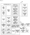
- FIG. 1 illustrates, in block diagram format, an example of an electronic device 101 in a network environment 100 according to various embodiments.
- the electronic device 101 in the network environment 100 may communicate with an electronic device 102 via a first network 198 (e.g., a short-range wireless communication network), or an electronic device 104 or a server 108 via a second network 199 (e.g., a long-range wireless communication network).
- the electronic device 101 may communicate with the electronic device 104 via the server 108.
- the processor 120 may execute, for example, software (e.g., a program 140) to control at least one other component (e.g., a hardware or software component) of the electronic device 101 coupled with the processor 120, and may perform various data processing or computation. According to one embodiment, as at least part of the data processing or computation, the processor 120 may load a command or data received from another component (e.g., the sensor module 176 or the communication module 190) in volatile memory 132, process the command or the data stored in the volatile memory 132, and store resulting data in non-volatile memory 134.
- software e.g., a program 140
- the processor 120 may load a command or data received from another component (e.g., the sensor module 176 or the communication module 190) in volatile memory 132, process the command or the data stored in the volatile memory 132, and store resulting data in non-volatile memory 134.
- the processor 120 may include a main processor 121 (e.g., a central processing unit (CPU) or an application processor (AP)), and an auxiliary processor 123 (e.g., a graphics processing unit (GPU), an image signal processor (ISP), a sensor hub processor, or a communication processor (CP)) that is operable independently from, or in conjunction with, the main processor 121.
- auxiliary processor 123 e.g., a graphics processing unit (GPU), an image signal processor (ISP), a sensor hub processor, or a communication processor (CP)
- the auxiliary processor 123 may be adapted to consume less power than the main processor 121, or to be specific to a specified function.
- the auxiliary processor 123 may be implemented as separate from, or as part of the main processor 121.
- the audio module 170 may convert a sound into an electrical signal and vice versa. According to certain embodiments, the audio module 170 may obtain the sound via the input device 150, or output the sound via the sound output device 155 or a headphone of an external electronic device (e.g., an electronic device 102) directly (e.g., through a physical coupling, such as a wire) or wirelessly coupled with the electronic device 101.
- an external electronic device e.g., an electronic device 102
- directly e.g., through a physical coupling, such as a wire
- the sensor module 176 may detect an operational state (e.g., power or temperature) of the electronic device 101 or an environmental state (e.g., a state of a user) external to the electronic device 101, and then generate an electrical signal or data value corresponding to the detected state.
- the sensor module 176 may include, for example, a gesture sensor, a gyro sensor, an atmospheric pressure sensor, a magnetic sensor, an acceleration sensor, a grip sensor, a proximity sensor, a color sensor, an infrared (IR) sensor, a biometric sensor, a temperature sensor, a humidity sensor, or an illuminance sensor.
- a corresponding one of these communication modules may communicate with the external electronic device via the first network 198 (e.g., a short-range communication network, such as BLUETOOTH TM , wireless-fidelity (WI-FI) direct, or infrared data association (IrDA)) or the second network 199 (e.g., a long-range communication network, such as a cellular network, the Internet, or a computer network (e.g., LAN or wide area network (WAN)).
- the first network 198 e.g., a short-range communication network, such as BLUETOOTH TM , wireless-fidelity (WI-FI) direct, or infrared data association (IrDA)
- the second network 199 e.g., a long-range communication network, such as a cellular network, the Internet, or a computer network (e.g., LAN or wide area network (WAN)
- These various types of communication modules may be implemented as a single component (e.g., a single chip),
- the wireless communication module 192 may identify and authenticate the electronic device 101 in a communication network, such as the first network 198 or the second network 199, using subscriber information (e.g., international mobile subscriber identity (IMSI)) stored in the subscriber identification module 196.
- subscriber information e.g., international mobile subscriber identity (IMSI)
- the signal or the power may then be transmitted or received between the communication module 190 and the external electronic device via the selected at least one antenna.
- another component e.g., a radio frequency integrated circuit (RFIC)
- RFIC radio frequency integrated circuit
- At least some of the above-described components may be coupled mutually and communicate signals (e.g., commands or data) therebetween via an inter-peripheral communication scheme (e.g., a bus, general purpose input and output (GPIO), serial peripheral interface (SPI), or mobile industry processor interface (MIPI)).
- an inter-peripheral communication scheme e.g., a bus, general purpose input and output (GPIO), serial peripheral interface (SPI), or mobile industry processor interface (MIPI)
- FIG. 2 illustrates, in a block diagram 200 , an example of the wireless communication module 192, the power management module 188, and the antenna module 197 of the electronic device 101 according to various embodiments.
- the wireless communication module 192 may include a magnetic secure transmission (MST) communication module 210 or a near-field communication (NFC) module 230
- the power management module 188 may include a wireless charging module 250.
- the antenna module 197 may include a plurality of antennas that include a MST antenna 297-1 connected with the MST communication module 210, a NFC antenna 297-3 connected with the NFC communication module 230, and a wireless charging antenna 297-5 connected with the wireless charging module 250.
- MST magnetic secure transmission
- NFC near-field communication
- the antenna module 197 may include a plurality of antennas that include a MST antenna 297-1 connected with the MST communication module 210, a NFC antenna 297-3 connected with the NFC communication module 230, and a wireless charging antenna 297-5 connected with the
- the second side 110B may be constructed of a rear plate 111 (or a rear cover) which may be opaque.
- the rear plate 111 may be constructed, for example, and without limitation, of coated or colored glass, ceramic, polymer, metallic materials (e.g. aluminum, stainless steel (STS), or magnesium), a combination of at least two of these materials, or the like.
- a recess or opening may be formed in a part of the screen display area of the display 301, and the electronic device(300) may include another electronic components (e.g., a camera module 305, a proximity sensor or an illuminance sensor) aligned with the recess or the opening.
- another electronic components e.g., a camera module 305, a proximity sensor or an illuminance sensor
- the electronic device 300 may generate an electrical signal or data value corresponding to an internal operating state or an external environmental state by including a sensor module.
- the sensor module may include, for example, a proximity sensor disposed on the first surface 310A of the housing 310, a fingerprint sensor integrated or adjacent to the display 301, and/or a biometric sensor (e.g., an HRM sensor) disposed on the second surface 310B.
- the electronic device 300 includes a sensor module, for example, a gesture sensor, a gyro sensor, an air pressure sensor, a magnetic sensor, an acceleration sensor, a grip sensor, a color sensor, an infrared (IR) sensor, a biosensor, a temperature sensor, It may further include at least one of a humidity sensor or an illumination sensor.
- the housing 401 may form an internal space of the electronic device 400.
- the housing 401 may include a lateral bezel structure 410 that forms a lateral side of the electronic device 400.
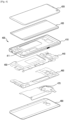
- the FPCB antenna module 501, the shielding member 502, the radiating sheet 503, the bonding member 504, and the printed circuit board 440 may be stacked in the internal space of the housing 401.
- the FPCB antenna module 501 may include an antenna pattern 511 and a nonconductive layer 512 surrounding the antenna pattern 511.
- the near-field communication pattern 511b may be disposed along the periphery of the wireless charging pattern 511a.
- the near-field communication pattern 511b may be patterned on both sides or one side of a base layer.
- the near-field communication pattern 511b may be electrically connected to the printed circuit board.
- the electronic device 400 may transmit and receive a signal to and from an external electronic device through the near-field communication pattern 511b.
- the antenna pattern 511 When an electric current flows through the antenna pattern 511 according to an antenna operation, heat may be generated due to resistance. When the generated heat is not properly radiated, the heat may accumulate in the electronic device 400, thus causing a deterioration in performance. Further, when the housing (e.g., a second side 310B of FIG. 3B ) of the electronic device 400 is heated by the heat generated by the antenna pattern 511, the user may experience discomfort when using the electronic device 400. To discharge the heat generated in the antenna pattern 511, the radiating sheet 503 may be attached to the antenna pattern 511.
- the nonconductive layer 512 may extend from a third region 523 corresponding to the antenna pattern 511 to a first region 521 and a fifth region 525 in which an electronic component is disposed.
- An extended portion of the nonconductive layer 512 may be disposed to overlap the radiating sheet 503 and/or the electronic component.
- the extended portion of the nonconductive layer 512 may be attached to a portion of the electronic component through the bonding member 504.
- the FPCB antenna module 501 may include an additional conductive pattern 513.
- the FPCB antenna module 501 may include the additional conductive pattern 513 in a portion extending to the first region 521 or the fifth region 525.
- the additional conductive pattern 513 may be disposed in first, second, fourth, and fifth regions 521, 522, 524, and 525 of the FPCB antenna module 501.
- the additional conductive pattern 513 may be disposed along the outer boundary of the radiating sheet 503.
- the additional conductive pattern 513 may not function as a conducting wire. In another embodiment, the additional conductive pattern 513 may be electrically connected to the printed circuit board 440.
- the shielding member 502 may be attached to one side of the antenna pattern 511.
- the battery 450, the printed circuit board 440, or the support member 360 may be disposed on one surface of the shielding member 502, and the wireless charging pattern 511a, the near-field communication pattern 511b, or the magnetic secure transmission pattern 511c may be disposed on the other surface of the shielding member 502.
- the shielding member 502 may be formed of a material having a high permeability and a low loss tangent in the band of the near-field communication pattern 511b and the wireless charging pattern 511a.
- the shielding member 502 may include a microcrystalline material and may have a high permeability and a low loss tangent in the band of the near-field communication pattern 511b and the wireless charging pattern 511a of about 10 kHz to 15 MHz. Therefore, the shielding member 502 may be used as a ferromagnetic body in the band of the near-field communication pattern 511b and the wireless charging pattern 511a of about 10 kHz to 15 MHz.
- the printed circuit board 440 may extend from the first region 521 to the fifth region 525 along one edge of the housing 401.
- the electronic component on the printed circuit board 440 may be attached to or may be in contact with one surface of the radiating sheet 503 and/or the FPCB antenna module 501.
- a portion of the radiating sheet 503 may be attached to one surface of the shielding member 502. In certain embodiments, a portion of the radiating sheet 503 may be attached to a portion of the FPCB antenna module 501. In certain embodiments, a portion of the radiating sheet 503 may be attached to a portion of the electronic component. According to certain embodiments, the radiating sheet 503 may extend from the third region 523, where the antenna pattern 511 is disposed, to the first region 521 and/or the fifth region 525, where the electronic device 505 is disposed.
- the radiating sheet 503 is formed of one layer but is not limited thereto. In another embodiment, the radiating sheet 503 may be formed of a plurality of layers. The plurality of layers forming the radiating sheet 503 may have the same thickness, or at least one of the plurality of layers may have a different thickness.
- the bonding member 504 may be disposed between the radiating sheet 503 and the electronic component on the printed circuit board 440. In another embodiment, a portion of the bonding member 504 may be disposed between the FPCB antenna module 501 and the printed circuit board 440, and another portion thereof may be disposed between the printed circuit board 440 and the radiating sheet 503. In still another embodiment, the bonding member 504 may be disposed between the radiating sheet 503 (or the FPCB antenna module 501) and a structure inside the housing 401. Due to the bonding member 504, the FPCB antenna module 501 may be fixed in the housing, thus preventing the FPCB antenna module 501 from moving in the housing.
- the FPCB antenna module 501 may include the nonconductive layer 512 and the antenna pattern 511.
- the antenna pattern 511 and/or the nonconductive layer 512 may be formed of a plurality of layers.
- the antenna pattern 511 may include two layers.
- the FPCB antenna module 501 may extend from the region 523 in which the antenna pattern 511 is disposed to the region 521 in which the electronic component 505, which is an additional heat-generating source, is disposed or to a portion of the region 521.
- the extended portion may include only the nonconductive layer 512 without a conductive pattern (e.g., the antenna pattern 511).
- the shielding member 502 may be disposed on one surface of the FPCB antenna module 501. In certain embodiments, the shielding member 502 may be disposed to overlap the antenna pattern 511 of the FPCB antenna module 501. For example, the shielding member 502 may be attached to a region in which the wireless charging pattern 511a, the near-field communication pattern 511b, and the magnetic secure transmission pattern 511c of the FPCB antenna module 501are positioned.
- the radiating sheet 503 may be disposed in the third region 523, the fourth region 524, and the fifth region 525.
- a portion of the radiating sheet 503 may be attached to the FPCB antenna module 501 and another portion thereof may be attached to the electronic component 505.
- the radiating sheet 503 may be attached to a portion of the electronic component 505.
- the radiating sheet 503 may be disposed across the third to fifth regions 523, 524, and 525, thereby improving the heat radiation performance of the electronic device 400.
- the heat generated by the antenna pattern 511 in the third region 523 may spread not only in the radiating sheet 503 in the third region 523 but also to the radiating sheet in the fourth region 524 and the fifth region 525, thereby being relatively quickly radiated.
- the heat generated by the electronic component 505 in the fifth region 525 may spread not only in the radiating sheet 503 in the fifth region 525 but also to the radiating sheet 503 in the third region 523 and the fourth region 524, thereby being relatively quickly radiated.
- the bonding member 504 may be disposed between the radiating sheet 503 and the electronic component 505.
- the bonding member 504 may fix the FPCB antenna module 501 attached to the radiating sheet 503 in the housing.
- the bonding member 504 may be disposed between the extended FPCB antenna module 501 and the electronic component 505.
- the nonconductive layer 512 when the nonconductive layer 512 extends to the fifth region 525, the nonconductive layer 512 may withstand, along with the radiating sheet 503, stress due to a relative movement between the third region 523 and the fifth region 525.
- the FPCB antenna module 501 may further include an additional conductive pattern 513 in the extended portion. Referring to the non-limiting example of FIG. 11 , the portion of the radiating sheet 503 in the fifth region 525 may be surrounded by the additional conductive pattern 513.
- the nonconductive layer 512 and the further included additional conductive pattern 513 may withstand, along with the radiating sheet 503, stress due to the relative movement between the third region 523 and the fifth region 525. Therefore, damage to the radiating sheet 503 due to a relative movement occurring between the FPCB antenna module 501 and the electronic component 505 may be prevented.
- the FPCB antenna module 501 may include the nonconductive layer 512, the antenna pattern 511, and the additional conductive pattern 513.
- the nonconductive layer 512 of the FPCB antenna module 501 may extend from the third region 523, in which the antenna pattern 511 is formed, to the fifth region 525, in which the electronic component 505, which is an additional heat-generating source, is disposed, or to a portion of the fifth region 525.
- the FPCB antenna module 501 may include the additional conductive pattern 513 in the extended portion.
- the additional conductive pattern 513 may be electrically disconnected from the antenna pattern 511 disposed in the third region.
- the additional conductive pattern 513 may be electrically connected to the printed circuit board 440 so as to function as an electronic component (e.g., an antenna).
- the additional conductive pattern 513 may be disposed at a distance from the radiating sheet 503.
- the additional conductive pattern 513 may be spaced apart from an outer boundary of the radiating sheet 503.
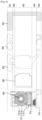
- FIG. 9 illustrates, in cross-sectional view the example FPCB antenna module 501 taken along line C-C' in FIG. 5 .
- the FPCB antenna module 501 may include the nonconductive layer 512, the antenna pattern 511, and the additional conductive pattern 513. In certain embodiments, the FPCB antenna module 501 may extend from the region 523 in which the antenna pattern 511 is formed to the region 525 in which the electronic component 505, which is an additional heat-generating source, is disposed or to a portion of the region 525.
- the FPCB antenna module 501 may include the additional conductive pattern 513 in portions extending to the fourth region 524 and the fifth region 525.
- the additional conductive pattern 513 may be electrically disconnected (d2) from the antenna pattern 511.
- the radiating sheet 503 may be disposed to overlap the FPCB antenna module 501.
- the radiating sheet 503 may be disposed under the shielding member 502 and may receive heat from the FPCB antenna module 501 through the shielding member.
- the radiating sheet 503 may spread the received heat into the radiating sheet 503, thereby preventing the heat from accumulating in the FPCB antenna module 501.
- the bonding member 504 may be disposed between the FPCB antenna module 501 and the electronic component 505.
- the FPCB antenna module 501 is attached to the electronic component 505 in the illustrated embodiment, the embodiment is not limited thereto.
- the FPCB antenna module 501 may be attached to an apparatus inside the housing.
- the bonding member 504 may fix the FPCB antenna module 501 in the housing. By fixing the FPCB antenna module 501 in the housing, the FPCB antenna module 501 may be prevented from moving in the housing, and thus the FPCB antenna module 501 may operate normally.
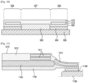
- FIG. 10 illustrates, incross-sectional view, the example FPCB antenna module 501 taken along line D-D' in FIG. 5 .
- the non-limiting example of FIG. 10 shows a cross section of the FPCB antenna module 501 extending from the third region 523 to the fifth region 525, taken in a direction perpendicular to the extending direction.
- the additional conductive pattern 513 may be disposed in a portion of the nonconductive layer 512. According to certain embodiments, the additional conductive pattern 513 may be disposed at a distance from the radiating sheet 503. In certain embodiments, when the FPCB antenna module 501 is viewed from above, the radiating sheet 503 and the additional conductive pattern 513 may not overlap. For example, the radiating sheet 503 may be disposed under a portion 527 of the FPCB antenna module 501 including only the nonconductive layer 512. In certain embodiments, the electronic component 505 may be attached to a portion 526 including the additional conductive pattern 513 through the bonding member 504.
- the thickness of a component in which the radiating sheet 503 and the FPCB antenna module 501 are combined may be kept relatively constant. By reducing the thickness of the component in which the radiating sheet 503 and the FPCB antenna module 501 are combined, the internal space of the housing 500 may be efficiently used.
- the radiating sheet 503 is direct in contact with the electronic component 505 without the bonding member 504, the radiating sheet 503 may be less likely to be damaged when the FPCB antenna module 501 is separated from the electronic component 505.
- FIG. 11 illustrates an example of a modified stacked structure of an FPCB antenna according to certain embodiments.
- FIG. 11 illustrates certain embodiments in which an additional conductive pattern is disposed to overlap a radiating sheet.
- the FPCB antenna module 1210 may include a nonconductive layer 1212, an antenna pattern 1211, and an additional conductive pattern 1213. In certain embodiments, the FPCB antenna module 1210 may extend from a region in which the conductive pattern 12111 is formed to a region in which an electronic component 1150, which is an additional heat-generating source, is disposed.
- a shielding member 1120 may be disposed on one surface of the FPCB antenna module 1210.
- the shielding member 1120 may be attached to a region corresponding to the conductive pattern 1111 of the FPCB antenna module 1210.
- a portion of a radiating sheet 1130 may be attached to the FPCB antenna module 12110, and another portion thereof may be attached to the electronic component 1150.
- the radiating sheet 1130 may extend from the region in which the conductive pattern 1211 of the FPCB antenna module 1210 is disposed to the region in which the electronic component 1150 is disposed.
- the heat radiation performance of the radiating sheet 1130 may be improved.
- the heat generated by the antenna pattern 1211 may spread not only in the radiating sheet 1130 in the region corresponding to the antenna pattern 1211 but also to the radiating sheet 1130 in the region in which the electronic component 1150 is disposed, thereby being relatively quickly radiated.
- a bonding member 1140 may be disposed between the radiating sheet 1130 and the electronic component 1150.
- the bonding member 1140 may fix the FPCB antenna module 1210 disposed on the radiating sheet 1130 in a housing. By fixing the FPCB antenna module 1210 in the housing, the FPCB antenna module 1210 may be prevented from moving in the housing.
- the nonconductive layer 1212 of the FPCB antenna module 1210 may extend to the region in which the electronic component 1150 is disposed.
- the FPCB antenna module 1210 may further include the additional conductive pattern 1213 in the extended portion.
- the additional conductive pattern 1213 may overlap the radiating sheet 1130.
- the FPCB antenna module 1110 including the nonconductive layer 1212 and the additional conductive pattern 1213 may withstand, along with the radiating sheet 1130, stress caused by a relative movement between the FPCB antenna module 1210 and the electronic component 1150.
Landscapes
- Engineering & Computer Science (AREA)
- Microelectronics & Electronic Packaging (AREA)
- Computer Networks & Wireless Communication (AREA)
- Signal Processing (AREA)
- Physics & Mathematics (AREA)
- Electromagnetism (AREA)
- Theoretical Computer Science (AREA)
- Computer Hardware Design (AREA)
- Manufacturing & Machinery (AREA)
- Power Engineering (AREA)
- General Physics & Mathematics (AREA)
- General Engineering & Computer Science (AREA)
- Human Computer Interaction (AREA)
- Telephone Function (AREA)
- Telephone Set Structure (AREA)
Claims (15)
- Elektronische Vorrichtung (400), die Folgendes umfasst:ein Gehäuse (401), das so konfiguriert ist, dass es einen Innenraum bildet;eine Strahlungsplatte (503), die so konfiguriert ist, dass sie in dem Innenraum angeordnet werden kann;mindestens eine elektronische Komponente (505), die so konfiguriert ist, dass sie in dem Innenraum angeordnet und mit der Strahlungsplatte (503) verbunden werden kann; undein flexibles Leiterplatten-, FPCB-,Antennenmodul (501), das so konfiguriert ist, dass es auf der Strahlungsplatte (503) angeordnet werden kann und ein Antennenmuster (511) und eine nichtleitende Schicht (512) umfasst, wobei die nichtleitende Schicht (512) so konfiguriert ist, dass sie das Antennenmuster (511) umgibt,wobei sich die nichtleitende Schicht (512) bis zu einem Bereich erstreckt, in dem die elektronische Komponente (505) positioniert ist.
- Elektronische Vorrichtung nach Anspruch 1, die ferner Folgendes umfasst:
ein abschirmendes Element (502), das so konfiguriert ist, dass es zwischen der Strahlungsplatte (503) und dem FPCB-Antennenmodul (501) gestapelt werden kann. - Elektronische Vorrichtung nach Anspruch 1, die ferner Folgendes umfasst:
ein Verbindungselement (504), das so konfiguriert ist, dass es zwischen der Strahlungsplatte (503) und der elektronischen Komponente (505) angeordnet werden kann. - Elektronische Vorrichtung nach Anspruch 1, die ferner Folgendes umfasst:
ein Verbindungselement (504), das so konfiguriert ist, dass es zwischen dem FPCB-Antennenmodul (501) und der elektronischen Komponente (505) angeordnet werden kann. - Elektronische Vorrichtung nach Anspruch 1, wobei das FPCB-Antennenmodul (501) ferner ein zusätzliches leitfähiges Muster (513) in einem Abschnitt aufweist, der sich bis zu der elektronischen Komponente (505) erstreckt.
- Elektronische Vorrichtung nach Anspruch 5, wobei sich das zusätzliche leitfähige Muster (513) von einem an das Antennenmuster (511) angrenzenden Bereich bis zu dem Bereich erstreckt, in dem die elektronische Komponente (505) positioniert ist.
- Elektronische Vorrichtung nach Anspruch 5, wobei das zusätzliche leitfähige Muster (513) elektrisch von dem Antennenmuster (511) getrennt ist.
- Elektronische Vorrichtung nach Anspruch 5, wobei das zusätzliche leitfähige Muster (513) von einer Begrenzung der Strahlungsplatte (503) beabstandet ist, wenn das FPCB-Antennenmodul (501) von oben betrachtet wird.
- Elektronische Vorrichtung nach Anspruch 5, wobei das zusätzliche leitfähige Muster (513) entlang einer Begrenzung des Abschnitts des FPCB-Antennenmoduls (501) ausgebildet ist, der sich bis zu der elektronischen Komponente (505) erstreckt.
- Elektronische Vorrichtung nach Anspruch 1, wobei das Antennenmuster (511) eine Antenne umfasst, die als mindestens eines von einem Nahfeldkommunikations-, NFC-,Muster oder einem sicheren magnetischen Übertragungs-, MST-,Muster arbeitet.
- Elektronische Vorrichtung nach Anspruch 1, wobei das FPCB-Antennenmodul (501) auf einer Oberfläche der Strahlungsplatte (503) angeordnet ist und die elektronische Komponente (505) auf einer Oberfläche angeordnet ist, die in eine andere Richtung als die Oberfläche der Strahlungsplatte (503) weist.
- Elektronische Vorrichtung nach Anspruch 1, wobei die elektronische Komponente (505) ferner einen Abschnitt einer Leiterplatte, PCB, (440) umfasst.
- Elektronische Vorrichtung nach Anspruch 1, wobei die Strahlungsplatte (503) eine Stufe zwischen einem an dem Antennenmuster (511) befestigten Abschnitt und einem an der elektronischen Komponente (1150) befestigten Abschnitt umfasst.
- Elektronische Vorrichtung nach Anspruch 1, die ferner Folgendes umfasst:
ein Verbindungselement (504), das so konfiguriert ist, dass es zwischen einer Struktur im Gehäuse (401) und einem erweiterten Abschnitt des FPCB-Antennenmoduls (501) angeordnet wird. - Elektronische Vorrichtung nach Anspruch 1, bei der ein Abschnitt der elektronischen Komponente (1150) an der Strahlungsplatte (503) befestigt ist und ein anderer Abschnitt davon an einem erweiterten Abschnitt des FPCB-Antennenmoduls (501) befestigt ist.
Applications Claiming Priority (2)
| Application Number | Priority Date | Filing Date | Title |
|---|---|---|---|
| KR1020190035389A KR102613670B1 (ko) | 2019-03-27 | 2019-03-27 | 연장된 fpcb 안테나 모듈을 포함하는 전자 장치 |
| PCT/KR2020/004273 WO2020197345A1 (en) | 2019-03-27 | 2020-03-27 | Electronic device including expanded flexible printed circuit board antenna module |
Publications (3)
| Publication Number | Publication Date |
|---|---|
| EP3903377A1 EP3903377A1 (de) | 2021-11-03 |
| EP3903377A4 EP3903377A4 (de) | 2022-03-02 |
| EP3903377B1 true EP3903377B1 (de) | 2024-07-03 |
Family
ID=72603673
Family Applications (1)
| Application Number | Title | Priority Date | Filing Date |
|---|---|---|---|
| EP20778501.5A Active EP3903377B1 (de) | 2019-03-27 | 2020-03-27 | Elektronische vorrichtung mit erweitertem flexiblen leiterplattenantennenmodul |
Country Status (5)
| Country | Link |
|---|---|
| US (1) | US11431083B2 (de) |
| EP (1) | EP3903377B1 (de) |
| KR (1) | KR102613670B1 (de) |
| CN (1) | CN113632316B (de) |
| WO (1) | WO2020197345A1 (de) |
Families Citing this family (9)
| Publication number | Priority date | Publication date | Assignee | Title |
|---|---|---|---|---|
| KR102847031B1 (ko) | 2020-12-21 | 2025-08-20 | 삼성전자주식회사 | 코일 안테나를 포함하는 전자 장치 |
| KR102919981B1 (ko) * | 2021-02-03 | 2026-01-30 | 삼성전자주식회사 | 안테나 패턴을 포함하는 플렉서블 어셈블리 및 이를 포함하는 전자 장치 |
| BR112023020782A2 (pt) | 2021-04-06 | 2023-12-12 | Samsung Electronics Co Ltd | Dispositivo eletrônico incluindo estrutura de dissipação de calor |
| KR102893336B1 (ko) * | 2021-04-06 | 2025-12-01 | 삼성전자주식회사 | 방열 구조를 포함하는 전자 장치 |
| KR20230005630A (ko) | 2021-07-01 | 2023-01-10 | 삼성전자주식회사 | 안테나를 포함하는 전자 장치 |
| US11777218B2 (en) * | 2021-12-27 | 2023-10-03 | Google Llc | Antenna design with structurally integrated composite antenna components |
| US20230299165A1 (en) * | 2022-03-15 | 2023-09-21 | Intel Corporation | Fabrication of gate-all-around integrated circuit structures having pre-spacer-deposition wide cut gates with non-merged spacers |
| US20230352823A1 (en) * | 2022-04-28 | 2023-11-02 | Meta Platforms Technologies, Llc | Flexible printed circuit board with near-field communication (nfc) coil integration |
| EP4679626A1 (de) | 2023-07-10 | 2026-01-14 | Samsung Electronics Co., Ltd. | Elektronische vorrichtung mit antennenmodul |
Family Cites Families (23)
| Publication number | Priority date | Publication date | Assignee | Title |
|---|---|---|---|---|
| JP5051189B2 (ja) | 2009-07-10 | 2012-10-17 | アイシン・エィ・ダブリュ株式会社 | 電子回路装置 |
| KR101570617B1 (ko) | 2014-09-05 | 2015-11-20 | 엘지디스플레이 주식회사 | 연성회로기판 및 그를 구비하는 터치패널 |
| KR101643928B1 (ko) * | 2014-11-26 | 2016-07-29 | (주)파트론 | 안테나 구조체 |
| KR20160090144A (ko) * | 2015-01-21 | 2016-07-29 | 주식회사 아모그린텍 | 방열 시트 일체형 안테나 모듈 |
| KR102294019B1 (ko) * | 2015-01-28 | 2021-08-26 | 삼성전자주식회사 | 안테나 장치 및 그것을 포함하는 전자 장치 |
| KR102314790B1 (ko) * | 2015-02-26 | 2021-10-20 | 삼성전자주식회사 | 안테나 장치를 포함하는 전자 장치 |
| CN204596965U (zh) | 2015-05-12 | 2015-08-26 | 深圳市嘉姆特科技有限公司 | 一种多功能nfc天线 |
| KR102342852B1 (ko) | 2015-06-16 | 2021-12-23 | 삼성전자주식회사 | 무선 통신 모듈, 이를 포함하는 휴대 단말기 |
| KR101609642B1 (ko) * | 2015-07-10 | 2016-04-08 | 주식회사 아모그린텍 | Nfc 안테나 일체형 방열시트 및 이를 구비하는 휴대단말기 |
| KR102487477B1 (ko) * | 2016-01-20 | 2023-01-12 | 삼성전자주식회사 | 디스플레이를 이용한 안테나 |
| KR102567364B1 (ko) * | 2016-01-27 | 2023-08-16 | 삼성전자주식회사 | 안테나 보조 장치 및 이를 포함하는 전자 장치 |
| CN205622671U (zh) * | 2016-03-18 | 2016-10-05 | 上海与德通讯技术有限公司 | 一种移动终端 |
| WO2017183910A2 (en) * | 2016-04-19 | 2017-10-26 | Samsung Electronics Co., Ltd. | Electronic device supporting fingerprint verification and method for operating the same |
| KR102466002B1 (ko) * | 2016-04-19 | 2022-11-11 | 삼성전자주식회사 | 안테나를 포함하는 전자 장치 |
| KR102497472B1 (ko) | 2016-07-29 | 2023-02-08 | 삼성전자주식회사 | 방수 구조를 포함하는 전자 장치 |
| KR102483238B1 (ko) | 2016-08-01 | 2022-12-30 | 삼성전자 주식회사 | 방열 장치 및 이를 구비하는 전자 장치 |
| KR102621757B1 (ko) * | 2016-09-07 | 2024-01-08 | 삼성전자주식회사 | 무선 통신을 위한 안테나 및 이를 포함하는 전자 장치 |
| US10691995B2 (en) * | 2016-09-23 | 2020-06-23 | Amotech Co., Ltd. | Antenna module |
| KR102335846B1 (ko) * | 2017-04-17 | 2021-12-07 | 삼성전자주식회사 | 복수의 코일들을 포함하는 전자 장치 |
| US10720695B2 (en) * | 2017-05-15 | 2020-07-21 | Speedlink Technology Inc. | Near field communication antenna modules for devices with metal frame |
| KR20190006343A (ko) * | 2017-07-10 | 2019-01-18 | 송영석 | 방열 무선통신 안테나 구조 |
| US10141625B1 (en) * | 2017-07-13 | 2018-11-27 | Lg Electronics Inc. | Mobile terminal |
| KR102514547B1 (ko) * | 2018-07-16 | 2023-03-27 | 삼성전자주식회사 | 안테나를 포함하는 디스플레이 조립체 및 이를 포함하는 전자 장치 |
-
2019
- 2019-03-27 KR KR1020190035389A patent/KR102613670B1/ko active Active
-
2020
- 2020-03-27 CN CN202080024587.3A patent/CN113632316B/zh active Active
- 2020-03-27 WO PCT/KR2020/004273 patent/WO2020197345A1/en not_active Ceased
- 2020-03-27 US US16/833,170 patent/US11431083B2/en active Active
- 2020-03-27 EP EP20778501.5A patent/EP3903377B1/de active Active
Also Published As
| Publication number | Publication date |
|---|---|
| CN113632316B (zh) | 2024-09-10 |
| KR102613670B1 (ko) | 2023-12-14 |
| CN113632316A (zh) | 2021-11-09 |
| KR20200114150A (ko) | 2020-10-07 |
| WO2020197345A1 (en) | 2020-10-01 |
| EP3903377A1 (de) | 2021-11-03 |
| US20200313284A1 (en) | 2020-10-01 |
| EP3903377A4 (de) | 2022-03-02 |
| US11431083B2 (en) | 2022-08-30 |
Similar Documents
| Publication | Publication Date | Title |
|---|---|---|
| EP3903377B1 (de) | Elektronische vorrichtung mit erweitertem flexiblen leiterplattenantennenmodul | |
| US11886238B2 (en) | Foldable electronic device | |
| KR102651418B1 (ko) | 차폐 시트 및 방열 부재를 포함하는 전자 장치 | |
| KR102659482B1 (ko) | 인터포저를 포함하는 전자 장치 | |
| US10854958B2 (en) | Electronic device including grip sensor and antenna | |
| US11019736B2 (en) | Electronic device including flexible printed circuit board | |
| US11665818B2 (en) | Electronic device including flexible printed circuit board laminated wireless charging coil and near field communication antenna pattern | |
| US10965157B2 (en) | Electronic device having a plurality of stacked coil antennas | |
| EP3794808B1 (de) | Elektronische vorrichtung mit einer an die antenne angrenzenden flexiblen leiterplatte | |
| US12395578B2 (en) | Electronic device comprising housing | |
| US11825007B2 (en) | Component stack mounting structure and electronic device including same | |
| US11258174B2 (en) | Antenna radiator including plurality of layers and electronic device including the same | |
| US12250798B2 (en) | Electronic device including heat dissipation sheet | |
| US20200127382A1 (en) | Electronic device including antenna apparatus using photo-conductive material and antenna control method | |
| EP4333568B1 (de) | Starre flexible leiterplatte und elektronische vorrichtung damit | |
| US12272864B2 (en) | Electronic device including antenna | |
| US20240332797A1 (en) | Antenna structure and electronic device including same | |
| EP4629038A1 (de) | Anzeigemodul mit struktur zur reduzierung von schäden und elektronische vorrichtung damit | |
| EP4510380A1 (de) | Antenne und elektronische vorrichtung mit antenne | |
| US20250338396A1 (en) | Electronic device comprising flexible printed circuit board | |
| KR20240145843A (ko) | 안테나 구조 및 이를 포함하는 전자 장치 | |
| KR20230055245A (ko) | 무선충전 코일 및 이를 포함하는 전자 장치 |
Legal Events
| Date | Code | Title | Description |
|---|---|---|---|
| STAA | Information on the status of an ep patent application or granted ep patent |
Free format text: STATUS: THE INTERNATIONAL PUBLICATION HAS BEEN MADE |
|
| PUAI | Public reference made under article 153(3) epc to a published international application that has entered the european phase |
Free format text: ORIGINAL CODE: 0009012 |
|
| STAA | Information on the status of an ep patent application or granted ep patent |
Free format text: STATUS: REQUEST FOR EXAMINATION WAS MADE |
|
| 17P | Request for examination filed |
Effective date: 20210727 |
|
| AK | Designated contracting states |
Kind code of ref document: A1 Designated state(s): AL AT BE BG CH CY CZ DE DK EE ES FI FR GB GR HR HU IE IS IT LI LT LU LV MC MK MT NL NO PL PT RO RS SE SI SK SM TR |
|
| A4 | Supplementary search report drawn up and despatched |
Effective date: 20220131 |
|
| RIC1 | Information provided on ipc code assigned before grant |
Ipc: G06F 1/20 20060101ALI20220125BHEP Ipc: H01Q 1/24 20060101ALI20220125BHEP Ipc: H01Q 1/22 20060101ALI20220125BHEP Ipc: H01Q 1/02 20060101AFI20220125BHEP |
|
| DAV | Request for validation of the european patent (deleted) | ||
| DAX | Request for extension of the european patent (deleted) | ||
| GRAP | Despatch of communication of intention to grant a patent |
Free format text: ORIGINAL CODE: EPIDOSNIGR1 |
|
| STAA | Information on the status of an ep patent application or granted ep patent |
Free format text: STATUS: GRANT OF PATENT IS INTENDED |
|
| INTG | Intention to grant announced |
Effective date: 20240208 |
|
| RIN1 | Information on inventor provided before grant (corrected) |
Inventor name: KIM, HOJONG Inventor name: KEUM, KYEONGJO Inventor name: KIM, YOUNJU |
|
| GRAS | Grant fee paid |
Free format text: ORIGINAL CODE: EPIDOSNIGR3 |
|
| GRAA | (expected) grant |
Free format text: ORIGINAL CODE: 0009210 |
|
| STAA | Information on the status of an ep patent application or granted ep patent |
Free format text: STATUS: THE PATENT HAS BEEN GRANTED |
|
| AK | Designated contracting states |
Kind code of ref document: B1 Designated state(s): AL AT BE BG CH CY CZ DE DK EE ES FI FR GB GR HR HU IE IS IT LI LT LU LV MC MK MT NL NO PL PT RO RS SE SI SK SM TR |
|
| REG | Reference to a national code |
Ref country code: CH Ref legal event code: EP |
|
| REG | Reference to a national code |
Ref country code: DE Ref legal event code: R096 Ref document number: 602020033412 Country of ref document: DE |
|
| REG | Reference to a national code |
Ref country code: NL Ref legal event code: FP |
|
| REG | Reference to a national code |
Ref country code: LT Ref legal event code: MG9D |
|
| PG25 | Lapsed in a contracting state [announced via postgrant information from national office to epo] |
Ref country code: PT Free format text: LAPSE BECAUSE OF FAILURE TO SUBMIT A TRANSLATION OF THE DESCRIPTION OR TO PAY THE FEE WITHIN THE PRESCRIBED TIME-LIMIT Effective date: 20241104 |
|
| REG | Reference to a national code |
Ref country code: AT Ref legal event code: MK05 Ref document number: 1700808 Country of ref document: AT Kind code of ref document: T Effective date: 20240703 |
|
| PG25 | Lapsed in a contracting state [announced via postgrant information from national office to epo] |
Ref country code: PT Free format text: LAPSE BECAUSE OF FAILURE TO SUBMIT A TRANSLATION OF THE DESCRIPTION OR TO PAY THE FEE WITHIN THE PRESCRIBED TIME-LIMIT Effective date: 20241104 |
|
| PG25 | Lapsed in a contracting state [announced via postgrant information from national office to epo] |
Ref country code: NO Free format text: LAPSE BECAUSE OF FAILURE TO SUBMIT A TRANSLATION OF THE DESCRIPTION OR TO PAY THE FEE WITHIN THE PRESCRIBED TIME-LIMIT Effective date: 20241003 |
|
| PG25 | Lapsed in a contracting state [announced via postgrant information from national office to epo] |
Ref country code: GR Free format text: LAPSE BECAUSE OF FAILURE TO SUBMIT A TRANSLATION OF THE DESCRIPTION OR TO PAY THE FEE WITHIN THE PRESCRIBED TIME-LIMIT Effective date: 20241004 Ref country code: FI Free format text: LAPSE BECAUSE OF FAILURE TO SUBMIT A TRANSLATION OF THE DESCRIPTION OR TO PAY THE FEE WITHIN THE PRESCRIBED TIME-LIMIT Effective date: 20240703 Ref country code: PL Free format text: LAPSE BECAUSE OF FAILURE TO SUBMIT A TRANSLATION OF THE DESCRIPTION OR TO PAY THE FEE WITHIN THE PRESCRIBED TIME-LIMIT Effective date: 20240703 |
|
| PG25 | Lapsed in a contracting state [announced via postgrant information from national office to epo] |
Ref country code: BG Free format text: LAPSE BECAUSE OF FAILURE TO SUBMIT A TRANSLATION OF THE DESCRIPTION OR TO PAY THE FEE WITHIN THE PRESCRIBED TIME-LIMIT Effective date: 20240703 |
|
| PG25 | Lapsed in a contracting state [announced via postgrant information from national office to epo] |
Ref country code: LV Free format text: LAPSE BECAUSE OF FAILURE TO SUBMIT A TRANSLATION OF THE DESCRIPTION OR TO PAY THE FEE WITHIN THE PRESCRIBED TIME-LIMIT Effective date: 20240703 |
|
| PG25 | Lapsed in a contracting state [announced via postgrant information from national office to epo] |
Ref country code: IS Free format text: LAPSE BECAUSE OF FAILURE TO SUBMIT A TRANSLATION OF THE DESCRIPTION OR TO PAY THE FEE WITHIN THE PRESCRIBED TIME-LIMIT Effective date: 20241103 Ref country code: AT Free format text: LAPSE BECAUSE OF FAILURE TO SUBMIT A TRANSLATION OF THE DESCRIPTION OR TO PAY THE FEE WITHIN THE PRESCRIBED TIME-LIMIT Effective date: 20240703 |
|
| PG25 | Lapsed in a contracting state [announced via postgrant information from national office to epo] |
Ref country code: CZ Free format text: LAPSE BECAUSE OF FAILURE TO SUBMIT A TRANSLATION OF THE DESCRIPTION OR TO PAY THE FEE WITHIN THE PRESCRIBED TIME-LIMIT Effective date: 20240703 Ref country code: HR Free format text: LAPSE BECAUSE OF FAILURE TO SUBMIT A TRANSLATION OF THE DESCRIPTION OR TO PAY THE FEE WITHIN THE PRESCRIBED TIME-LIMIT Effective date: 20240703 |
|
| PG25 | Lapsed in a contracting state [announced via postgrant information from national office to epo] |
Ref country code: ES Free format text: LAPSE BECAUSE OF FAILURE TO SUBMIT A TRANSLATION OF THE DESCRIPTION OR TO PAY THE FEE WITHIN THE PRESCRIBED TIME-LIMIT Effective date: 20240703 Ref country code: RS Free format text: LAPSE BECAUSE OF FAILURE TO SUBMIT A TRANSLATION OF THE DESCRIPTION OR TO PAY THE FEE WITHIN THE PRESCRIBED TIME-LIMIT Effective date: 20241003 |
|
| PG25 | Lapsed in a contracting state [announced via postgrant information from national office to epo] |
Ref country code: RS Free format text: LAPSE BECAUSE OF FAILURE TO SUBMIT A TRANSLATION OF THE DESCRIPTION OR TO PAY THE FEE WITHIN THE PRESCRIBED TIME-LIMIT Effective date: 20241003 Ref country code: PL Free format text: LAPSE BECAUSE OF FAILURE TO SUBMIT A TRANSLATION OF THE DESCRIPTION OR TO PAY THE FEE WITHIN THE PRESCRIBED TIME-LIMIT Effective date: 20240703 Ref country code: NO Free format text: LAPSE BECAUSE OF FAILURE TO SUBMIT A TRANSLATION OF THE DESCRIPTION OR TO PAY THE FEE WITHIN THE PRESCRIBED TIME-LIMIT Effective date: 20241003 Ref country code: LV Free format text: LAPSE BECAUSE OF FAILURE TO SUBMIT A TRANSLATION OF THE DESCRIPTION OR TO PAY THE FEE WITHIN THE PRESCRIBED TIME-LIMIT Effective date: 20240703 Ref country code: IS Free format text: LAPSE BECAUSE OF FAILURE TO SUBMIT A TRANSLATION OF THE DESCRIPTION OR TO PAY THE FEE WITHIN THE PRESCRIBED TIME-LIMIT Effective date: 20241103 Ref country code: HR Free format text: LAPSE BECAUSE OF FAILURE TO SUBMIT A TRANSLATION OF THE DESCRIPTION OR TO PAY THE FEE WITHIN THE PRESCRIBED TIME-LIMIT Effective date: 20240703 Ref country code: GR Free format text: LAPSE BECAUSE OF FAILURE TO SUBMIT A TRANSLATION OF THE DESCRIPTION OR TO PAY THE FEE WITHIN THE PRESCRIBED TIME-LIMIT Effective date: 20241004 Ref country code: FI Free format text: LAPSE BECAUSE OF FAILURE TO SUBMIT A TRANSLATION OF THE DESCRIPTION OR TO PAY THE FEE WITHIN THE PRESCRIBED TIME-LIMIT Effective date: 20240703 Ref country code: ES Free format text: LAPSE BECAUSE OF FAILURE TO SUBMIT A TRANSLATION OF THE DESCRIPTION OR TO PAY THE FEE WITHIN THE PRESCRIBED TIME-LIMIT Effective date: 20240703 Ref country code: CZ Free format text: LAPSE BECAUSE OF FAILURE TO SUBMIT A TRANSLATION OF THE DESCRIPTION OR TO PAY THE FEE WITHIN THE PRESCRIBED TIME-LIMIT Effective date: 20240703 Ref country code: BG Free format text: LAPSE BECAUSE OF FAILURE TO SUBMIT A TRANSLATION OF THE DESCRIPTION OR TO PAY THE FEE WITHIN THE PRESCRIBED TIME-LIMIT Effective date: 20240703 Ref country code: AT Free format text: LAPSE BECAUSE OF FAILURE TO SUBMIT A TRANSLATION OF THE DESCRIPTION OR TO PAY THE FEE WITHIN THE PRESCRIBED TIME-LIMIT Effective date: 20240703 |
|
| REG | Reference to a national code |
Ref country code: DE Ref legal event code: R097 Ref document number: 602020033412 Country of ref document: DE |
|
| PG25 | Lapsed in a contracting state [announced via postgrant information from national office to epo] |
Ref country code: RO Free format text: LAPSE BECAUSE OF FAILURE TO SUBMIT A TRANSLATION OF THE DESCRIPTION OR TO PAY THE FEE WITHIN THE PRESCRIBED TIME-LIMIT Effective date: 20240703 Ref country code: DK Free format text: LAPSE BECAUSE OF FAILURE TO SUBMIT A TRANSLATION OF THE DESCRIPTION OR TO PAY THE FEE WITHIN THE PRESCRIBED TIME-LIMIT Effective date: 20240703 Ref country code: SM Free format text: LAPSE BECAUSE OF FAILURE TO SUBMIT A TRANSLATION OF THE DESCRIPTION OR TO PAY THE FEE WITHIN THE PRESCRIBED TIME-LIMIT Effective date: 20240703 |
|
| PG25 | Lapsed in a contracting state [announced via postgrant information from national office to epo] |
Ref country code: EE Free format text: LAPSE BECAUSE OF FAILURE TO SUBMIT A TRANSLATION OF THE DESCRIPTION OR TO PAY THE FEE WITHIN THE PRESCRIBED TIME-LIMIT Effective date: 20240703 |
|
| PG25 | Lapsed in a contracting state [announced via postgrant information from national office to epo] |
Ref country code: IT Free format text: LAPSE BECAUSE OF FAILURE TO SUBMIT A TRANSLATION OF THE DESCRIPTION OR TO PAY THE FEE WITHIN THE PRESCRIBED TIME-LIMIT Effective date: 20240703 Ref country code: SK Free format text: LAPSE BECAUSE OF FAILURE TO SUBMIT A TRANSLATION OF THE DESCRIPTION OR TO PAY THE FEE WITHIN THE PRESCRIBED TIME-LIMIT Effective date: 20240703 |
|
| PLBE | No opposition filed within time limit |
Free format text: ORIGINAL CODE: 0009261 |
|
| STAA | Information on the status of an ep patent application or granted ep patent |
Free format text: STATUS: NO OPPOSITION FILED WITHIN TIME LIMIT |
|
| 26N | No opposition filed |
Effective date: 20250404 |
|
| PG25 | Lapsed in a contracting state [announced via postgrant information from national office to epo] |
Ref country code: SE Free format text: LAPSE BECAUSE OF FAILURE TO SUBMIT A TRANSLATION OF THE DESCRIPTION OR TO PAY THE FEE WITHIN THE PRESCRIBED TIME-LIMIT Effective date: 20240703 |
|
| PG25 | Lapsed in a contracting state [announced via postgrant information from national office to epo] |
Ref country code: MC Free format text: LAPSE BECAUSE OF FAILURE TO SUBMIT A TRANSLATION OF THE DESCRIPTION OR TO PAY THE FEE WITHIN THE PRESCRIBED TIME-LIMIT Effective date: 20240703 |
|
| REG | Reference to a national code |
Ref country code: CH Ref legal event code: H13 Free format text: ST27 STATUS EVENT CODE: U-0-0-H10-H13 (AS PROVIDED BY THE NATIONAL OFFICE) Effective date: 20251023 |
|
| PG25 | Lapsed in a contracting state [announced via postgrant information from national office to epo] |
Ref country code: LU Free format text: LAPSE BECAUSE OF NON-PAYMENT OF DUE FEES Effective date: 20250327 |
|
| REG | Reference to a national code |
Ref country code: BE Ref legal event code: MM Effective date: 20250331 |
|
| PG25 | Lapsed in a contracting state [announced via postgrant information from national office to epo] |
Ref country code: FR Free format text: LAPSE BECAUSE OF NON-PAYMENT OF DUE FEES Effective date: 20250331 |
|
| PG25 | Lapsed in a contracting state [announced via postgrant information from national office to epo] |
Ref country code: BE Free format text: LAPSE BECAUSE OF NON-PAYMENT OF DUE FEES Effective date: 20250331 |
|
| PG25 | Lapsed in a contracting state [announced via postgrant information from national office to epo] |
Ref country code: CH Free format text: LAPSE BECAUSE OF NON-PAYMENT OF DUE FEES Effective date: 20250331 |
|
| PG25 | Lapsed in a contracting state [announced via postgrant information from national office to epo] |
Ref country code: IE Free format text: LAPSE BECAUSE OF NON-PAYMENT OF DUE FEES Effective date: 20250327 |
|
| PGFP | Annual fee paid to national office [announced via postgrant information from national office to epo] |
Ref country code: NL Payment date: 20260220 Year of fee payment: 7 |
|
| PGFP | Annual fee paid to national office [announced via postgrant information from national office to epo] |
Ref country code: GB Payment date: 20260224 Year of fee payment: 7 |
|
| PGFP | Annual fee paid to national office [announced via postgrant information from national office to epo] |
Ref country code: DE Payment date: 20260220 Year of fee payment: 7 |