EP3904292A1 - Supraleitender oxiddraht und verfahren zur herstellung davon - Google Patents
Supraleitender oxiddraht und verfahren zur herstellung davon Download PDFInfo
- Publication number
- EP3904292A1 EP3904292A1 EP19902603.0A EP19902603A EP3904292A1 EP 3904292 A1 EP3904292 A1 EP 3904292A1 EP 19902603 A EP19902603 A EP 19902603A EP 3904292 A1 EP3904292 A1 EP 3904292A1
- Authority
- EP
- European Patent Office
- Prior art keywords
- superconducting layer
- superconducting
- deposition rate
- layer
- artificial pinning
- Prior art date
- Legal status (The legal status is an assumption and is not a legal conclusion. Google has not performed a legal analysis and makes no representation as to the accuracy of the status listed.)
- Withdrawn
Links
Images


Classifications
-
- H—ELECTRICITY
- H01—ELECTRIC ELEMENTS
- H01B—CABLES; CONDUCTORS; INSULATORS; SELECTION OF MATERIALS FOR THEIR CONDUCTIVE, INSULATING OR DIELECTRIC PROPERTIES
- H01B1/00—Conductors or conductive bodies characterised by the conductive materials; Selection of materials as conductors
- H01B1/06—Conductors or conductive bodies characterised by the conductive materials; Selection of materials as conductors mainly consisting of other non-metallic substances
- H01B1/08—Conductors or conductive bodies characterised by the conductive materials; Selection of materials as conductors mainly consisting of other non-metallic substances oxides
-
- C—CHEMISTRY; METALLURGY
- C01—INORGANIC CHEMISTRY
- C01G—COMPOUNDS CONTAINING METALS NOT COVERED BY SUBCLASSES C01D OR C01F
- C01G19/00—Compounds of tin
-
- C—CHEMISTRY; METALLURGY
- C01—INORGANIC CHEMISTRY
- C01G—COMPOUNDS CONTAINING METALS NOT COVERED BY SUBCLASSES C01D OR C01F
- C01G25/00—Compounds of zirconium
-
- C—CHEMISTRY; METALLURGY
- C01—INORGANIC CHEMISTRY
- C01G—COMPOUNDS CONTAINING METALS NOT COVERED BY SUBCLASSES C01D OR C01F
- C01G27/00—Compounds of hafnium
-
- C—CHEMISTRY; METALLURGY
- C01—INORGANIC CHEMISTRY
- C01G—COMPOUNDS CONTAINING METALS NOT COVERED BY SUBCLASSES C01D OR C01F
- C01G3/00—Compounds of copper
- C01G3/006—Compounds containing copper, with or without oxygen or hydrogen, and containing two or more other elements
-
- C—CHEMISTRY; METALLURGY
- C04—CEMENTS; CONCRETE; ARTIFICIAL STONE; CERAMICS; REFRACTORIES
- C04B—LIME, MAGNESIA; SLAG; CEMENTS; COMPOSITIONS THEREOF, e.g. MORTARS, CONCRETE OR LIKE BUILDING MATERIALS; ARTIFICIAL STONE; CERAMICS; REFRACTORIES; TREATMENT OF NATURAL STONE
- C04B35/00—Shaped ceramic products characterised by their composition; Ceramics compositions; Processing powders of inorganic compounds preparatory to the manufacturing of ceramic products
- C04B35/01—Shaped ceramic products characterised by their composition; Ceramics compositions; Processing powders of inorganic compounds preparatory to the manufacturing of ceramic products based on oxide ceramics
- C04B35/45—Shaped ceramic products characterised by their composition; Ceramics compositions; Processing powders of inorganic compounds preparatory to the manufacturing of ceramic products based on oxide ceramics based on copper oxide or solid solutions thereof with other oxides
- C04B35/4504—Shaped ceramic products characterised by their composition; Ceramics compositions; Processing powders of inorganic compounds preparatory to the manufacturing of ceramic products based on oxide ceramics based on copper oxide or solid solutions thereof with other oxides containing rare earth oxides
-
- C—CHEMISTRY; METALLURGY
- C04—CEMENTS; CONCRETE; ARTIFICIAL STONE; CERAMICS; REFRACTORIES
- C04B—LIME, MAGNESIA; SLAG; CEMENTS; COMPOSITIONS THEREOF, e.g. MORTARS, CONCRETE OR LIKE BUILDING MATERIALS; ARTIFICIAL STONE; CERAMICS; REFRACTORIES; TREATMENT OF NATURAL STONE
- C04B35/00—Shaped ceramic products characterised by their composition; Ceramics compositions; Processing powders of inorganic compounds preparatory to the manufacturing of ceramic products
- C04B35/01—Shaped ceramic products characterised by their composition; Ceramics compositions; Processing powders of inorganic compounds preparatory to the manufacturing of ceramic products based on oxide ceramics
- C04B35/45—Shaped ceramic products characterised by their composition; Ceramics compositions; Processing powders of inorganic compounds preparatory to the manufacturing of ceramic products based on oxide ceramics based on copper oxide or solid solutions thereof with other oxides
- C04B35/4504—Shaped ceramic products characterised by their composition; Ceramics compositions; Processing powders of inorganic compounds preparatory to the manufacturing of ceramic products based on oxide ceramics based on copper oxide or solid solutions thereof with other oxides containing rare earth oxides
- C04B35/4508—Type 1-2-3
-
- C—CHEMISTRY; METALLURGY
- C23—COATING METALLIC MATERIAL; COATING MATERIAL WITH METALLIC MATERIAL; CHEMICAL SURFACE TREATMENT; DIFFUSION TREATMENT OF METALLIC MATERIAL; COATING BY VACUUM EVAPORATION, BY SPUTTERING, BY ION IMPLANTATION OR BY CHEMICAL VAPOUR DEPOSITION, IN GENERAL; INHIBITING CORROSION OF METALLIC MATERIAL OR INCRUSTATION IN GENERAL
- C23C—COATING METALLIC MATERIAL; COATING MATERIAL WITH METALLIC MATERIAL; SURFACE TREATMENT OF METALLIC MATERIAL BY DIFFUSION INTO THE SURFACE, BY CHEMICAL CONVERSION OR SUBSTITUTION; COATING BY VACUUM EVAPORATION, BY SPUTTERING, BY ION IMPLANTATION OR BY CHEMICAL VAPOUR DEPOSITION, IN GENERAL
- C23C14/00—Coating by vacuum evaporation, by sputtering or by ion implantation of the coating forming material
- C23C14/06—Coating by vacuum evaporation, by sputtering or by ion implantation of the coating forming material characterised by the coating material
- C23C14/08—Oxides
-
- C—CHEMISTRY; METALLURGY
- C23—COATING METALLIC MATERIAL; COATING MATERIAL WITH METALLIC MATERIAL; CHEMICAL SURFACE TREATMENT; DIFFUSION TREATMENT OF METALLIC MATERIAL; COATING BY VACUUM EVAPORATION, BY SPUTTERING, BY ION IMPLANTATION OR BY CHEMICAL VAPOUR DEPOSITION, IN GENERAL; INHIBITING CORROSION OF METALLIC MATERIAL OR INCRUSTATION IN GENERAL
- C23C—COATING METALLIC MATERIAL; COATING MATERIAL WITH METALLIC MATERIAL; SURFACE TREATMENT OF METALLIC MATERIAL BY DIFFUSION INTO THE SURFACE, BY CHEMICAL CONVERSION OR SUBSTITUTION; COATING BY VACUUM EVAPORATION, BY SPUTTERING, BY ION IMPLANTATION OR BY CHEMICAL VAPOUR DEPOSITION, IN GENERAL
- C23C14/00—Coating by vacuum evaporation, by sputtering or by ion implantation of the coating forming material
- C23C14/22—Coating by vacuum evaporation, by sputtering or by ion implantation of the coating forming material characterised by the process of coating
- C23C14/24—Vacuum evaporation
- C23C14/28—Vacuum evaporation by wave energy or particle radiation
-
- C—CHEMISTRY; METALLURGY
- C23—COATING METALLIC MATERIAL; COATING MATERIAL WITH METALLIC MATERIAL; CHEMICAL SURFACE TREATMENT; DIFFUSION TREATMENT OF METALLIC MATERIAL; COATING BY VACUUM EVAPORATION, BY SPUTTERING, BY ION IMPLANTATION OR BY CHEMICAL VAPOUR DEPOSITION, IN GENERAL; INHIBITING CORROSION OF METALLIC MATERIAL OR INCRUSTATION IN GENERAL
- C23C—COATING METALLIC MATERIAL; COATING MATERIAL WITH METALLIC MATERIAL; SURFACE TREATMENT OF METALLIC MATERIAL BY DIFFUSION INTO THE SURFACE, BY CHEMICAL CONVERSION OR SUBSTITUTION; COATING BY VACUUM EVAPORATION, BY SPUTTERING, BY ION IMPLANTATION OR BY CHEMICAL VAPOUR DEPOSITION, IN GENERAL
- C23C14/00—Coating by vacuum evaporation, by sputtering or by ion implantation of the coating forming material
- C23C14/22—Coating by vacuum evaporation, by sputtering or by ion implantation of the coating forming material characterised by the process of coating
- C23C14/34—Sputtering
- C23C14/46—Sputtering by ion beam produced by an external ion source
-
- H—ELECTRICITY
- H01—ELECTRIC ELEMENTS
- H01B—CABLES; CONDUCTORS; INSULATORS; SELECTION OF MATERIALS FOR THEIR CONDUCTIVE, INSULATING OR DIELECTRIC PROPERTIES
- H01B13/00—Apparatus or processes specially adapted for manufacturing conductors or cables
-
- H—ELECTRICITY
- H10—SEMICONDUCTOR DEVICES; ELECTRIC SOLID-STATE DEVICES NOT OTHERWISE PROVIDED FOR
- H10N—ELECTRIC SOLID-STATE DEVICES NOT OTHERWISE PROVIDED FOR
- H10N60/00—Superconducting devices
- H10N60/01—Manufacture or treatment
- H10N60/0268—Manufacture or treatment of devices comprising copper oxide
- H10N60/0296—Processes for depositing or forming copper oxide superconductor layers
- H10N60/0521—Processes for depositing or forming copper oxide superconductor layers by pulsed laser deposition, e.g. laser sputtering
-
- H—ELECTRICITY
- H10—SEMICONDUCTOR DEVICES; ELECTRIC SOLID-STATE DEVICES NOT OTHERWISE PROVIDED FOR
- H10N—ELECTRIC SOLID-STATE DEVICES NOT OTHERWISE PROVIDED FOR
- H10N60/00—Superconducting devices
- H10N60/01—Manufacture or treatment
- H10N60/0268—Manufacture or treatment of devices comprising copper oxide
- H10N60/0828—Introducing flux pinning centres
-
- H—ELECTRICITY
- H10—SEMICONDUCTOR DEVICES; ELECTRIC SOLID-STATE DEVICES NOT OTHERWISE PROVIDED FOR
- H10N—ELECTRIC SOLID-STATE DEVICES NOT OTHERWISE PROVIDED FOR
- H10N60/00—Superconducting devices
- H10N60/20—Permanent superconducting devices
- H10N60/203—Permanent superconducting devices comprising high-Tc ceramic materials
-
- C—CHEMISTRY; METALLURGY
- C01—INORGANIC CHEMISTRY
- C01P—INDEXING SCHEME RELATING TO STRUCTURAL AND PHYSICAL ASPECTS OF SOLID INORGANIC COMPOUNDS
- C01P2002/00—Crystal-structural characteristics
- C01P2002/50—Solid solutions
-
- C—CHEMISTRY; METALLURGY
- C01—INORGANIC CHEMISTRY
- C01P—INDEXING SCHEME RELATING TO STRUCTURAL AND PHYSICAL ASPECTS OF SOLID INORGANIC COMPOUNDS
- C01P2002/00—Crystal-structural characteristics
- C01P2002/70—Crystal-structural characteristics defined by measured X-ray, neutron or electron diffraction data
- C01P2002/74—Crystal-structural characteristics defined by measured X-ray, neutron or electron diffraction data by peak-intensities or a ratio thereof only
-
- C—CHEMISTRY; METALLURGY
- C01—INORGANIC CHEMISTRY
- C01P—INDEXING SCHEME RELATING TO STRUCTURAL AND PHYSICAL ASPECTS OF SOLID INORGANIC COMPOUNDS
- C01P2004/00—Particle morphology
- C01P2004/01—Particle morphology depicted by an image
- C01P2004/04—Particle morphology depicted by an image obtained by TEM, STEM, STM or AFM
-
- C—CHEMISTRY; METALLURGY
- C01—INORGANIC CHEMISTRY
- C01P—INDEXING SCHEME RELATING TO STRUCTURAL AND PHYSICAL ASPECTS OF SOLID INORGANIC COMPOUNDS
- C01P2004/00—Particle morphology
- C01P2004/60—Particles characterised by their size
- C01P2004/64—Nanometer sized, i.e. from 1-100 nanometer
-
- C—CHEMISTRY; METALLURGY
- C01—INORGANIC CHEMISTRY
- C01P—INDEXING SCHEME RELATING TO STRUCTURAL AND PHYSICAL ASPECTS OF SOLID INORGANIC COMPOUNDS
- C01P2006/00—Physical properties of inorganic compounds
- C01P2006/40—Electric properties
-
- C—CHEMISTRY; METALLURGY
- C01—INORGANIC CHEMISTRY
- C01P—INDEXING SCHEME RELATING TO STRUCTURAL AND PHYSICAL ASPECTS OF SOLID INORGANIC COMPOUNDS
- C01P2006/00—Physical properties of inorganic compounds
- C01P2006/42—Magnetic properties
-
- C—CHEMISTRY; METALLURGY
- C04—CEMENTS; CONCRETE; ARTIFICIAL STONE; CERAMICS; REFRACTORIES
- C04B—LIME, MAGNESIA; SLAG; CEMENTS; COMPOSITIONS THEREOF, e.g. MORTARS, CONCRETE OR LIKE BUILDING MATERIALS; ARTIFICIAL STONE; CERAMICS; REFRACTORIES; TREATMENT OF NATURAL STONE
- C04B2235/00—Aspects relating to ceramic starting mixtures or sintered ceramic products
- C04B2235/02—Composition of constituents of the starting material or of secondary phases of the final product
- C04B2235/30—Constituents and secondary phases not being of a fibrous nature
- C04B2235/32—Metal oxides, mixed metal oxides, or oxide-forming salts thereof, e.g. carbonates, nitrates, (oxy)hydroxides, chlorides
- C04B2235/3205—Alkaline earth oxides or oxide forming salts thereof, e.g. beryllium oxide
- C04B2235/3208—Calcium oxide or oxide-forming salts thereof, e.g. lime
-
- C—CHEMISTRY; METALLURGY
- C04—CEMENTS; CONCRETE; ARTIFICIAL STONE; CERAMICS; REFRACTORIES
- C04B—LIME, MAGNESIA; SLAG; CEMENTS; COMPOSITIONS THEREOF, e.g. MORTARS, CONCRETE OR LIKE BUILDING MATERIALS; ARTIFICIAL STONE; CERAMICS; REFRACTORIES; TREATMENT OF NATURAL STONE
- C04B2235/00—Aspects relating to ceramic starting mixtures or sintered ceramic products
- C04B2235/02—Composition of constituents of the starting material or of secondary phases of the final product
- C04B2235/30—Constituents and secondary phases not being of a fibrous nature
- C04B2235/32—Metal oxides, mixed metal oxides, or oxide-forming salts thereof, e.g. carbonates, nitrates, (oxy)hydroxides, chlorides
- C04B2235/3205—Alkaline earth oxides or oxide forming salts thereof, e.g. beryllium oxide
- C04B2235/3213—Strontium oxides or oxide-forming salts thereof
-
- C—CHEMISTRY; METALLURGY
- C04—CEMENTS; CONCRETE; ARTIFICIAL STONE; CERAMICS; REFRACTORIES
- C04B—LIME, MAGNESIA; SLAG; CEMENTS; COMPOSITIONS THEREOF, e.g. MORTARS, CONCRETE OR LIKE BUILDING MATERIALS; ARTIFICIAL STONE; CERAMICS; REFRACTORIES; TREATMENT OF NATURAL STONE
- C04B2235/00—Aspects relating to ceramic starting mixtures or sintered ceramic products
- C04B2235/02—Composition of constituents of the starting material or of secondary phases of the final product
- C04B2235/30—Constituents and secondary phases not being of a fibrous nature
- C04B2235/32—Metal oxides, mixed metal oxides, or oxide-forming salts thereof, e.g. carbonates, nitrates, (oxy)hydroxides, chlorides
- C04B2235/3205—Alkaline earth oxides or oxide forming salts thereof, e.g. beryllium oxide
- C04B2235/3215—Barium oxides or oxide-forming salts thereof
-
- C—CHEMISTRY; METALLURGY
- C04—CEMENTS; CONCRETE; ARTIFICIAL STONE; CERAMICS; REFRACTORIES
- C04B—LIME, MAGNESIA; SLAG; CEMENTS; COMPOSITIONS THEREOF, e.g. MORTARS, CONCRETE OR LIKE BUILDING MATERIALS; ARTIFICIAL STONE; CERAMICS; REFRACTORIES; TREATMENT OF NATURAL STONE
- C04B2235/00—Aspects relating to ceramic starting mixtures or sintered ceramic products
- C04B2235/02—Composition of constituents of the starting material or of secondary phases of the final product
- C04B2235/30—Constituents and secondary phases not being of a fibrous nature
- C04B2235/32—Metal oxides, mixed metal oxides, or oxide-forming salts thereof, e.g. carbonates, nitrates, (oxy)hydroxides, chlorides
- C04B2235/3224—Rare earth oxide or oxide forming salts thereof, e.g. scandium oxide
-
- C—CHEMISTRY; METALLURGY
- C04—CEMENTS; CONCRETE; ARTIFICIAL STONE; CERAMICS; REFRACTORIES
- C04B—LIME, MAGNESIA; SLAG; CEMENTS; COMPOSITIONS THEREOF, e.g. MORTARS, CONCRETE OR LIKE BUILDING MATERIALS; ARTIFICIAL STONE; CERAMICS; REFRACTORIES; TREATMENT OF NATURAL STONE
- C04B2235/00—Aspects relating to ceramic starting mixtures or sintered ceramic products
- C04B2235/02—Composition of constituents of the starting material or of secondary phases of the final product
- C04B2235/30—Constituents and secondary phases not being of a fibrous nature
- C04B2235/32—Metal oxides, mixed metal oxides, or oxide-forming salts thereof, e.g. carbonates, nitrates, (oxy)hydroxides, chlorides
- C04B2235/3231—Refractory metal oxides, their mixed metal oxides, or oxide-forming salts thereof
- C04B2235/3244—Zirconium oxides, zirconates, hafnium oxides, hafnates, or oxide-forming salts thereof
- C04B2235/3248—Zirconates or hafnates, e.g. zircon
-
- C—CHEMISTRY; METALLURGY
- C04—CEMENTS; CONCRETE; ARTIFICIAL STONE; CERAMICS; REFRACTORIES
- C04B—LIME, MAGNESIA; SLAG; CEMENTS; COMPOSITIONS THEREOF, e.g. MORTARS, CONCRETE OR LIKE BUILDING MATERIALS; ARTIFICIAL STONE; CERAMICS; REFRACTORIES; TREATMENT OF NATURAL STONE
- C04B2235/00—Aspects relating to ceramic starting mixtures or sintered ceramic products
- C04B2235/02—Composition of constituents of the starting material or of secondary phases of the final product
- C04B2235/30—Constituents and secondary phases not being of a fibrous nature
- C04B2235/32—Metal oxides, mixed metal oxides, or oxide-forming salts thereof, e.g. carbonates, nitrates, (oxy)hydroxides, chlorides
- C04B2235/3293—Tin oxides, stannates or oxide forming salts thereof, e.g. indium tin oxide [ITO]
-
- C—CHEMISTRY; METALLURGY
- C04—CEMENTS; CONCRETE; ARTIFICIAL STONE; CERAMICS; REFRACTORIES
- C04B—LIME, MAGNESIA; SLAG; CEMENTS; COMPOSITIONS THEREOF, e.g. MORTARS, CONCRETE OR LIKE BUILDING MATERIALS; ARTIFICIAL STONE; CERAMICS; REFRACTORIES; TREATMENT OF NATURAL STONE
- C04B2235/00—Aspects relating to ceramic starting mixtures or sintered ceramic products
- C04B2235/70—Aspects relating to sintered or melt-casted ceramic products
- C04B2235/74—Physical characteristics
- C04B2235/78—Grain sizes and shapes, product microstructures, e.g. acicular grains, equiaxed grains, platelet-structures
- C04B2235/781—Nanograined materials, i.e. having grain sizes below 100 nm
-
- C—CHEMISTRY; METALLURGY
- C04—CEMENTS; CONCRETE; ARTIFICIAL STONE; CERAMICS; REFRACTORIES
- C04B—LIME, MAGNESIA; SLAG; CEMENTS; COMPOSITIONS THEREOF, e.g. MORTARS, CONCRETE OR LIKE BUILDING MATERIALS; ARTIFICIAL STONE; CERAMICS; REFRACTORIES; TREATMENT OF NATURAL STONE
- C04B2235/00—Aspects relating to ceramic starting mixtures or sintered ceramic products
- C04B2235/70—Aspects relating to sintered or melt-casted ceramic products
- C04B2235/74—Physical characteristics
- C04B2235/79—Non-stoichiometric products, e.g. perovskites (ABO3) with an A/B-ratio other than 1
-
- C—CHEMISTRY; METALLURGY
- C04—CEMENTS; CONCRETE; ARTIFICIAL STONE; CERAMICS; REFRACTORIES
- C04B—LIME, MAGNESIA; SLAG; CEMENTS; COMPOSITIONS THEREOF, e.g. MORTARS, CONCRETE OR LIKE BUILDING MATERIALS; ARTIFICIAL STONE; CERAMICS; REFRACTORIES; TREATMENT OF NATURAL STONE
- C04B2235/00—Aspects relating to ceramic starting mixtures or sintered ceramic products
- C04B2235/70—Aspects relating to sintered or melt-casted ceramic products
- C04B2235/80—Phases present in the sintered or melt-cast ceramic products other than the main phase
-
- H—ELECTRICITY
- H01—ELECTRIC ELEMENTS
- H01B—CABLES; CONDUCTORS; INSULATORS; SELECTION OF MATERIALS FOR THEIR CONDUCTIVE, INSULATING OR DIELECTRIC PROPERTIES
- H01B12/00—Superconductive or hyperconductive conductors, cables, or transmission lines
- H01B12/02—Superconductive or hyperconductive conductors, cables, or transmission lines characterised by their form
- H01B12/06—Films or wires on bases or cores
-
- H—ELECTRICITY
- H01—ELECTRIC ELEMENTS
- H01F—MAGNETS; INDUCTANCES; TRANSFORMERS; SELECTION OF MATERIALS FOR THEIR MAGNETIC PROPERTIES
- H01F6/00—Superconducting magnets; Superconducting coils
- H01F6/06—Coils, e.g. winding, insulating, terminating or casing arrangements therefor
-
- Y—GENERAL TAGGING OF NEW TECHNOLOGICAL DEVELOPMENTS; GENERAL TAGGING OF CROSS-SECTIONAL TECHNOLOGIES SPANNING OVER SEVERAL SECTIONS OF THE IPC; TECHNICAL SUBJECTS COVERED BY FORMER USPC CROSS-REFERENCE ART COLLECTIONS [XRACs] AND DIGESTS
- Y02—TECHNOLOGIES OR APPLICATIONS FOR MITIGATION OR ADAPTATION AGAINST CLIMATE CHANGE
- Y02E—REDUCTION OF GREENHOUSE GAS [GHG] EMISSIONS, RELATED TO ENERGY GENERATION, TRANSMISSION OR DISTRIBUTION
- Y02E40/00—Technologies for an efficient electrical power generation, transmission or distribution
- Y02E40/60—Superconducting electric elements or equipment; Power systems integrating superconducting elements or equipment
Definitions
- the present invention relates to an oxide superconducting wire and a method of manufacturing the same.
- RE is a rare earth element
- a structure in which an oxide superconducting layer is formed on a substrate such as a metal tape via an intermediate layer is employed.
- an artificial pinning center material has been introduced into a superconducting layer (see Patent Document 1 and Non-Patent Document 1).
- Patent Document 1 Japanese Patent No. 5736522
- Non-Patent Document 1 Tomo Yoshida, et al., "Yttrium-based Coated Conductors With Artificial Pinning Centers", Fujikura Technical Review, No.47 November, 2017, pp. 19-25
- the critical current value in the magnetic field of a superconducting wire there is a method of adding artificial pinning centers to the superconducting layer.
- the artificial pin becomes a pinning center by growing the artificial pin in a rod shape, and thereby, the superconducting characteristic in a magnetic field can be enhanced.
- the deposition rate is increased in an attempt to increase the film thickness deposited per unit time in order to improve productivity, the crystallinity of the superconductor may be disturbed and the critical current value may decrease.
- the present invention has been made in view of the above circumstances, and an oxide superconducting wire and a method of manufacturing the same are provided where in an oxide superconducting wire having a superconducting layer in which artificial pinning centers are introduced, both an increase in a critical current value and an improvement in productivity by increasing a deposition rate are obtained.
- the first aspect of the present invention is an oxide superconducting wire including a superconducting layer deposited on a substrate, and the superconducting layer includes an RE-Ba-Cu-O-based oxide superconductor and artificial pinning centers comprising ABO 3 , where RE represents a rare earth element, A represents Ba, Sr or Ca, and B represents Hf, Zr, or Sn, and in a cross-sectional TEM image of the superconducting layer, a standard deviation ⁇ of an inclination angle of the artificial pinning centers with respect to a thickness direction of the superconducting layer is in a range of 6.13° to 11.73° and an average length of the artificial pinning centers is in a range of 19.84 to 25.44 nm.
- RE represents a rare earth element
- A represents Ba, Sr or Ca
- B represents Hf, Zr, or Sn
- the number density of the artificial pinning centers in a plane perpendicular to the thickness direction of the superconducting layer may be 1000 to 3500 pieces/ ⁇ m 2 .
- a ratio of a-axis oriented grains of the RE-Ba-Cu-O-based oxide superconductor calculated by the X-ray intensity ratio may be 10% or less.
- the critical current density Jc at a temperature of 30K and a magnetic field of 2T may be 6.0 MA/cm 2 or more.
- the fifth aspect of the present invention is a method of manufacturing an oxide superconducting wire having a critical current density Jc of 6.0 MA/cm 2 or more in a magnetic field of 2T in a c-axis direction at a temperature of 30K and comprising a superconducting layer deposited on a substrate, the method including a step of depositing the superconducting layer by a pulsed laser deposition method that comprises an RE-Ba-Cu-O based oxide superconductor where RE represents a rare earth element and artificial pinning centers comprising ABO 3 where A represents Ba, Sr or Ca, and B represents Hf, Zr or Sn, and a deposition rate of the superconducting layer is 23 nm/sec or more.
- a pulsed laser deposition method that comprises an RE-Ba-Cu-O based oxide superconductor where RE represents a rare earth element and artificial pinning centers comprising ABO 3 where A represents Ba, Sr or Ca, and B represents Hf, Zr or Sn,
- a deposition rate of the superconducting layer may be 36 nm/sec or more.
- the deposition rate of the superconducting layer may be 36 to 70 nm/sec.
- the deposition rate of the superconducting layer may be 46 to 70 nm/sec.
- the number density of the artificial pinning centers in a plane perpendicular to the thickness direction of the superconducting layer is 1000 to 3500 pieces/ ⁇ m 2 .
- the artificial pinning centers since the artificial pinning centers is included, it is possible to obtain both an increase in the critical current value and an improvement in productivity.
- FIG. 1 shows an oxide superconducting wire of the present embodiment.
- the oxide superconducting wire material of the present embodiment is the oxide superconducting wire material 10 in which the superconducting layer 13 is deposited on the substrate 11. It is preferable that the surface of the substrate 11 be provided with an intermediate layer 12 between the surface of the substrate 11 and the superconducting layer 13.
- the direction in which the substrate 11, the intermediate layer 12, and the superconducting layer 13 are deposited is the thickness direction.
- the width direction is a direction perpendicular to the longitudinal direction and the thickness direction.
- the substrate 11 is a tape-shaped substrate (base material), and includes main surfaces (front surface and back surface opposing thereto) on both sides in the thickness direction.
- the metal constituting the substrate 11 include nickel alloys represented by Hastelloy (registered trademark), stainless steel, and oriented Ni-W alloys in which a texture is introduced into the nickel alloy.
- the thickness of the substrate 11 may be appropriately adjusted as needed, and is, for example, in the range of 10 to 500 ⁇ m.
- a metal thin film such as Ag or Cu may be formed on the back surface, the side surface, or both of the surfaces of the substrate 11 by sputtering or the like in order to improve the bondability.
- the superconducting layer 13 examples include an RE-Ba-Cu-O-based oxide superconductor represented by the general formula of REBa 2 Cu 3 Ox.
- the rare earth element RE include one or more of Sc, Y, La, Ce, Pr, Nd, Pm, Sm, Eu, Gd, Tb, Dy, Ho, Er, Tm, Yb, and Lu.
- the thickness of the superconducting layer 13 is, for example, approximately 0.5 to 5 ⁇ m.
- the method of depositing the superconducting layer 13 includes a sputtering method, a vacuum vapor deposition method, a laser vapor deposition method, an electron beam vapor deposition method, a plused laser deposition method (PLD method), a chemical vapor deposition method (CVD method), an organic metal coating thermal decomposition method (MOD method) or the like. Above all, from the viewpoint of productivity and the like, it is preferable to stack the superconducting layers 13 by the PLD method.
- the superconducting layer 13 includes artificial pinning centers represented by ABO 3 (A represents Ba, Sr or Ca, and B represents Hf, Zr or Sn).
- ABO 3 A represents Ba, Sr or Ca
- B represents Hf, Zr or Sn
- Specific examples of the material (artificial pinning center material) constituting the artificial pinning centers include at least one kind of such as BaHfO 3 , SrHfO 3 , CaHfO 3 , BaZrO 3 , and BaSnO 3 , a solid solution thereof, or a mixture of two or more kinds thereof.
- the artificial pinning centers preferably have a rod shape having a length larger than the diameter of the artificial pinning centers.
- the length of the artificial pinning centers is preferably in the range of 15 to 30 nm on average.
- the average length of the artificial pinning centers include the range of 19.84 to 25.44 nm.
- the diameter of the artificial pinning centers is preferably 3 to 5 nm on average, and more preferably 4 to 5 nm on average.
- the superconducting layer tends to have a c-axis perpendicular to the substrate surface.
- the artificial pinning center rods tend to grow in the c-axis direction of the superconductor or in a direction slightly inclined from the c-axis direction.
- the longitudinal direction of the artificial pinning center rods is preferably inclined from the c-axis of the superconductor.
- the angle of the superconductor with respect to the a-axis or the b-axis can be random.
- the artificial pinning center rods directing different longitudinal directions contribute as pinning centers for magnetic fields of various angles, and the issue of anisotropy is improved.
- the standard deviation ⁇ of the inclination angle (tilt) of the artificial pinning center rods with respect to the thickness direction of the superconducting layer 13 is preferably in the range of 5° to 20°.
- Specific examples of the standard deviation ⁇ of the inclination angle include the range of 6.13° to 11.73°.
- the number density of artificial pinning center rods in the plane perpendicular to the thickness direction of the superconducting layer 13 is preferably in the range of 1000 to 3500 pieces/ ⁇ m 2 . If the number density of artificial pinning center rods is low, the effect of artificial pinning centers may be reduced.
- the ratio of a-axis oriented grains of the RE-Ba-Cu-O-based oxide superconductor calculated by the X-ray intensity ratio be within a predetermined range.
- the ratio of a-axis oriented grains is preferably 10% or less.
- the ratio of the a-axis oriented grains is a value calculated by the peak intensity ratio of the (006) peak and the (200) peak observed by the X-ray diffraction measurement by the ⁇ -2 ⁇ method, that is, [(200) peak intensity / (006) peak intensity] ⁇ 100 (%).
- the oxide superconducting wire of the present embodiment preferably has a critical current density Jc of 6.0 MA/cm 2 or more at a temperature of 30K and a magnetic field of 2T. As a result, a high critical current can be obtained.
- the method of manufacturing the oxide superconducting wire of the present embodiment preferably includes a step of depositing a superconducting layer including the above-described oxide superconductor and artificial pinning centers by a pulsed laser deposition method (PLD method).
- PLD method pulsed laser deposition method
- Examples of a method of depositing a superconducting layer including an oxide superconductor and artificial pinning centers can be a method using a mixed target including a superconducting material and an artificial pinning center material and a method using two types of targets which are a first target including a superconducting material and a second target including artificial pinning center material. Two or more types of targets including a superconducting material and artificial pinning center material may be used.
- the first target including the superconducting material may include artificial pinning center material having a lower concentration than the superconducting material, or may substantially not include the artificial pinning center material.
- the second target including the artificial pinning center material may include a superconducting material having a lower concentration than the artificial pinning center material, or may substantially not include the superconducting material.
- the targets may be arranged side by side and integrated, or the targets may be arranged at different positions in the space for forming the superconducting layer (deposition space).
- the concentration of the artificial pinning centers with respect to the superconducting material in the target is, for example, 0.5 to 10 mol%.
- the concentration of the artificial pinning center material in the target can be adjusted in accordance with the concentration of the artificial pinning centers (molar concentration or number concentration) with respect to the superconducting layer.
- the superconducting layer 13 may include impurities such as RE 2 O 3 derived from the superconducting material of the target.
- the deposition rate of the superconducting layer 13 including artificial pinning centers is preferably, for example, 23 nm/sec or more, and more preferably 36 nm/sec or more. In addition, the deposition rate is more preferably 36 to 70 nm/sec, particularly 46 to 70 nm/sec.
- the film formation space is less susceptible to temperature variations, even if artificial pinning center material is added to the superconducting material, the growth of a-axis oriented grains is suppressed, and the c-axis oriented film can be preferentially grown. Furthermore, the productivity can be improved by increasing the deposition rate of the superconducting layer 13.
- the intermediate layer 12 may have a multi-layer structure, and may have a diffusion prevention layer, a bed layer, an alignment layer, a cap layer, and the like in the order from the substrate 11 side to the superconducting layer 13 side, for example. These layers are not always provided one by one, and some layers may be omitted, or two or more layers of the same type may be repeatedly deposited.
- the diffusion prevention layer has a function of suppressing a portion of the components of the substrate 11 from diffusing and being mixed into the superconducting layer 13 as impurities.
- Examples of the material of the diffusion prevention layer include Si3N4, Al 2 O 3 , GZO (Gd 2 Zr 2 O7) and the like.
- the thickness of the diffusion prevention layer is, for example, 10 to 400 nm.
- the bed layer is used to reduce the reaction at an interface between the substrate 11 and the superconducting layer 13 and to improve the orientation of the layer formed on the bed layer.
- Examples of the material of the bed layer include Y 2 O 3 , Er 2 O 3 , CeO 2 , Dy 2 O 3 , Eu 2 O 3 , Ho 2 O 3 , La 2 O 3 , and the like.
- the thickness of the bed layer is, for example, 10 to 100 nm.
- the alignment layer is formed from a biaxially oriented material to control the crystal orientation of the cap layer thereon.
- the material of the alignment layer include metal oxides such as Gd 2 Zr 2 O 7 , MgO, ZrO 2 -Y 2 O 3 (YSZ), SrTIO 3 , CeO 2 , Y 2 O 3 , Al 2 O 3 , Gd 2 O 3 , Zr 2 O 3 , Ho 2 O 3 , and Nd 2 O 3 .
- the orientation layer is preferably formed by an ion-beam-assisted deposition (IBAD) method.
- the cap layer has a material that is formed on the surface of the above-mentioned alignment layer and allows crystal grains to self-orient in the in-plane direction.
- Examples of the material of the cap layer include CeO 2 , Y2O3, Al 2 O 3 , Gd 2 O 3 , ZrO 2 , YSZ, Ho 2 O 3 , Nd 2 O 3 , LaMnO 3 , and the like.
- the thickness of the cap layer is in the range of 50 to 5000 nm.
- the protective layer has functions such as bypassing an overcurrent generated at the time of an accident and suppressing a chemical reaction occurring between the superconducting layer 13 and a layer provided on the protective layer.
- Examples of the material of the protective layer include silver (Ag), copper (Cu), gold (Au), an alloy of gold and silver, other silver alloys, copper alloys, gold alloys, and the like.
- the protective layer covers at least the surface of the superconducting layer 13 (the surface opposite to the substrate 11 side in the thickness direction). In addition, the protective layer may cover a portion of or all of a region selected from the side surface of the superconducting layer 13, the side surface of the intermediate layer 12, the side surface of the substrate 11, and the back surface of the substrate 11.
- the superconducting wire 10 may have a stabilization layer around the laminate body including the substrate 11 and the superconducting layer 13. Examples of the region where the stabilization layer is formed include the back surface of the substrate 11, the front surface of the superconducting layer 13, and the side surface of the substrate 11 or the superconducting layer 13.
- a stabilization layer may be provided on the protective layer.
- the material used for the stabilization layer may differ depending on the application of the superconducting wire 10. For example, when used in a superconducting cable or a superconducting motor, a metal with good conductivity is preferably used because the wire needs to function as the main portion of the bypass that commutates the overcurrent generated at the time of transition to the normal conducting state.
- Examples of the metal having good conductivity include metals such as copper, a copper alloy, aluminum, and an aluminum alloy.
- a high resistance metal is preferably used because it is necessary to instantly suppress the overcurrent generated at the time of transition to the normal conduction state.
- Examples of the metals having high resistance include Ni-based alloys such as NiCr.
- the superconducting wire 10 can be used in various forms such as a tape shape, a cable shape, and a coil shape.
- the superconducting wire 10 is wound along the outer peripheral surface of the winding frame in the required number of layers to form a coil shape (multi-layer winding coil), and then the superconducting wire 10 can be fixed by impregnating a resin such as an epoxy resin so as to cover the wound superconducting wire 10.
- the superconducting wire member 10 can include an external terminal. The portion having the external terminal may have a cross-sectional structure different from that of the other portion.
- An intermediate layer was formed on a tape-shaped substrate having Hastelloy (registered trademark) by using an ion beam sputtering method or the like.
- a superconducting layer was formed by the PLD method to manufacture a superconducting wire.
- Each superconducting wire was prototyped by changing the amount of BaHfO 3 added to the target and the deposition rate.
- the deposition rate can be appropriately set by, for example, adjusting the pulse frequency [Hz] of the laser of the PLD apparatus and the ambient pressure [Pa] at the time of film formation by the PLD.
- the pulse frequency of the laser can be adjusted, for example, in the range of 10 to 1000 Hz. Increasing the pulse frequency of the laser tends to increase the standard deviation of the inclination angle of the artificial pinning center rods and decrease the average length of the artificial pinning center rods.
- the film formation by the PLD was performed with oxygen gas flowing into the film formation chamber.
- the film formation by the PLD was performed while maintaining a constant ambient pressure by inflowing oxygen gas after depressurizing the film formation chamber using a vacuum pump and adjusting the inflow amount of oxygen gas.
- the ambient pressure at the time of the film formation can be adjusted in the range of, for example, 1 to 1000 Pa.
- the critical current value of the prototype superconducting wire in a magnetic field in the c-axis direction was measured by the four-probe method.
- the measurement conditions for the critical current value were a temperature of 30K and a magnetic field of 2T.
- the critical current density Jc at a temperature of the superconducting layer of 30K and a magnetic field of 2T was calculated.
- FIG. 2 shows an example of the relationship between the deposition rate of the superconducting layer and the critical current density Jc. In the region where the deposition rate was low, which is less than 23 nm/sec, the critical current density tended to decrease monotonically as the deposition rate increased.
- the deposition rate was 23 nm/sec or more (particularly, 23 to 70 nm/sec, 36 to 70 nm/sec, or 46 to 70 nm/sec), even when the deposition rate was changed so as to increase, it was found that the value of the critical current density was almost constant while maintaining 6.0 MA/cm 2 or more, which is a guideline for a suitable critical current density.
- the productivity was low due to the slow deposition rate.
- the deposition rate was in the range of 23 to 70 nm/sec, it was considered that the orientation and shape of the artificial pinning center rods introduced into the superconducting layer were not excessively disturbed and were appropriately aligned, and high productivity could be realized while maintaining the critical current density at 6.0 MA/cm 2 or more.
- the superconducting wire could not be prototyped and evaluated in a region where the deposition rate was higher than 70 nm/sec due to the specifications of the used PLD apparatus.
- the deposition rate was too high, it was considered that the orientation and shape of the artificial pinning center rods to be introduced into the superconducting layer were not aligned and the state thereof was excessively disturbed, and the critical current density was expected to gradually decrease.
- the deposition rate in the range of the deposition rate of 46 to 70 nm/sec, the deposition rate was higher and the critical current density Jc was 6.0 MA/cm 2 or more, and the critical current density Jc and the productivity could be compatible at a higher level.
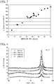
- FIG. 3 shows an example of the relationship between the deposition rate and the critical current Ic.
- the vertical axis of FIG. 3 shows the critical current obtained per unit film-formation time (sec) and unit width (cm-w) by taking the product of the critical current density Jc and the deposition rate.
- the higher the deposition rate the greater the film thickness formed in the same film-formation time.
- the critical current value obtained per unit film-formation time increased almost in proportion to the increase in the deposition rate, it is possible to obtain both an increase in the critical current value and an improvement in productivity.
- Table 1 shows the values of the critical current density Jc and the critical current Ic corresponding to the graphs of FIGS. 2 and 3 .
- Table 1 Deposition Rate [nm/sec] Jc [MA/cm 2 ] Ic [A/sec/cm-w] 5 13.1 71.1 14 10.9 154.2 15 9.9 152.1 23 7.8 179.7 31 8.8 273.4 32 8.0 257.8 36 7.2 256.1 37 7.2 265.9 38 7.2 273.6 41 7.0 287.4 42 7.7 322.4 42 7.4 313.8 43 6.8 292.4 46 6.1 280.5 50 6.1 305.0 55 6.5 355.6 60 6.5 388.7 65 6.2 403.0 70 6.0 420.0
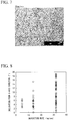
- FIG. 4 shows an example of the dependence of the magnetic field angle (relationship with the direction of the magnetic field) of the critical current value obtained per unit of film formation time.
- the critical current value was measured under the conditions of a temperature of 30K and a magnetic field of 7T.
- a horizontal-axis angle (deg.) was 0° when the angle of the magnetic field was perpendicular to the substrate, and was 90° when the angle of the magnetic field was parallel to the substrate.
- a peak in which the critical current value increased was observed in the vicinity of an angle of 90°, and in a region where the deposition rate was low, a peak due to a linear artificial pinning center rods was observed in the vicinity of an angle of 0°.
- the critical current value tended to be low as a whole.
- the anisotropy decreased in the range of -45° to +45° and the flat dependence of the magnetic field angle was shown.
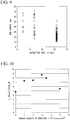
- TEM transmission electron microscope
- FIG. 5 deposition rate of 5 nm/sec
- FIG. 6 deposition rate of 14 nm/sec
- FIG. 7 deposition rate of 32 nm/sec.
- These cross-sectional TEM images are captured images of cross-sections parallel to the thickness direction of the superconducting layer.
- the artificial pinning center rods confirmed by observation of the cross-sectional structure showed a tendency to grow linearly along the c-axis crystal direction of the superconductor when the deposition rate was low.
- the cross sections parallel to the thickness direction of the superconducting layers of Sample Nos. 1 to 6 were observed with a transmission electron microscope (TEM), and the inclination angle and length of the artificial pinning center rods that appeared in the superconducting layer in the region of 140 nm ⁇ 170 nm were measured.
- the inclination angle is an inclination angle of the artificial pinning center rods with respect to the thickness direction of the superconducting layer.
- the length is a length of the artificial pinning center rods along the cross section. In the case where the length direction of the artificial pinning center rods did not follow the cross section, such as when the length was less than the thickness, the case was excluded from the measurement targets of the inclination angle and the length.
- FIG. 8 shows an example of the relationship between the deposition rate and the inclination angle (inclination from the c-axis direction) of the artificial pinning center rods.
- FIG. 9 shows an example of the relationship between the deposition rate and the length of the artificial pinning center rods (rod length).
- Table 2 shows the minimum value, maximum value, average value, and standard deviation of the inclination angle of the artificial pinning center rods measured for each sample.
- Table 3 shows the minimum value, maximum value, average value, and standard deviation of the length of the artificial pinning center rods.
- FIG. 10 shows an example of the relationship between the number density of artificial pinning center rods and the critical current density.
- the number density of artificial pinning center rods is determined by counting the number of artificial pinning center rods within a predetermined range from the plan-view TEM image in the plane perpendicular to the thickness direction of the superconducting layer (ab plane perpendicular to c-axis), and dividing the number by the area corresponding to the range.
- FIG. 10 was created by measuring the number density of artificial pinning center rods of a sample in which a superconducting layer was formed at a deposition rate of about 40 nm/sec, and the critical current density at a temperature of 30K and a magnetic field of 2T.
- critical current density Jc was high when the number density was in the range of 1 ⁇ 10 3 to 3.5 ⁇ 10 3 pieces/ ⁇ m 2 .
- Preferred critical current densities Jc include 6.0 MA/cm 2 or more at a temperature of 30K and a magnetic field of 2T.
- a-axis oriented grains were not observed in any of the number density of artificial pinning center rods of 1 ⁇ 10 3 pieces/ ⁇ m 2 , 2 ⁇ 10 3 pieces/ ⁇ m 2 , 3 ⁇ 10 3 pieces/ ⁇ m 2 , or 5 ⁇ 10 3 pieces/ ⁇ m 2 .
- the ratio of a-axis oriented grains can be calculated from the X-ray intensity ratio. As described above, in order to suppress the decrease in the critical current value, it is preferable that no a-axis oriented grains be observed.
Landscapes
- Chemical & Material Sciences (AREA)
- Organic Chemistry (AREA)
- Engineering & Computer Science (AREA)
- Materials Engineering (AREA)
- Manufacturing & Machinery (AREA)
- Inorganic Chemistry (AREA)
- Ceramic Engineering (AREA)
- Chemical Kinetics & Catalysis (AREA)
- Mechanical Engineering (AREA)
- Metallurgy (AREA)
- Structural Engineering (AREA)
- Toxicology (AREA)
- Health & Medical Sciences (AREA)
- Physics & Mathematics (AREA)
- Optics & Photonics (AREA)
- Superconductors And Manufacturing Methods Therefor (AREA)
- Inorganic Compounds Of Heavy Metals (AREA)
Applications Claiming Priority (2)
| Application Number | Priority Date | Filing Date | Title |
|---|---|---|---|
| JP2018248245 | 2018-12-28 | ||
| PCT/JP2019/048094 WO2020137490A1 (ja) | 2018-12-28 | 2019-12-09 | 酸化物超電導線材及びその製造方法 |
Publications (2)
| Publication Number | Publication Date |
|---|---|
| EP3904292A1 true EP3904292A1 (de) | 2021-11-03 |
| EP3904292A4 EP3904292A4 (de) | 2022-09-21 |
Family
ID=71125850
Family Applications (1)
| Application Number | Title | Priority Date | Filing Date |
|---|---|---|---|
| EP19902603.0A Withdrawn EP3904292A4 (de) | 2018-12-28 | 2019-12-09 | Supraleitender oxiddraht und verfahren zur herstellung davon |
Country Status (6)
| Country | Link |
|---|---|
| US (1) | US11267722B2 (de) |
| EP (1) | EP3904292A4 (de) |
| JP (1) | JP6788152B1 (de) |
| CN (1) | CN112469668A (de) |
| RU (1) | RU2753187C1 (de) |
| WO (1) | WO2020137490A1 (de) |
Families Citing this family (3)
| Publication number | Priority date | Publication date | Assignee | Title |
|---|---|---|---|---|
| JP6919042B1 (ja) * | 2020-09-25 | 2021-08-11 | 株式会社フジクラ | 酸化物超電導線材 |
| RU2761855C1 (ru) * | 2021-07-21 | 2021-12-13 | Общество с ограниченной ответственностью "С-Инновации" | Гибкий высокотемпературный сверхпроводник и способ его получения |
| CN121148812B (zh) * | 2025-11-17 | 2026-04-28 | 甚磁科技(上海)有限公司 | 一种临界电流密度非均匀分布的高温超导带材及其制备方法 |
Family Cites Families (9)
| Publication number | Priority date | Publication date | Assignee | Title |
|---|---|---|---|---|
| JPS54158254A (en) | 1978-06-02 | 1979-12-13 | Mitsutoyo Seisakusho | Contact probe |
| JP2005056754A (ja) * | 2003-08-06 | 2005-03-03 | Sumitomo Electric Ind Ltd | 超電導線材およびその製造方法 |
| US8034745B2 (en) * | 2005-08-01 | 2011-10-11 | Amit Goyal | High performance devices enabled by epitaxial, preferentially oriented, nanodots and/or nanorods |
| ES2302637B1 (es) * | 2006-12-14 | 2009-06-05 | Consejo Superior Investig. Cientificas | Material superconductor nanoestructurado tipo reba2cu3o7(re=tierra rara o ytrio) con una elevada densidad de centros de anclaje de vortices y su metodo de preparacion. |
| EP2728589A4 (de) * | 2011-06-30 | 2015-04-15 | Int Superconductivity Tech | Supraleitender re-123-draht und verfahren zu seiner herstellung |
| CN104054143B (zh) * | 2012-01-17 | 2016-08-31 | 株式会社瑞蓝 | 超导线及其形成方法 |
| WO2014103995A1 (ja) | 2012-12-28 | 2014-07-03 | 公益財団法人国際超電導産業技術研究センター | Re123系超電導線材およびその製造方法 |
| JP6374365B2 (ja) * | 2015-09-16 | 2018-08-15 | 株式会社東芝 | 酸化物超電導体、およびその製造方法 |
| US20190318849A1 (en) | 2016-06-16 | 2019-10-17 | Fujikura Ltd. | Oxide superconducting wire and method for manufacturing same |
-
2019
- 2019-12-09 RU RU2021103698A patent/RU2753187C1/ru active
- 2019-12-09 CN CN201980049207.9A patent/CN112469668A/zh active Pending
- 2019-12-09 WO PCT/JP2019/048094 patent/WO2020137490A1/ja not_active Ceased
- 2019-12-09 US US17/268,334 patent/US11267722B2/en active Active
- 2019-12-09 EP EP19902603.0A patent/EP3904292A4/de not_active Withdrawn
- 2019-12-09 JP JP2020539102A patent/JP6788152B1/ja active Active
Also Published As
| Publication number | Publication date |
|---|---|
| US20210323834A1 (en) | 2021-10-21 |
| EP3904292A4 (de) | 2022-09-21 |
| JPWO2020137490A1 (ja) | 2021-02-18 |
| US11267722B2 (en) | 2022-03-08 |
| RU2753187C1 (ru) | 2021-08-12 |
| CN112469668A (zh) | 2021-03-09 |
| WO2020137490A1 (ja) | 2020-07-02 |
| JP6788152B1 (ja) | 2020-11-18 |
Similar Documents
| Publication | Publication Date | Title |
|---|---|---|
| RU2414769C2 (ru) | Сверхпроводящий провод | |
| WO2001015245A1 (en) | Surface control alloy substrates and methods of manufacture therefor | |
| EP1388899A2 (de) | Oxidsupraleiterdraht | |
| CN103620702B (zh) | Re123系超导线材及其制造方法 | |
| EP3904292A1 (de) | Supraleitender oxiddraht und verfahren zur herstellung davon | |
| EP1973122A1 (de) | Seltenerdhaltiger bandförmiger oxidsupraleiter | |
| US8772201B2 (en) | Oxide superconducting conductor and method of manufacturing the same | |
| EP2562769A1 (de) | Oxidsupraleiter und herstellungsverfahren dafür | |
| US20110034338A1 (en) | CRITICAL CURRENT DENSITY ENHANCEMENT VIA INCORPORATION OF NANOSCALE Ba2(Y,RE)TaO6 IN REBCO FILMS | |
| EP1990810A1 (de) | Verfahren zur herstellung von supraleitendem dünnfilmmaterial, supraleitende einrichtung und supraleitendes dünnfilmmaterial | |
| JP5415824B2 (ja) | 被覆された導体のための、形状を変化させた基板の製造方法及び上記基板を使用する被覆された導体 | |
| US20130137580A1 (en) | Substrate for superconducting thin film, superconducting thin film, and method of producing superconducting thin film | |
| JP5736522B2 (ja) | Re123系超電導線材およびその製造方法 | |
| JP2011249162A (ja) | 超電導線材の製造方法 | |
| JP2020135988A (ja) | 酸化物超電導線材及びその製造方法 | |
| Ko et al. | High $ J_ {\rm c} $${\hbox {GdBa}} _ {2}{\hbox {Cu}} _ {3}{\hbox {O}} _ {7-\delta} $ Coated Conductors on ${\hbox {CeO}} _ {2} $-Buffered IBAD MgO Template Fabricated by Pulsed Laser Deposition |
Legal Events
| Date | Code | Title | Description |
|---|---|---|---|
| STAA | Information on the status of an ep patent application or granted ep patent |
Free format text: STATUS: THE INTERNATIONAL PUBLICATION HAS BEEN MADE |
|
| PUAI | Public reference made under article 153(3) epc to a published international application that has entered the european phase |
Free format text: ORIGINAL CODE: 0009012 |
|
| STAA | Information on the status of an ep patent application or granted ep patent |
Free format text: STATUS: REQUEST FOR EXAMINATION WAS MADE |
|
| 17P | Request for examination filed |
Effective date: 20210210 |
|
| AK | Designated contracting states |
Kind code of ref document: A1 Designated state(s): AL AT BE BG CH CY CZ DE DK EE ES FI FR GB GR HR HU IE IS IT LI LT LU LV MC MK MT NL NO PL PT RO RS SE SI SK SM TR |
|
| DAV | Request for validation of the european patent (deleted) | ||
| DAX | Request for extension of the european patent (deleted) | ||
| REG | Reference to a national code |
Ref country code: DE Ref legal event code: R079 Free format text: PREVIOUS MAIN CLASS: C01G0001000000 Ipc: C23C0014080000 |
|
| A4 | Supplementary search report drawn up and despatched |
Effective date: 20220822 |
|
| RIC1 | Information provided on ipc code assigned before grant |
Ipc: H01F 6/06 20060101ALN20220817BHEP Ipc: H01B 12/06 20060101ALN20220817BHEP Ipc: H01B 13/00 20060101ALI20220817BHEP Ipc: H01B 1/08 20060101ALI20220817BHEP Ipc: C04B 35/45 20060101ALI20220817BHEP Ipc: C01G 27/00 20060101ALI20220817BHEP Ipc: C01G 25/00 20060101ALI20220817BHEP Ipc: C01G 19/00 20060101ALI20220817BHEP Ipc: C01G 3/00 20060101ALI20220817BHEP Ipc: H01L 39/24 20060101ALI20220817BHEP Ipc: H01L 39/14 20060101ALI20220817BHEP Ipc: C23C 14/28 20060101ALI20220817BHEP Ipc: C23C 14/08 20060101AFI20220817BHEP |
|
| STAA | Information on the status of an ep patent application or granted ep patent |
Free format text: STATUS: EXAMINATION IS IN PROGRESS |
|
| 17Q | First examination report despatched |
Effective date: 20230503 |
|
| STAA | Information on the status of an ep patent application or granted ep patent |
Free format text: STATUS: THE APPLICATION HAS BEEN WITHDRAWN |
|
| 18W | Application withdrawn |
Effective date: 20230829 |