EP3907764A1 - Agencement pour une antenne permettant de générer ou de recevoir un rayonnement térahertz, antenne, système térahertz ainsi que procédé de fabrication d'un agencement pour une antenne - Google Patents
Agencement pour une antenne permettant de générer ou de recevoir un rayonnement térahertz, antenne, système térahertz ainsi que procédé de fabrication d'un agencement pour une antenne Download PDFInfo
- Publication number
- EP3907764A1 EP3907764A1 EP20173549.5A EP20173549A EP3907764A1 EP 3907764 A1 EP3907764 A1 EP 3907764A1 EP 20173549 A EP20173549 A EP 20173549A EP 3907764 A1 EP3907764 A1 EP 3907764A1
- Authority
- EP
- European Patent Office
- Prior art keywords
- substrate
- photoactive layer
- antenna
- carrier
- layer
- Prior art date
- Legal status (The legal status is an assumption and is not a legal conclusion. Google has not performed a legal analysis and makes no representation as to the accuracy of the status listed.)
- Withdrawn
Links
Images




Classifications
-
- H—ELECTRICITY
- H10—SEMICONDUCTOR DEVICES; ELECTRIC SOLID-STATE DEVICES NOT OTHERWISE PROVIDED FOR
- H10F—INORGANIC SEMICONDUCTOR DEVICES SENSITIVE TO INFRARED RADIATION, LIGHT, ELECTROMAGNETIC RADIATION OF SHORTER WAVELENGTH OR CORPUSCULAR RADIATION
- H10F30/00—Individual radiation-sensitive semiconductor devices in which radiation controls the flow of current through the devices, e.g. photodetectors
- H10F30/20—Individual radiation-sensitive semiconductor devices in which radiation controls the flow of current through the devices, e.g. photodetectors the devices having potential barriers, e.g. phototransistors
- H10F30/21—Individual radiation-sensitive semiconductor devices in which radiation controls the flow of current through the devices, e.g. photodetectors the devices having potential barriers, e.g. phototransistors the devices being sensitive to infrared, visible or ultraviolet radiation
-
- H—ELECTRICITY
- H01—ELECTRIC ELEMENTS
- H01Q—ANTENNAS, i.e. RADIO AERIALS
- H01Q1/00—Details of, or arrangements associated with, antennas
- H01Q1/12—Supports; Mounting means
- H01Q1/22—Supports; Mounting means by structural association with other equipment or articles
- H01Q1/2283—Supports; Mounting means by structural association with other equipment or articles mounted in or on the surface of a semiconductor substrate as a chip-type antenna or integrated with other components into an IC package
-
- H—ELECTRICITY
- H01—ELECTRIC ELEMENTS
- H01Q—ANTENNAS, i.e. RADIO AERIALS
- H01Q5/00—Arrangements for simultaneous operation of antennas on two or more different wavebands, e.g. dual-band or multi-band arrangements
- H01Q5/20—Arrangements for simultaneous operation of antennas on two or more different wavebands, e.g. dual-band or multi-band arrangements characterised by the operating wavebands
- H01Q5/22—RF wavebands combined with non-RF wavebands, e.g. infrared or optical
-
- H—ELECTRICITY
- H10—SEMICONDUCTOR DEVICES; ELECTRIC SOLID-STATE DEVICES NOT OTHERWISE PROVIDED FOR
- H10F—INORGANIC SEMICONDUCTOR DEVICES SENSITIVE TO INFRARED RADIATION, LIGHT, ELECTROMAGNETIC RADIATION OF SHORTER WAVELENGTH OR CORPUSCULAR RADIATION
- H10F71/00—Manufacture or treatment of devices covered by this subclass
- H10F71/139—Manufacture or treatment of devices covered by this subclass using temporary substrates
-
- H—ELECTRICITY
- H10—SEMICONDUCTOR DEVICES; ELECTRIC SOLID-STATE DEVICES NOT OTHERWISE PROVIDED FOR
- H10F—INORGANIC SEMICONDUCTOR DEVICES SENSITIVE TO INFRARED RADIATION, LIGHT, ELECTROMAGNETIC RADIATION OF SHORTER WAVELENGTH OR CORPUSCULAR RADIATION
- H10F77/00—Constructional details of devices covered by this subclass
- H10F77/10—Semiconductor bodies
- H10F77/12—Active materials
- H10F77/124—Active materials comprising only Group III-V materials, e.g. GaAs
- H10F77/1248—Active materials comprising only Group III-V materials, e.g. GaAs having three or more elements, e.g. GaAlAs, InGaAs or InGaAsP
-
- H—ELECTRICITY
- H10—SEMICONDUCTOR DEVICES; ELECTRIC SOLID-STATE DEVICES NOT OTHERWISE PROVIDED FOR
- H10F—INORGANIC SEMICONDUCTOR DEVICES SENSITIVE TO INFRARED RADIATION, LIGHT, ELECTROMAGNETIC RADIATION OF SHORTER WAVELENGTH OR CORPUSCULAR RADIATION
- H10F77/00—Constructional details of devices covered by this subclass
- H10F77/40—Optical elements or arrangements
- H10F77/407—Optical elements or arrangements indirectly associated with the devices
Definitions
- the present invention relates to an arrangement for an antenna for generating or receiving terahertz radiation, an antenna for generating or receiving terahertz radiation, a terahertz system for generating and coherently detecting terahertz radiation and a method for producing an arrangement for an antenna for generating or receiving terahertz radiation.
- Terahertz radiation is electromagnetic radiation with a frequency of between 0.05 THz and 20 THz, the frequency typically being between 0.1 THz and 10 THz.
- these frequencies are very high, compared to the frequencies typical for photonics, on the other hand, very small, so that the quantum energy of terahertz radiation is still very low. Measuring systems working with terahertz radiation are therefore difficult to implement, which is why terahertz radiation forms the last area of the electromagnetic spectrum that has not yet been developed to a satisfactory extent for practical applications.
- a terahertz system usually comprises a laser light source and two THz antennas, each optically coupled to the laser light source via an optical fiber and activated by light from this laser light source, of which a first serves as a transmitting antenna and a second as a receiving antenna.
- the THz antennas each have a semiconductor chip which is contacted with antenna conductors and which comprises at least one photosensitive active layer with a band edge wavelength that is greater than a wavelength of the laser light source and at least one layer adjoining the active layer with a band edge wavelength that is smaller than the wavelength of the laser light source.
- the antenna conductors are typically integrated on the respective semiconductor chip.
- the laser light source can be used to generate short pulses or to generate beat signals in the THz range by superimposing two laser waves of slightly different wavelengths be trained.
- the wavelength of a laser light source is defined in the present document as the focal point of a wavelength spectrum of the light generated by the laser light source.
- terahertz radiation can now be generated and coherently detected by applying a voltage to the antenna conductors of the transmitting antenna, while the transmitting antenna and the receiving antenna are activated simultaneously or with an adjustable delay with coherent radiation from the laser light source and a current generated in the receiving antenna is measured by means of a sensor connected to the antenna conductors of the receiver antenna.
- a received signal for various delays of a light transit time between the laser light source and the receiving antenna or the transmitting antenna can be detected in this way.
- Terahertz systems of this type are, for example, from the publications DE 10 2007 044 839 A1 and DE 10 2010 049 658 A1 known.
- these terahertz systems can be implemented advantageously compact, robust and flexible.
- the THz antenna 30 of the Fig. 1 comprises a photoactive layer 21 with fast charge carrier recombination time, which was produced by epitaxial growth on an electrically insulating substrate 22.
- a metallic structure 23, 24 is formed as a THz antenna on the photoactive layer, which can be formed, for example, in dipole, bowtie or strip-line geometry.
- the metallic structure 23, 24 has a gap through which a short (fs range) light pulse 11 can be directed onto the photoactive layer 21.
- the antenna 20 of the Fig. 1 is designed as a THz transmitter, for example.
- the THz transmitter 20 a voltage is applied to the metallic structure 23, 24.
- photocarriers are generated in the photoactive layer and are strongly accelerated in the electric field, as a result of which electromagnetic radiation in the THz range (0.1 - 10 THz) is generated.
- the radiation preferably propagates in the semiconductor material of the layer 21 and of the substrate 22.
- the antenna chip or the substrate 22 is attached to the flat surface of a hyper-hemispherical Si lens 25 made of highly pure Si with high THz transparency.
- the THz receiver looks identical. But no voltage is applied here. Instead, the photocurrent caused by received THz radiation and excited photo charge carriers is measured in the THz receiver. A photocurrent only flows if - at the same time - a voltage is applied by the received THz radiation and the photoconductivity is effected by the light pulse.
- a delay line is therefore installed in one of the beam paths, through which the temporal position of the received THz radiation and the scanning fs light pulse can be varied. A "coherent" detection is thus effected, and the amplitude and phase of the THz wave are scanned in a pump-probe method with high sensitivity and high speed potential.
- the first THz systems used an excitation wavelength at 800 nm, as powerful pulse lasers with fs-small pulse width and photoconductors made from "low temperature" grown LT-GaAs on a GaAs substrate with a very fast recombination time were available.
- New systems often use excitation wavelengths at 1300 nm and at 1550 nm, since many components from developments for optical telecommunications technology are available here.
- Femtosecond fiber lasers at 1550 nm are now inexpensive and maintenance-free, and glass fibers allow flexible connections from the laser to movable transmission and detection heads. This offers considerable advantages for the industrial use of THz sensors.
- GaAs does not absorb at 1550 nm, fast photoconductors first had to be developed for this wavelength range.
- InGaAs, InGaAsP, InAlAs, InGaAlAsP and InGaAlAs layers which are each grown on an InP substrate in an epitaxially lattice-adapted manner.
- a typical thickness of the photoconductor layers is in the range 1-2 ⁇ m, which roughly corresponds to the penetration depth (1 / e) of the exciting light. Thicker layers require more effort for epitaxial growth. However, hardly any photo charge carriers are generated any more. On the other hand, the background dark current (noise) increases unfavorably. In addition, long distances from the excitation location deep in the layer to surface contacts have an unfavorable influence on the time behavior (bandwidth of detection).
- the stimulating optical radiation is not completely absorbed in the advantageously thin layers. With 800 nm systems this is not a problem, because the GaAs substrate also absorbs here, and with a typical substrate thickness of 300 - 500 ⁇ m the stimulating optical radiation is completely removed from the system.
- the InP substrate is typically transparent for wavelengths above 1000 nm. Residual light behind the photoactive layer (i.e. behind the photoconductor), which was not absorbed by the photoactive layer, is therefore not absorbed in the downstream substrate, but remains in the system and can impair its function. It is particularly critical if residual light pulses activate the transmitting or receiving antenna with the wrong timing. In this way, the laser pulse stimulating the transmitting antenna can also reach the receiving antenna via the THz imaging optics. In the prior art, light filters in the THz beam path are used to block this path. What cannot be achieved with these external filters, however, is the blocking of interference pulses that arise from internal reflections at interfaces within the THz antennas.
- Such internal optical reflections are indicated by the dashed lines in FIG Fig. 2 indicated, the Fig. 2 a similar structure as the Fig. 1 shows. If these laser pulses excite the conductor layer a second time with an unfavorable time delay and thus generate “echo” -THz pulses 27 there, then this can considerably impair the function of a THz sensor system. Measurements of a system in the prior art show these interference pulses very clearly, see THz echo pulses 27 of FIG Fig. 3 . It would therefore be advantageous if these THz echo pulses 27 caused by optical reflections can be avoided or at least reduced, since echo pulses can significantly interfere with even the smallest amplitude measurements.
- the disturbance of the echo pulse is estimated on the basis of the spatial extent of the optical pulse and at nearby interfaces.
- n 3
- a spatially 10 ⁇ m larger pulse stimulates the photoconductor. Reflections at the photoconductor interface or close to it are not perceived as a separate echo, but become part of a somewhat wider excitation pulse.
- a free photoconductor layer would therefore not generate any echoes at the interfaces despite large jumps in the refractive index. However, such a layer would not be sufficiently stable mechanically.
- the disturbance of the echo pulse can be estimated as follows. Reflections at more distant interfaces lead to echo pulses typically far outside the measurement window. So have the reflection on the outside of a Si lens (see. Lens 25 of the Fig. 1 ) against air - because of the high refractive index jump ⁇ n of about 2.5 (refractive index of Si: 3.478 at a wavelength of 1550 nm, refractive index of air: approx. 1 at a wavelength of 1550 nm) - a very high amplitude.
- the distance between the photoconductor layer and the outside of the Si lens is quite large at 7.35 mm, with a thickness of the InP substrate of about 350 ⁇ m and a thickness of the Si lens of about 7 mm being assumed. Since the echo pulse traverses this path twice, the additional running distance compared to the original pulse is about 14.7 mm. If the refractive index of approx. 3.4 is also taken into account, there is even an additional optical path of approx. 50 mm and thus a delay of the echo pulse of approx. 150 ps. This means that these echo pulses lie outside the typical measurement window and generally do not interfere with the measurements.
- this areally flush contact is difficult to achieve, in particular because of the limited planarity of the brittle InP substrate. If, as a consequence, an air gap forms between InP and Si in some areas, then significantly higher reflections can be expected at the semiconductor-air interfaces.
- the width of the air gap relative to the wavelength also plays a role here.
- the relatively slowly decaying wave protrudes through a sub- ⁇ m gap into the second semiconductor material and spreads there, so that a high reflection does not yet develop here can.
- the stimulating laser pulse with a wavelength of e.g. 1.5 ⁇ m the first resonator mode of the highest reflection forms at a slit width of 0.75 ⁇ m (half a wavelength), and the increase in reflection therefore starts at smaller slit widths.
- Small sub- ⁇ m air gaps therefore have hardly any effect on THz waves because of the different wavelengths by orders of magnitude, while the optical excitation pulse experiences a high level of reflection.
- the pulses reflected on the front and back of the layer are around (with an assumed refractive index for the sample of 1.5) also a few ps apart. If one takes into account the multi-layer structure of the sample, the width of the THz pulses, and the low amplitude of the reflection at the inner lacquer interfaces, it becomes clear that echo pulses at this time significantly impair the measurement accuracy.
- the reflections between the InP substrate and the Si lens are actually the critical reflections, as measurements when using THz antennas in a time domain system show (cf. Fig. 3 ).
- Pre- and post-pulses are observed at a distance of approx. 7 ps from the main pulse. As described above, these 7 ps correspond exactly to the time delay of echo pulses due to reflection of the laser pulse at the interface between the InP substrate and the Si lens. Due to fluctuations in the thickness of the InP substrate (nominally 350 ⁇ m), the timing of one pulse varies slightly when different THz transmitter chips are compared.
- the echo pulses on the other side of the time axis are caused by the reflections of the fs laser in the THz receiver.
- the receiver is the same in all measurements, which is why the associated echo pulses are well superimposed.
- these echo pulses can therefore be calculated out in a fixed measuring system. However, it becomes critical when a weak measurement signal is close to one of the echo pulses. This should be explained using an important application example.
- THz radiation 0.1 THz to 30 THz
- dielectric materials such as plastics, lacquers and paper that are opaque to visible light.
- a THz pulse 12 is directed onto a painted metal surface 33.
- the lacquer layers 32 typically rust protection - filling - colored lacquer - clear lacquer
- the reflected THz pulses 34 are now passed to the receiving antenna 31 and there the time offset of the reflected THz pulses is measured with the scanning laser pulse. If the refractive indices of the layers 32 are known, the individual thicknesses in the layer package can now be determined.
- the refractive indices of the lacquers are often in the range from 1.5 to 1.6 for THz radiation.
- this object is achieved by an arrangement, an antenna, a terahertz system and a method according to the independent claims. Developments are the subject of the dependent claims and the description below.
- the substrate and the carrier are made of the same material.
- the arrangement furthermore has a first adhesion-promoting layer, the first adhesion-promoting layer being arranged between the photoactive layer and the substrate and connecting the two to one another over a large area.
- the first adhesion-promoting layer has a layer thickness of at most 5 ⁇ m.
- the substrate and the carrier are made of the same material, they have the same refractive index. As a result, there is no jump in the refractive index when the materials transition. As a result, reflections at the boundary surfaces of the materials and thus the above-mentioned optical reflections or the optical echo pulses can be reduced considerably.
- the first adhesion-promoting layer enables a surface flush contact between the photoactive layer and the substrate. In this way, air gaps between the photoactive layer and the substrate can in particular be prevented or reduced. Due to the small layer thickness of the adhesion-promoting layer, interfaces can be brought close to the photoactive layer, so that pulses reflected at the interface between substrate and adhesion-promoting layer lie within the pulse width of the original optical pulses. The reflected optical pulses can thereby merge with the original pulse, whereby the formation of separate echo pulses can be avoided.
- Materials or components should be referred to as transparent in the context of the present document if they are permeable to at least 90% and / or at least 95% and / or 99% of the incident radiation in the electromagnetic spectral range of interest.
- the substrate can have a thickness which is at least 10 times or at least 100 times greater than the layer thickness of the photoactive layer. It can be provided that the substrate has a substrate thickness of at most 1 mm, preferably at most 0.5 mm and / or at least 0.2 mm, in particular at least 0.3 mm. Such substrate thicknesses are typical for semiconductor wafers or wafers.
- the substrate can thus be made from a semiconductor wafer, preferably a wafer or a semiconductor chip.
- the photoactive layer attached to the wafer can then be subjected to a typical wafer processing and a large number of structures can thus be processed in parallel.
- a side of the substrate facing away from the photoactive layer is preferably directly adjacent to the carrier. This can also reduce annoying reflections.
- the carrier has a carrier thickness of at least 3 mm, preferably at least 5 mm, in particular at least 7 mm.
- the substrate thickness is thus usually smaller than the carrier thickness.
- the carrier thickness can, for example, be at least five times as great as the substrate thickness. Due to the relatively large carrier thickness compared to the layer thickness and the substrate thickness, the optical transit times of the optical radiation in the carrier can be relatively long, as a result of which the optical reflections can be shifted in time. In this way, unavoidable reflective interfaces at a distance from the photoactive layer can be shifted outside of a measurement window of interest for a measurement by increasing the thickness of the adjacent carrier, so that the measurement is no longer impaired.
- thicknesses or layer thicknesses are preferably measured perpendicular to layer planes and / or perpendicular to planar surfaces. Typically, all thicknesses and layer thicknesses are measured along the same direction.
- a side of the photoactive layer facing away from the substrate is at least partially free of coating and in particular is exposed to the ambient air.
- the side of the photoactive layer facing away from the substrate may have InP residues in some areas.
- the optical radiation in the sense of the present document is understood as the electromagnetic radiation which is required to excite the photoactive layer, so that electron-hole pairs are generated in the photoactive layer.
- the excitation energy of the optical radiation depends on a band gap, i.e. a distance between a valence band and a conduction band, of the photoactive material used.
- the photoactive material of the photoactive layer can be selected in such a way that the band gap is matched to a specific excitation energy. If the band gap is temperature-dependent, its values, defined in the usual way, are always meant here at operating temperature, typically between 10 ° C and 50 ° C, preferably between 15 ° C and 25 ° C.
- the photoactive layer will have a band gap which corresponds to an excitation wavelength of at least 1200 nm, preferably at least 1250 and / or at most 1700 nm, preferably at most 1650 nm.
- the photoactive layer can for example be produced at least predominantly from a semiconductor material such as InGaAs, InAlAs, InGaAsP, InGaAlAs, InGaAlAsP and / or GaAlAs, or comprise a combination of several semiconductors.
- the semiconductor used is usually doped with a transition metal, in particular Fe, Rh or Ru.
- a concentration of the transition metal in the photoactive layer can be at least 10 18 cm -3 , preferably at least 10 19 cm -3 .
- the photoactive layer is preferably formed from a single layer of the photoactive material.
- the photoactive layer can comprise a plurality of partial layers.
- at least one active layer and an adjacent layer can be provided.
- the active layer or each of the active layers can each be embedded between two adjacent layers.
- the adjacent layers serve as recombination layers.
- the photoactive layer has a periodic layer structure with a multiplicity of alternately arranged active layers and recombination layers n; where z. B. 100 or more active layers can be provided.
- the effect of remaining echo pulses can be further minimized or reduced by restricting the expansion of the photoactive layer to the absolutely necessary area.
- the photoactive layer can have a base area of at most 1 mm 2 , preferably at most 0.1 mm 2 , preferably at most 0.01 mm 2 .
- a perpendicular projection of the photoactive layer onto the substrate can have an area of at most 1 mm 2 , preferably at most 0.1 mm 2 , preferably at most 0.01 mm 2 .
- the aforementioned projection perpendicular to the substrate is a parallel projection, ie the projection rays emanating from the photoactive layer, which are referred to as projection lines, are parallel to one another.
- the photoactive layer can have a lateral extent measured parallel to the substrate and / or a diameter of at most 1 mm, preferably at most 0.1 mm.
- the photoactive layer can in particular be in the form of a mesa structure.
- the substrate can be designed, for example, as a plane-parallel plate.
- the carrier can be designed as a plane-parallel body or as a wedge-shaped body.
- the substrate can be directly adjacent to the carrier, i.e. without an adhesive bond or layer in between.
- a second adhesion-promoting layer is provided, which is arranged between the substrate and the carrier and connects the two to one another over a large area.
- the first adhesion-promoting layer and the second adhesion-promoting layer can consist of the same material or comprise different materials. Different materials can be used for the respective adhesion-promoting layers. On the one hand, the material should connect the components to be connected to one another in a flat and flush manner. On the other hand, the material should be transparent to the THz radiation and / or the optical radiation.
- the first is adhesion promoting Layer and / or the second adhesion-promoting layer is an adhesive layer, for example a layer of benzocyclobutene (BCB). Other suitable materials are also conceivable.
- the substrate is designed as a silicon wafer.
- the carrier can be designed as a silicon body. Silicon wafers and silicon bodies are available with high surface planarity.
- thin Si wafers (0.2 mm - 1 mm) are usually elastic and bendable and adapt well to the adjoining silicon body, i.e. to the carrier.
- van der Waals forces / cohesion can create seamless Si-Si connections between the substrate in the form of a Si wafer and the carrier in the form of a Si body. In this way, air gaps between the carrier and the substrate, and thus refractive index jumps, can advantageously be avoided.
- the arrangement can also have a lens for the terahertz radiation.
- convex lenses preferably plano-convex lenses, are used.
- a hemispheric lens or a hyperhemispheric lens is used.
- the lens is attached to the carrier.
- the lens can be adjacent to the wearer.
- a third adhesion-promoting layer can also be provided between the carrier and the lens, which connects the two with one another over a large area.
- the lens can form the carrier.
- the substrate is attached directly to the lens without an additional carrier being present.
- the lens is made from the same material as the substrate and / or the carrier.
- the lens can also be made of a polymer material such as polymethylpentene (also called TPX or PMP).
- a lens thickness, usually measured at a thickest point on the lens, can be at least 2 mm, preferably at least 3 mm.
- the lens thickness and the carrier thickness can be the same.
- the substrate and / or the carrier and / or the lens are usually made of an electrically insulating material.
- the substrate and / or the carrier and / or the lens are usually transparent to the terahertz radiation generated. Furthermore, the lens is usually also transparent to the optical radiation.
- an antenna for generating or receiving terahertz radiation comprises the arrangement of the type described above. Furthermore, the antenna has an antenna conductor with a first partial structure and a second partial structure. The first partial structure and the second partial structure are spaced apart from one another by a gap and contact the photoactive layer.
- the substructures can contact the photoactive layer both electrically and mechanically.
- the antenna conductor is usually made of one metal and in this case can have two metal structures. In particular, the antenna conductor can be formed by vapor-deposited or sputtered metal.
- the geometry of the substructures creates e.g. dipole, bow-tie or so-called strip-line antennas.
- the photoactive layer can be in contact with the antenna conductor on a surface or on lateral end faces.
- the antenna conductor is arranged on a side of the photoactive layer facing away from or facing the substrate.
- the first partial structure and the second partial structure can be arranged next to the photoactive layer on the substrate. In this case, the photoactive layer can be arranged between the two structures.
- a terahertz system for generating and coherently detecting terahertz radiation.
- the terahertz system comprises a laser light source and two THz antennas, each optically coupled to the laser light source and activated by optical radiation from this laser light source, of which a first serves as a transmitting antenna and a second as a receiving antenna.
- the transmitting antenna and / or the receiving antenna each comprise an antenna of the type described above Art.
- the light from the laser light source preferably has a wavelength of at least 1200 nm, in particular at least 1250 nm and / or at most 1700 nm, in particular at most 1680 nm.
- a pulse laser is used as the laser light source.
- CW laser continuous wave laser
- a femtosecond pulse laser with a wavelength between 1200 nm and 1700 nm can be used.
- Femtosecond pulses have a duration of less than a picosecond, e.g. between 10 fs and 990 fs.
- the laser light source can be designed as an optical beat source.
- the laser light source can be a dual mode laser or a system of two lasers and be set up to generate a beat signal of two laser waves, with a beat frequency of this beat signal being at least 0.05 THz and typically between 0.05 THz and 20 THz, preferably between 0 , 1 THz and 10 THz so that the terahertz radiation can be generated with the appropriate frequency and wavelength.
- a lens arrangement is preferably provided for focusing the laser light on the photoactive layer. Since the laser light or the optical radiation is usually not completely absorbed by the photoactive layer, a remaining part of the light passes through the photoactive layer and downstream layers (substrate, adhesion-promoting layer, carrier and / or THz lens). An optical echo pulse reflected at a certain distance typically strikes the photoactive layer in a divergent manner and can there again generate photo charge carriers over a large area. Even at a certain distance from the substructures of the antenna conductor, these photo charge carriers can still activate the antenna conductor, whereby THz echo pulses are generated.
- the photoactive layer can be designed as a mesa structure, for example.
- the substructures can then be designed as side contacts.
- the photoelectric effect does not take place outside the mesa, and so a large part of the optical echo pulses remains ineffective with regard to the excitation of the photoactive layer.
- a preferred maximum lateral extent or areal extent of the photoactive layer reference is made to the dimensions mentioned above.
- the photoactive layer can be activated by optical radiation in the range from 1200 nm to 1700 nm.
- the substrate and the carrier are made of the same material.
- the substrate and the carrier are also transparent to the optical radiation.
- the photoactive layer can in particular be grown on the auxiliary substrate made of InP in an epitaxially lattice-adapted manner.
- Suitable materials for the photoactive layer with the required band gap can include InGaAs, InAIAs, InGaAsP, InGaAlAs, InGaAlAsP and / or GaAlAs.
- the InP material is only used as an auxiliary substrate for growing the photoactive layer.
- the auxiliary substrate made of InP is removed.
- the auxiliary substrate is preferably removed by chemical etching.
- the auxiliary substrate can be removed by mechanical etching.
- the auxiliary substrate is preferably completely removed.
- the photoactive layer produced on the InP auxiliary substrate alone is generally not sufficiently mechanically stable, since the photoactive layer often has a layer thickness of at most a few micrometers. For this reason, the photoactive layer is connected to the substrate before the InP auxiliary substrate is removed, which is thus provided for stabilizing the photoactive layer. Before the auxiliary substrate is removed, the substrate and the auxiliary substrate are usually located on opposite sides of the photoactive layer.
- the photoactive layer is grown by means of molecular beam epitaxy at a temperature of 200 ° C. to 450 ° C., preferably 400 ° C.
- the photoactive layer is grown epitaxially and with a transition metal such as Fe, Rh, or Ru doped, preferably in concentrations above 10 18 cm -3 .
- the step of applying the antenna conductor to the photoactive layer can take place before connecting the photoactive layer to the substrate or after removing the auxiliary substrate.
- a lateral expansion of the photoactive layer can be reduced. This can be done wet-chemically and / or by dry etching processes, for example.
- surface passivation can be provided on the photoactive layer.
- the surface passivation can comprise silicon nitride and / or silicon oxide, for example.
- the substrate Before it is attached to the carrier, the substrate can still be present as an unprocessed wafer on which at least one structure is arranged.
- at least one structure comprising the photoactive layer, the first adhesion-promoting layer and / or the antenna conductor can be attached to the substrate.
- a large number of separate structures for example at least 5, at least 10, at least 50 or even at least 100 structures, are arranged on the substrate.
- the active layer on the substrate can be processed using established technologies in semiconductor production for the parallel configuration of a large number of different structures.
- the different, processed structures can then be isolated or separated from one another.
- the substrate wafer can be divided into individual chips. The method can thus be completed by separating the structures processed on the substrate and fastening the substrate with the processed structure on the carrier to form the above-mentioned arrangement.
- the method is particularly suitable for producing the aforementioned arrangement and the aforementioned antenna.
- Features mentioned in relation to the arrangement and the antenna can also be claimed for the method and vice versa.
- the terahertz system 20 shown has a laser light source 15, a transmitting antenna 16 and a receiving antenna 17.
- the transmitting antenna 16 and the receiving antenna 17 are each a THz antenna that can be activated by light from the laser light source 15.
- a beam splitter 28 is connected behind an output of the laser light source 15, the transmitting antenna 16 and the receiving antenna 17 each being connected by an optical fiber 18 to one of two outputs of the beam splitter 28.
- the laser light source 15 is a pulse laser, the wavelength of the laser light source 15 being between 1200 nm and 1700 nm and preferably 1300 nm or 1550 nm.
- a controllable optical delay circuit 19 can be arranged at an input or in a course of one of the optical fibers 18, with which a relative timing of optical control signals for activating the two THz antennas 16, 17 can be shifted.
- the delay circuit 19 can have, for example, a delay line to which a variable electrical field can be applied.
- a sample 29, which is arranged between the transmitting antenna 16 and the receiving antenna 17 and can be examined with the terahertz system 20, is also shown.
- the pulse laser forming the laser light source 15 can be a fiber pulse laser, e.g. with erbium doping, or a semiconductor pulse laser, e.g. based on an InGaAsP / InP material system.
- the Figures 6 to 10 schematically show THz antennas according to embodiments of the present invention. For the sake of clarity, only THz transmission antennas 16 are shown here. However, it is clear that those in the Figures 6-10 THz transmitting antennas shown can also be used as THz receiving antennas.
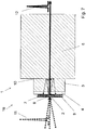
- the Fig. 6 shows schematically an arrangement 1 which is a component of the antenna 16 for generating terahertz radiation 12.
- the arrangement 1 comprises a photoactive layer 2, a substrate 3, a first adhesion-promoting layer 4 and a carrier 5.
- the photoactive layer 2 can be activated by optical radiation 11 from the laser 15 in the range from 1200 nm to 1700 nm and thus has a corresponding band gap.
- Suitable semiconductors for the photoactive layer 2 would be, for example, InGaAs, InAlAs, InGaAsP, InGaAlAs, InGaAlAsP or GaAlAs.
- the semiconductor used for the photoactive layer 2 is usually doped with a transition metal such as Fe, Rh or Ru, in a concentration of at least 10 18 cm -3 , preferably at least 10 19 cm -3. Layer thicknesses of the photoactive layer 2 of at most 10 ⁇ m and at least 0.5 ⁇ m are advantageous for generating THz radiation.
- the total layer thickness can be 1 ⁇ m to 2 ⁇ m.
- the photoactive layer 2 preferably consists of a single layer of the photoactive material.
- the photoactive layer 2 can alternatively comprise a plurality of partial layers. For example, at least one active layer and an adjacent layer can be provided.
- the photoactive layer 2 is attached to the substrate 3.
- the first adhesion-promoting layer 4 applied over a large area is used for the fastening.
- the first adhesion-promoting layer 4 is thus arranged between the photoactive layer 2 and the substrate 3 and connects both of them flat and flush with one another.
- the adhesion-promoting layer 4 allows air gaps between the substrate 3 and the photoactive layer 2 to be largely avoided.
- a layer thickness of the adhesion-promoting layer 4 should be at most 5 ⁇ m. Layer thicknesses in the range 0.5 ⁇ m to 2 ⁇ m would be conceivable.
- a suitable material for the adhesive layer 4, which sometimes also Adhesive layer is called, for example, BCB (benzocyclobutene), which is often used in the prior art for what is known as wafer bonding.
- the substrate 3 consists of a material that is transparent to the laser radiation 11 and the THz radiation 12, preferably silicon.
- the substrate 3 is also electrically insulating.
- the substrate 3 ensures mechanical stability of the photoactive layer 2, in particular during the production of the arrangement 1 (cf. the production method below).
- the substrate 3 is usually designed as a plane-parallel plate.
- the substrate 3 can advantageously be produced from a chip of a commercially available silicon wafer. This allows the use of established technologies of wafer processing and the parallel production of a large number of structures on one substrate.
- a first side of the substrate 3 facing the photoactive layer 2 is thus a planar surface.
- the substrate is attached to the carrier 5.
- the substrate 3 is thus arranged between the photoactive layer 2 and the carrier 5.
- a side of the substrate 3 facing the carrier 5 is preferably also designed as a flat surface.
- the substrate 3 preferably has a substrate thickness, measured perpendicular to a substrate plane from the first side to the second side of the substrate 3, which is substantially greater than the layer thickness of the photoactive layer 2.
- the substrate 3 can, for example, have a substrate thickness of at most 1 mm, substrate thicknesses of at least 0.2 mm being common. In the exemplary embodiment shown, the substrate 3 has a constant substrate thickness in the range from 300 ⁇ m to 500 ⁇ m.
- the carrier 5 is made of the same material as the substrate 3, but has a much greater thickness.
- the carrier 5 is designed as a plane-parallel silicon body or silicon block.
- a first side of the carrier 5 facing the substrate 3 is therefore a planar surface.
- a second side of the carrier 5, which faces away from the substrate 3, is designed as a flat surface.
- the THz radiation 12 generated in the antenna 16 leaves the carrier 5 via the first side of the carrier 5 facing away from the substrate 3.
- the carrier 5 preferably has a carrier thickness measured from the first side to the second side of the carrier 5, which is significantly greater than the substrate thickness and the thickness of the photoactive layer 2.
- optical reflections at the interface between carrier 5 and air, ie on the second side of carrier 5, can be delayed in time so that they lie outside the measurement window of interest.
- Exemplary carrier thicknesses are at least 5 mm, preferably at least 8 mm. Because the carrier 5 and the substrate 3 are made of the same material, reflections of the optical radiation 11 at the interface between the substrate 3 and the carrier 5 are greatly suppressed.
- the carrier 5 and the substrate 3 are connected flush and their sides lie flat against one another, for example via a press contact.
- the carrier 5 can thus directly adjoin the substrate 3.
- a second adhesion-promoting layer (not shown) can also be provided between the substrate 3 and the carrier 5, which connects the substrate 3 and the carrier 5 to one another in a planar and flush manner.
- the second adhesion-promoting layer can consist of a polymer material such as BCB.
- an antenna conductor 6 which comprises a first partial structure 7 and a second partial structure 8.
- the first partial structure 7 and the second partial structure 8 are spaced apart from one another by a gap 9.
- the photoactive layer 2 is free of coating in the area of the mentioned gap 9 and is exposed there to the ambient air.
- the optical radiation 11 of the laser 15 enters the photoactive layer 2 through the gap 9.
- Both substructures 7, 8 contact the photoactive layer 2 both electrically and mechanically.
- the substructures 7, 8 are generally designed as metal structures, wherein they are formed by vapor deposition or sputtering of metal on the photoactive layer 2. In the embodiment of Fig. 6 the substructures 7, 8 are arranged on a side of the photoactive layer 2 facing away from the substrate 3.
- the one in the Fig. 7 THz antenna 16 shown differs from that in FIG Fig. 6 THz antenna shown in that the substructures 7, 8 of the antenna conductor 6 are arranged laterally next to the photoactive layer 2.
- the photoactive layer 2 is thus located centrally between the substructures 7, 8.
- the photoactive layer 2 is located within the gap 9 and fills it completely off.
- the photoactive layer 2 in the embodiment of FIG Fig. 7 designed as a mesa structure with dimensions measured perpendicular to the layer thickness of at most 100 ⁇ m by 100 ⁇ m.
- the mesa structure thus has a base area of at most 0.01 mm 2 .
- FIG Fig. 7 Apart from the arrangement of the substructures 7, 8 relative to the photoactive layer 2 and the implementation of the photoactive layer 2 as a mesa structure, the structure shown in FIG Fig. 7 The antenna 16 shown has the same properties as the antenna of FIG Fig. 6 .
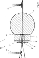
- an antenna 16 is shown, which in addition to the antenna 16 of the Fig. 6 has a lens 13 for THz radiation 12.
- the lens 13 couples the THz radiation 12 out of the antenna 16 and in the exemplary embodiment is shown in FIG Fig. 8 designed as a plano-convex lens, in particular a hemispherical lens or a hyperhemispherical lens.
- the lens 13 is fastened on the carrier 5, the planar side of the lens 13 being connected to the second, planar side of the carrier 5.
- the lens 13 is preferably made from the same material as the carrier 5 and the substrate 3, that is to say from Si in the exemplary embodiment shown. In this case, the lens 13 can, for example, be connected to the carrier 5 by means of a press contact and directly adjoin the carrier 5.
- the lens 13 could be connected flatly and flush with the carrier 5 by means of a third adhesion-promoting layer, for example by means of an adhesive layer made of BCB.
- a lens thickness is preferably at least 2 mm, in particular at least 3 mm.
- the lens 13 can have the same thickness as the carrier 5.
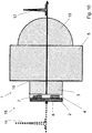
- the lens can form the carrier.
- This embodiment of the antenna 16 is shown in FIG Fig. 9 shown.
- the substrate 3 is therefore attached directly to the lens 14 without the need for an additional carrier will.
- the lens 14 can adjoin the substrate 3 or a fourth adhesion-promoting layer can be arranged between the lens 14 and the substrate 13, which connects the flat side of the lens 14 and the substrate 3 flatly and flush with one another.
- the lens 14 is made of the same material as the substrate 3.
- the photoactive layer 2 and the metal structures 7, 8 of the antenna conductor 6 are constructed in a manner similar to that in the antenna of FIG Fig. 7 .
- the structure of the photoactive layer 2 and the metal structures 7, 8 of the Fig. 6 can be used.
- the antenna 16 shown has a similar structure to the antenna of FIG Fig. 8 and differs only with regard to the arrangement of the metal structures 7, 8 from the antenna of FIG Fig. 8 away.
- the metal structures 7, 8 of the antenna conductor 6 of Fig. 10 are arranged on a side of the photoactive layer 2 facing the substrate 3, while they are in the Fig. 6 are arranged on a side of the photoactive layer facing away from the substrate 3.
- the first adhesion-promoting layer 4 is arranged between the metal structures 7, 8 and the substrate 3 and connects the metal structures 7, 8 with the substrate 3 over a large area.
- the first adhesion-promoting layer 4 thus has a reduced layer thickness in the area of the metal structures 7, 8.
- FIG. 10 An advantage of the in Fig. 10 The arrangement shown is that reflected optical radiation strikes the opaque metal structures 7, 8 and thus does not generate any free charge carriers in the photoactive layer 2. A side of the photoactive layer 2 facing away from the substrate 3 is completely free of coating and is exposed to the ambient air.
- the antennas 16 of the Figures 6-10 are preferred in the terahertz system 20 of FIG Fig. 11 used.
- a method for producing the arrangement 1 or for producing the antenna 16 is described below.
- an auxiliary substrate made of InP is provided. Thereafter the photoactive layer 2 is produced.
- the photoactive layer 2 is produced by epitaxial growth on the InP auxiliary substrate.
- the photoactive layer 2 is usually grown by means of molecular beam epitaxy at a temperature of 200.degree. C. to 450.degree. The temperature is preferably 400 ° C.
- the photoactive layer 2 is preferably doped with a transition metal in a concentration of at least 10 18 cm -3.
- the side of the photoactive layer facing away from the auxiliary substrate can be connected over the entire surface to a silicon wafer with a diameter of at least 2 inches, preferably at least 3 inches and a wafer thickness between 0.2 mm and 1 mm, wherein the first adhesion-promoting layer 4 is used for the connection.
- the silicon wafer and the auxiliary substrate are now located on opposite sides of the photoactive layer 2.
- the auxiliary substrate is then completely removed, preferably by chemical etching. Alternatively, the auxiliary substrate can also be removed mechanically.
- the antenna conductor 6 is contacted with the photoactive layer 2.
- the antenna conductor 6 with the first partial structure 7 and the second partial structure 8 is applied to the photoactive layer 2 in such a way that the two partial structures 7, 8 are spaced from one another and contact the photoactive layer 2.
- the antenna conductor 6 is preferably applied in a so-called lift-off process by means of vapor deposition or sputtering of metal.
- the antenna conductor 6 can be applied immediately before the photoactive layer 2 is connected to the substrate 3 (that is, before the auxiliary substrate is removed) or only after the auxiliary substrate has been removed.
- the photoactive layer 2 can be etched away in areas after the removal of the auxiliary substrate, usually by wet chemical etching processes and dry etching processes.
- the metal structures 7, 8 can then be applied as described above.
- the Mesa structure of the photoactive layer 2 can be produced before connecting the photoactive layer 2 to the silicon wafer.
- the metal structures 7, 8 are then applied to the photoactive layer 2 by vapor deposition or sputtering.
- the first adhesion-promoting layer 4 is then applied to the metal structures 7, 8 and the photoactive layer 2.
- the silicon wafer is connected to the photoactive layer 2 via the layer 4.
- the auxiliary substrate is removed, preferably completely removed.
- a surface passivation for example made of silicon nitride or silicon oxide, can optionally be applied to the photoactive layer 2 and / or the metallic substructures 7, 8.
- the silicon wafer can be cut to size in such a way that a plurality of chips are formed, each having a substrate 3 made of Si, the Adhesion-promoting layer 4, the photoactive layer 2 and the metal structures 7, 8.
- the Si wafer is therefore used for the production of a large number of substrates 3.
- the substrate 3 in the form of a chip at the beginning of the method.
- the substrate 3 is then attached to the carrier 5 or to the lens 14 designed as a carrier. If necessary, the lens 13 is then connected to the carrier 5.
- the method described is particularly suitable for producing the arrangement 1 described above and the antenna 16 described in FIGS. 6-10.
- Features that are only mentioned in relation to the arrangement and the antenna can also be claimed for the method and vice versa.
Landscapes
- Engineering & Computer Science (AREA)
- Microelectronics & Electronic Packaging (AREA)
- Investigating Or Analysing Materials By Optical Means (AREA)
Priority Applications (5)
| Application Number | Priority Date | Filing Date | Title |
|---|---|---|---|
| EP20173549.5A EP3907764A1 (fr) | 2020-05-07 | 2020-05-07 | Agencement pour une antenne permettant de générer ou de recevoir un rayonnement térahertz, antenne, système térahertz ainsi que procédé de fabrication d'un agencement pour une antenne |
| JP2022567210A JP7668819B2 (ja) | 2020-05-07 | 2021-05-05 | テラヘルツ放射を発生または受信するためのアンテナ用のアレンジメント、アンテナ、テラヘルツシステム、及び、アンテナ用のアレンジメントの製造方法 |
| US17/998,096 US12113144B2 (en) | 2020-05-07 | 2021-05-05 | Arrangement for an antenna for generating or receiving terahertz radiation, antenna, terahertz system, and method for producing an arrangement for an antenna |
| EP21723262.8A EP4147278A1 (fr) | 2020-05-07 | 2021-05-05 | Ensemble pour une antenne destinée à générer ou recevoir un rayonnement térahertz, antenne, système térahertz et procédé de fabrication d'un ensemble pour une antenne |
| PCT/EP2021/061881 WO2021224336A1 (fr) | 2020-05-07 | 2021-05-05 | Ensemble pour une antenne destinée à générer ou recevoir un rayonnement térahertz, antenne, système térahertz et procédé de fabrication d'un ensemble pour une antenne |
Applications Claiming Priority (1)
| Application Number | Priority Date | Filing Date | Title |
|---|---|---|---|
| EP20173549.5A EP3907764A1 (fr) | 2020-05-07 | 2020-05-07 | Agencement pour une antenne permettant de générer ou de recevoir un rayonnement térahertz, antenne, système térahertz ainsi que procédé de fabrication d'un agencement pour une antenne |
Publications (1)
| Publication Number | Publication Date |
|---|---|
| EP3907764A1 true EP3907764A1 (fr) | 2021-11-10 |
Family
ID=70617028
Family Applications (2)
| Application Number | Title | Priority Date | Filing Date |
|---|---|---|---|
| EP20173549.5A Withdrawn EP3907764A1 (fr) | 2020-05-07 | 2020-05-07 | Agencement pour une antenne permettant de générer ou de recevoir un rayonnement térahertz, antenne, système térahertz ainsi que procédé de fabrication d'un agencement pour une antenne |
| EP21723262.8A Pending EP4147278A1 (fr) | 2020-05-07 | 2021-05-05 | Ensemble pour une antenne destinée à générer ou recevoir un rayonnement térahertz, antenne, système térahertz et procédé de fabrication d'un ensemble pour une antenne |
Family Applications After (1)
| Application Number | Title | Priority Date | Filing Date |
|---|---|---|---|
| EP21723262.8A Pending EP4147278A1 (fr) | 2020-05-07 | 2021-05-05 | Ensemble pour une antenne destinée à générer ou recevoir un rayonnement térahertz, antenne, système térahertz et procédé de fabrication d'un ensemble pour une antenne |
Country Status (4)
| Country | Link |
|---|---|
| US (1) | US12113144B2 (fr) |
| EP (2) | EP3907764A1 (fr) |
| JP (1) | JP7668819B2 (fr) |
| WO (1) | WO2021224336A1 (fr) |
Families Citing this family (1)
| Publication number | Priority date | Publication date | Assignee | Title |
|---|---|---|---|---|
| CN118487093B (zh) * | 2024-07-15 | 2024-10-29 | 中国科学技术大学 | 一种基于飞秒激光电离各向同性固体介质的光源装置 |
Citations (4)
| Publication number | Priority date | Publication date | Assignee | Title |
|---|---|---|---|---|
| JP2005176156A (ja) * | 2003-12-15 | 2005-06-30 | Nippon Telegr & Teleph Corp <Ntt> | アンテナ集積素子及びその作製方法 |
| US20050215031A1 (en) * | 2004-03-26 | 2005-09-29 | Canon Kabushiki Kaisha | Photo-semiconductor device and method of manufacturing the same |
| DE102007044839A1 (de) | 2007-09-14 | 2009-05-20 | Fraunhofer-Gesellschaft zur Förderung der angewandten Forschung e.V. | Verfahren zum Erzeugen und kohärenten Detektieren von Terahertzstrahlung |
| DE102010049658A1 (de) | 2010-10-25 | 2012-04-26 | Fraunhofer-Gesellschaft zur Förderung der angewandten Forschung e.V. | Effizienz-verbessertes fasergekoppeltes Terahertzsystem |
Family Cites Families (3)
| Publication number | Priority date | Publication date | Assignee | Title |
|---|---|---|---|---|
| JP4476462B2 (ja) * | 2000-03-27 | 2010-06-09 | 株式会社栃木ニコン | 半導体の電気特性評価装置 |
| JP4794878B2 (ja) | 2004-03-26 | 2011-10-19 | キヤノン株式会社 | 光伝導素子 |
| JP6062640B2 (ja) | 2011-03-18 | 2017-01-18 | キヤノン株式会社 | 光伝導素子 |
-
2020
- 2020-05-07 EP EP20173549.5A patent/EP3907764A1/fr not_active Withdrawn
-
2021
- 2021-05-05 JP JP2022567210A patent/JP7668819B2/ja active Active
- 2021-05-05 US US17/998,096 patent/US12113144B2/en active Active
- 2021-05-05 EP EP21723262.8A patent/EP4147278A1/fr active Pending
- 2021-05-05 WO PCT/EP2021/061881 patent/WO2021224336A1/fr not_active Ceased
Patent Citations (4)
| Publication number | Priority date | Publication date | Assignee | Title |
|---|---|---|---|---|
| JP2005176156A (ja) * | 2003-12-15 | 2005-06-30 | Nippon Telegr & Teleph Corp <Ntt> | アンテナ集積素子及びその作製方法 |
| US20050215031A1 (en) * | 2004-03-26 | 2005-09-29 | Canon Kabushiki Kaisha | Photo-semiconductor device and method of manufacturing the same |
| DE102007044839A1 (de) | 2007-09-14 | 2009-05-20 | Fraunhofer-Gesellschaft zur Förderung der angewandten Forschung e.V. | Verfahren zum Erzeugen und kohärenten Detektieren von Terahertzstrahlung |
| DE102010049658A1 (de) | 2010-10-25 | 2012-04-26 | Fraunhofer-Gesellschaft zur Förderung der angewandten Forschung e.V. | Effizienz-verbessertes fasergekoppeltes Terahertzsystem |
Non-Patent Citations (1)
| Title |
|---|
| TAKAHASHI R ET AL: "Ultrafast 1.55-um photoresponses in low-temperature-grown InGaAs/InAlAs quantum wells", APPLIED PHYSICS LETTERS, A I P PUBLISHING LLC, US, vol. 65, no. 14, 3 October 1994 (1994-10-03), pages 1790 - 1792, XP002109073, ISSN: 0003-6951, DOI: 10.1063/1.112870 * |
Also Published As
| Publication number | Publication date |
|---|---|
| EP4147278A1 (fr) | 2023-03-15 |
| WO2021224336A1 (fr) | 2021-11-11 |
| JP7668819B2 (ja) | 2025-04-25 |
| US20240234615A9 (en) | 2024-07-11 |
| JP2023524759A (ja) | 2023-06-13 |
| US12113144B2 (en) | 2024-10-08 |
| US20240136460A1 (en) | 2024-04-25 |
Similar Documents
| Publication | Publication Date | Title |
|---|---|---|
| EP2633286B1 (fr) | Système à térahertz à fibres couplées à efficacité améliorée | |
| EP2185916B1 (fr) | Procédé de génération et de détection cohérente d'un rayonnement térahertz | |
| AT412023B (de) | Verfahren und einrichtung zur elektrooptischen distanzmessung | |
| US10288478B2 (en) | Photoconductive antenna for terahertz waves, method for producing such photoconductive antenna and terahertz time domain spectroscopy system | |
| EP3867974B1 (fr) | Antenne de réception térahertz multicanaux photoconductrice, récepteur, système térahertz et procédé térahertz | |
| EP2901529B1 (fr) | Procédé et dispositif de détermination de la position temporelle relative d'impulsions électromagnétiques | |
| EP3907764A1 (fr) | Agencement pour une antenne permettant de générer ou de recevoir un rayonnement térahertz, antenne, système térahertz ainsi que procédé de fabrication d'un agencement pour une antenne | |
| DE102022133586A1 (de) | Optische messvorrichtung und verfahren | |
| DE102010013751A1 (de) | Vorrichtung zur Laufzeitmessung mit Pulsformung zur Entfernungsbestimmung | |
| DE102011015384B4 (de) | Photoleitendes Antennenarray zum Empfang gepulster Terahertzstrahlung | |
| DE102017213729B4 (de) | Verfahren und Vorrichtung zur Bereitstellung eines Detektionssignals für zu detektierende Objekte | |
| DE102006002732B4 (de) | Photomischdetektor und Verfahren zu dessen Betrieb | |
| WO2023016827A1 (fr) | Procédé et dispositif de mesure lidar à l'aide de sous-impulsions produites par biréfringence dans le résonateur laser | |
| EP2762920A1 (fr) | Procédé de détermination du temps de propagation d'un signal | |
| DE102019100945B4 (de) | Hochfrequenzvorrichtung und zugehöriges Verfahren zum Erzeugen und Erfassen von elektromagnetischer THz-Strahlung | |
| WO2017137589A1 (fr) | Antenne térahertz et procédé pour la fabrication d'une antenne térahertz | |
| EP3417299B1 (fr) | Analyseur de spectre et procédé d'analyse spectrale | |
| DE102008012028A1 (de) | Vorrichtung zur Laser-Doppler-Geschwindigkeitsmessung | |
| DE102013107265B4 (de) | Optoelektronische Hochfrequenzvorrichtung | |
| DE102023120581A1 (de) | Optoelektronischer sensor zum erfassen von objekten in einem überwachungsbereich | |
| WO1993011440A1 (fr) | Procede et dispositif de determination optique de differences de densite d'inversion dans des composants semi-conducteurs | |
| DE102016011383A1 (de) | Photoleitende Antenne zur Erzeugung oder zum Empfang von Terahertz-Strahlung |
Legal Events
| Date | Code | Title | Description |
|---|---|---|---|
| PUAI | Public reference made under article 153(3) epc to a published international application that has entered the european phase |
Free format text: ORIGINAL CODE: 0009012 |
|
| STAA | Information on the status of an ep patent application or granted ep patent |
Free format text: STATUS: THE APPLICATION HAS BEEN PUBLISHED |
|
| AK | Designated contracting states |
Kind code of ref document: A1 Designated state(s): AL AT BE BG CH CY CZ DE DK EE ES FI FR GB GR HR HU IE IS IT LI LT LU LV MC MK MT NL NO PL PT RO RS SE SI SK SM TR |
|
| B565 | Issuance of search results under rule 164(2) epc |
Effective date: 20201023 |
|
| RAP3 | Party data changed (applicant data changed or rights of an application transferred) |
Owner name: FRAUNHOFER-GESELLSCHAFT ZUR FOERDERUNG DER ANGEWANDTEN FORSCHUNG E.V. |
|
| STAA | Information on the status of an ep patent application or granted ep patent |
Free format text: STATUS: THE APPLICATION IS DEEMED TO BE WITHDRAWN |
|
| 18D | Application deemed to be withdrawn |
Effective date: 20220511 |