EP3910285B1 - Scatterometriemessung asymmetrischer strukturen - Google Patents
Scatterometriemessung asymmetrischer strukturen Download PDFInfo
- Publication number
- EP3910285B1 EP3910285B1 EP21175735.6A EP21175735A EP3910285B1 EP 3910285 B1 EP3910285 B1 EP 3910285B1 EP 21175735 A EP21175735 A EP 21175735A EP 3910285 B1 EP3910285 B1 EP 3910285B1
- Authority
- EP
- European Patent Office
- Prior art keywords
- light
- asymmetry
- sample
- mueller matrix
- incident
- Prior art date
- Legal status (The legal status is an assumption and is not a legal conclusion. Google has not performed a legal analysis and makes no representation as to the accuracy of the status listed.)
- Active
Links
Images



Classifications
-
- G—PHYSICS
- G01—MEASURING; TESTING
- G01N—INVESTIGATING OR ANALYSING MATERIALS BY DETERMINING THEIR CHEMICAL OR PHYSICAL PROPERTIES
- G01N21/00—Investigating or analysing materials by the use of optical means, i.e. using sub-millimetre waves, infrared, visible or ultraviolet light
- G01N21/17—Systems in which incident light is modified in accordance with the properties of the material investigated
- G01N21/21—Polarisation-affecting properties
- G01N21/211—Ellipsometry
-
- G—PHYSICS
- G01—MEASURING; TESTING
- G01B—MEASURING LENGTH, THICKNESS OR SIMILAR LINEAR DIMENSIONS; MEASURING ANGLES; MEASURING AREAS; MEASURING IRREGULARITIES OF SURFACES OR CONTOURS
- G01B11/00—Measuring arrangements characterised by the use of optical techniques
- G01B11/02—Measuring arrangements characterised by the use of optical techniques for measuring length, width or thickness
- G01B11/06—Measuring arrangements characterised by the use of optical techniques for measuring length, width or thickness for measuring thickness ; e.g. of sheet material
- G01B11/0616—Measuring arrangements characterised by the use of optical techniques for measuring length, width or thickness for measuring thickness ; e.g. of sheet material of coating
- G01B11/0641—Measuring arrangements characterised by the use of optical techniques for measuring length, width or thickness for measuring thickness ; e.g. of sheet material of coating with measurement of polarization
- G01B11/065—Measuring arrangements characterised by the use of optical techniques for measuring length, width or thickness for measuring thickness ; e.g. of sheet material of coating with measurement of polarization using one or more discrete wavelengths
-
- G—PHYSICS
- G03—PHOTOGRAPHY; CINEMATOGRAPHY; ANALOGOUS TECHNIQUES USING WAVES OTHER THAN OPTICAL WAVES; ELECTROGRAPHY; HOLOGRAPHY
- G03F—PHOTOMECHANICAL PRODUCTION OF TEXTURED OR PATTERNED SURFACES, e.g. FOR PRINTING, FOR PROCESSING OF SEMICONDUCTOR DEVICES; MATERIALS THEREFOR; ORIGINALS THEREFOR; APPARATUS SPECIALLY ADAPTED THEREFOR
- G03F7/00—Photomechanical, e.g. photolithographic, production of textured or patterned surfaces, e.g. printing surfaces; Materials therefor, e.g. comprising photoresists; Apparatus specially adapted therefor
- G03F7/70—Microphotolithographic exposure; Apparatus therefor
- G03F7/70483—Information management; Active and passive control; Testing; Wafer monitoring, e.g. pattern monitoring
- G03F7/70605—Workpiece metrology
- G03F7/70616—Monitoring the printed patterns
- G03F7/70625—Dimensions, e.g. line width, critical dimension [CD], profile, sidewall angle or edge roughness
-
- G—PHYSICS
- G03—PHOTOGRAPHY; CINEMATOGRAPHY; ANALOGOUS TECHNIQUES USING WAVES OTHER THAN OPTICAL WAVES; ELECTROGRAPHY; HOLOGRAPHY
- G03F—PHOTOMECHANICAL PRODUCTION OF TEXTURED OR PATTERNED SURFACES, e.g. FOR PRINTING, FOR PROCESSING OF SEMICONDUCTOR DEVICES; MATERIALS THEREFOR; ORIGINALS THEREFOR; APPARATUS SPECIALLY ADAPTED THEREFOR
- G03F7/00—Photomechanical, e.g. photolithographic, production of textured or patterned surfaces, e.g. printing surfaces; Materials therefor, e.g. comprising photoresists; Apparatus specially adapted therefor
- G03F7/70—Microphotolithographic exposure; Apparatus therefor
- G03F7/70483—Information management; Active and passive control; Testing; Wafer monitoring, e.g. pattern monitoring
- G03F7/70605—Workpiece metrology
- G03F7/70616—Monitoring the printed patterns
- G03F7/70633—Overlay, i.e. relative alignment between patterns printed by separate exposures in different layers, or in the same layer in multiple exposures or stitching
-
- G—PHYSICS
- G01—MEASURING; TESTING
- G01B—MEASURING LENGTH, THICKNESS OR SIMILAR LINEAR DIMENSIONS; MEASURING ANGLES; MEASURING AREAS; MEASURING IRREGULARITIES OF SURFACES OR CONTOURS
- G01B2210/00—Aspects not specifically covered by any group under G01B, e.g. of wheel alignment, caliper-like sensors
- G01B2210/56—Measuring geometric parameters of semiconductor structures, e.g. profile, critical dimensions or trench depth
-
- G—PHYSICS
- G01—MEASURING; TESTING
- G01N—INVESTIGATING OR ANALYSING MATERIALS BY DETERMINING THEIR CHEMICAL OR PHYSICAL PROPERTIES
- G01N21/00—Investigating or analysing materials by the use of optical means, i.e. using sub-millimetre waves, infrared, visible or ultraviolet light
- G01N21/17—Systems in which incident light is modified in accordance with the properties of the material investigated
- G01N21/21—Polarisation-affecting properties
- G01N21/211—Ellipsometry
- G01N2021/213—Spectrometric ellipsometry
-
- G—PHYSICS
- G01—MEASURING; TESTING
- G01N—INVESTIGATING OR ANALYSING MATERIALS BY DETERMINING THEIR CHEMICAL OR PHYSICAL PROPERTIES
- G01N21/00—Investigating or analysing materials by the use of optical means, i.e. using sub-millimetre waves, infrared, visible or ultraviolet light
- G01N21/17—Systems in which incident light is modified in accordance with the properties of the material investigated
- G01N21/21—Polarisation-affecting properties
- G01N21/211—Ellipsometry
- G01N2021/214—Variangle incidence arrangement
Definitions
- Scatterometry has been used extensively for the characterization of critical dimensions (CD) and detailed side-wall profiles of periodic structures in microelectronics fabrication processes. Scatterometry can provide accurate and high-precision measurement for 2D and 3D structures used in integrated circuits.
- Various experimental configurations e.g., normal incident broadband reflectance spectroscopy, spectroscopic ellipsometry, and angular scatterometry measurement, have been developed to collect light signals diffracted from periodic structures. So far the majority of measurements were applied for symmetric gratings. In most cases devices are designed to be symmetric although errors could occur during fabrication processing and result in undesired asymmetry.
- asymmetry is alignment or overlay error.
- overlay targets are used to determine if the pattern produced in one layer is adequately aligned with the pattern in an underlying or previously patterned layer.
- This overlay metrology problem becomes particularly difficult at submicrometer feature sizes where overlay tolerances are reduced to provide reliable semiconductor devices.
- Fig. 1 illustrates a conventional box-in-box overlay target 2 used with conventional image based overlay metrology methods.
- Target 2 is formed by producing an etched box 4 in first material layer on a substrate and another box 8 in a second material layer, or on the same layer.
- the target 2 is produced on the wafer off the chips, e.g., in the scribe lines between chips.
- the overlay target 2 is imaged to determine whether the second layer is properly aligned with the first layer.
- Other image based overlay targets such as a bar-in-bar target, are produced and imaged in a similar fashion.
- high magnification imaging is used to measure image based overlay targets, such as target 2.
- Conventional imaging devices unfortunately, suffer from disadvantages such as lack of sensitivity to vibration and cost.
- image based overlay targets are outside the chip, e.g., in a scribe line and are larger scale than most current and future devices. Consequently, the overlay errors measured by image based overlay targets are not suitable to represent the true overlay error in the actual device area.
- diffraction based overlay measurements are performed using scatterometry, which relies on diffracting targets, such as diffraction gratings. Similar to image based overlay measurements, diffraction based overlay measurements require specialized off-chip targets. Diffraction based overlay measurements utilize the diffraction pattern produced by the target to determine overlay. The off-chip overlay targets use multiple overlying structures with different designed in offsets are used to determine the overlay error differentially, which requires a large amount of real estate on the wafer. Moreover, the off-chip location of the targets again may not accurately represent the overlay error in the actual device area.
- Nano-imprint lithography for patterned media.
- Patterned media has been proposed to extend the hard disk drive magnetic recording density beyond 1 Tbit/inch 2 during the last couple of years.
- the implementation of patterned media requires the nano-imprint lithography (NIL, either thermal- or UV-NIL) to pattern the surface of the media.
- NIL nano-imprint lithography
- the template is lowered and made contact with the pre-deposited disk substrate, and the region between the substrate and the topography of the imprint template is completely filled with imprint resist by the capillary action.
- the mirror image is replicated on the disk.
- tilted resist gratings are frequently seen on the disk after imprint.
- the non-expected tilting resist profile causes difficulties to the downstream processes or even makes them fail. Detect the tilting orientation and amount is becoming critical to improve the imprint process and ensure the success for patterned media.
- Metrology techniques used to conventionally measure an asymmetry such as tilt include cross-sectional scanning electron microscopy (SEM) imaging, but this method is destructive and the sample is destroyed after inspection.
- Atomic force microscopy (AFM) scans can provide partial information of grating profile as long as the AFM tip is able to reach the trench bottom.
- AFM Atomic force microscopy
- Another downside factor of cross-sectional SEM and AFM is the slow throughput. Both methods are time consuming and hard to inspect the whole surface of the sample.
- TATIANA NOVIKOVA ET AL "Application of Mueller polarimetry in conical diffraction for critical dimension measurements in microelectronics", APPLIED OP, OPTICAL SOCIETY OF AMERICA, WASHINGTON, DC; US, (20060601), vol. 45, no. 16, pages 3688 - 3697 describes the potential of spectral Mueller polarimetry in conical diffraction for the characterization of 1D gratings, with particular emphasis on small critical dimensions (CDs).
- Mueller matrix spectra were taken in the visible(450-700 nm) wavelength range on a photoresist grating on a Si substrate with70/240 nm CD/period nominal values, set at nine different azimuthal angles.
- US2006/274310 describes a system using ellipsometer configurations to measure the partial Mueller matrix and the complete Jones matrix of a system that may be isotropic or anisotropic.
- Two or more signals which do not necessarily satisfy any symmetry assumptions individually, are combined into a composite signal which satisfies a symmetry assumption.
- the individual signals are collected at two or more analyzer angles.
- Symmetry properties of the composite signals allow easy extraction of overlay information for any relative orientation of the incident light beam with respect to a ID grating target, as well as for targets comprising general 2D gratings.
- Signals of a certain symmetry property also allow measurement of profile asymmetry.
- only signals which satisfy a symmetry assumption are measured.
- a single polarization element serves as polarizer and analyzer or an analyzing prism simultaneously collects two polarization components of reflected light.
- US2007/263219 descibes a polarimetric measurement device of a planar object carrying patterns repeated regularly and forming the lines of a grid.
- a first measurement is carried out at zero order, under an angle of incidence theta1 and for a first azimuthal angle phi1
- a second measurement at least is carried out at zero order, under an angle of incidence theta2 and for a second azimuthal angle phi2
- the polarization of the incident beam is modulated and the polarization of the reflected beam is analyzed for each measurement
- theoretical polarimetric data is calculated for a model object of the real object, the model object including parameters adjustable using a formalism of electromagnetism.
- An iterative comparison of the measurements is conducted with the theoretical polarimetric data for different values of the adjustable parameters.
- JIE LI ET AL "Scatterometry Measurement of Asymmetric Gratings" describes that a problem with conventional optical scatterometry techniques lies in the lack of capability to distinguish between left and right asymmetries.
- the authors investigate the possibility of measuring grating asymmetry using Mueller matrix spectroscopic ellipsometry (MM-SE).
- MM-SE Mueller matrix spectroscopic ellipsometry
- a patterned hard disk prepared by nano-imprint technique is used for the study.
- the relief image on the disk sometimes has asymmetrical sidewall profile, presumably due to the uneven separation of the template from the disk.
- the undesired tilting resist profile causes difficulties to the downstream processes or even makes them fail.
- Cross-section SEM reveals that the asymmetrical resist lines are typically tilted towards the outer diameter direction.
- the simulation and experimental data show that certain Mueller matrix elements are proportional to the direction and amplitude of profile asymmetry, providing a direct indication to the sidewall tilting.
- the tilting parameter can be extracted using rigorous optical critical dimension (OCD) modeling or calibration method.
- OCD optical critical dimension
- the authors demonstrate that this technique has good sensitivity for measuring and distinguishing left and right asymmetry caused by sidewall tilting, and can therefore be used for monitoring processes, such as lithography and etch processing, for which symmetric structures are desired.
- Optical techniques can be used to detect and quantify the asymmetric grating profile.
- Conventional optical scatterometry techniques have the problem with asymmetric lines due to the lack of capability of distinguishing between left and right asymmetries.
- Asymmetry metrology is performed by generating at least a portion of a Mueller matrix and analyzing the Mueller matrix, e.g., at least the off-diagonal elements of the Mueller matrix, to determine the value of the asymmetry, such as the offset between two overlying structures or the tilt of a diffraction grating or isolated structure.
- the Mueller matrix may be generated using, e.g., a spectroscopic or angle resolved ellipsometer that may include a rotating compensator.
- the Mueller matrix may be analyzed by fitting at least a portion of the elements to the Mueller matrix elements or by fitting the combined anti-symmetric off-diagonal elements to a calibrated linear response.
- Using the Mueller matrix in asymmetry metrology advantageously permits the use of in-chip structures as the asymmetry target, thereby avoiding the need for special off-chip targets.
- Fig. 2 illustrates an ellipsometer 100 that may be used to perform an asymmetry measurement of a structure on a sample based on at least a portion of the Mueller matrix.
- the sample 101 illustrated in Fig. 2 includes two overlaying diffraction patterns 101top and 101bottom, where the asymmetry measurement may be a measurement of the overlay error in the overlaying diffraction patterns 101top and 101bottom.
- Ellipsometer 100 may be used with different samples, and may make different asymmetry measurements.
- Ellipsometer 100 is a rotating compensator ellipsometer 100 that performs a diffraction based measurement on the sample 101.
- the ellipsometer 100 includes a polarization state generator (PSG) 102 and a polarization state detector (PSD) 112.
- the PSG 102 produces light having a known polarization state and is illustrated as including two broadband light sources 104 and 106, e.g., a Xenon Arc lamp and a Deuterium lamp, respectively, to produce light with a range of 200-100nm.
- a beam splitter 108 combine the light from the light sources 104, 106 and a polarizer 110 produces the known polarization state. It should be understood that additional, different, or fewer light sources may be used if desired.
- ellipsometer 100 may be monochromatic, with a variable angle of incidence to provide angle resolved measurements.
- the PSD 112 includes a polarizing element, referred to as an analyzer 114, a spectrometer 116 and a detector 118, which may be, e.g., a cooled CCD array.
- the analyzer 114 is illustrated as being coupled to the spectrometer 116 and detector 118 via a fiber optic cable 120. It should be understood that other arrangements are possible, such as directly illuminating the spectrometer 116 from the analyzer 114 without the fiber optic cable 120.
- the ellipsometer 100 is illustrated with two rotating compensators 122 and 124 between the PSG 102 and PSD 112. If desired, the ellipsometer 100 may use a single rotating compensator 122 or 124, e.g., between the PSG 102 and the sample 101 or between the sample 101 and the PSD 112, respectively.
- the ellipsometer 100 may further include focusing elements 126 and 128 before and after the sample 101, as illustrated in Fig. 2 .
- the focusing elements may be, e.g., refractive or reflective lenses.
- the ellipsometer 100 obliquely illuminates the sample 101, e.g., at a non-zero value of ⁇ with respect to surface normal 126.
- the ellipsometer 100 may illuminate the sample 101 at an angle between 50° to 85°, for example at 65°, but other angles may be used if desired.
- the angle of incidence may be varied to derive an angle resolved measurement.
- the plane of incidence 113 is at an angle ⁇ with respect to the direction of periodicity of the diffraction pattern on the sample 101, identified in Fig. 2 as along axis X.
- the angle ⁇ may be 0°, 90°, or anywhere in between, e.g., 45°.
- the ellipsometer may be a M2000 ellipsometer produced by JA Woollam Co., Inc.
- the detector 118 is coupled to a computer 130, which includes a processor 132 with memory 134, as well as a user interface including e.g., a display 138 and input devices 140.
- a computer-usable medium 142 having computer-readable program code embodied may be used by the computer 130 for causing the processor to control the device 100 and to perform the functions including the analysis described herein.
- the data structures and software code for automatically implementing one or more acts described in this detailed description can be implemented by one of ordinary skill in the art in light of the present disclosure and stored, e.g., on a computer readable storage medium 142, which may be any device or medium that can store code and/or data for use by a computer system such as processor 132.
- the computer-usable medium 142 may be, but is not limited to, magnetic and optical storage devices such as disk drives, magnetic tape, compact discs, and DVDs (digital versatile discs or digital video discs).
- a communication port 144 may also be used to receive instructions that are used to program the computer 130 to perform any one or more of the functions described herein and may represent any type of communication connection, such as to the internet or any other computer network.
- the functions described herein may be embodied in whole or in part within the circuitry of an application specific integrated circuit (ASIC) or a programmable logic device (PLD), and the functions may be embodied in a computer understandable descriptor language which may be used to create an ASIC or PLD that operates as herein described.
- ASIC application specific integrated circuit
- PLD programmable logic device
- Ellipsometry typically examines the changes in the p- and s- components of light caused by reflection or transmission from a sample. For example, light having a known polarization state from the PSG 102 is produced and incident on the sample and the resulting change in the polarization state is measured by the PSD 112.
- E p and E s are the electrical vectors for the respective parallel and perpendicular components of the elliptically polarized incident light and E' p and E' s are the parallel and perpendicular components, respectively, of the elliptically polarized reflected light, and R p and R s are the reflection coefficients of the sample for the parallel and perpendicular components of light.
- a diffraction based measurement of a sample is based on the spectral response of the scattered light to the structure of the sample.
- the response is typically measured ellipsometrically by monitoring the change in ⁇ (the ratio of R p /R s ) and ⁇ (phase difference between R p and R s ).
- ⁇ the ratio of R p /R s
- ⁇ phase difference between R p and R s
- one or more layers may be between the overlying diffraction patterns 101top and 101bottom or alternatively, the patterns may be on the same level, as illustrated in Figs. 3F and 3G where the bottom layer 101bottom is the first layer deposited and the top layer 101top is the subsequent deposited layer, which is deposited on the same level as bottom layer 101bottom.
- Fig. 3F illustrates a perspective view of a structure in which the first deposited layer 101bottom is e.g., etched into silicon with surrounding space filled with silicon dioxide, then in a second etch step another structure is etched in the bottom layer 101bottom and material deposited to form top layer 101top, where an overlay error exists between the first and second layers 101bottom and 101top.
- Fig. 3F illustrates a perspective view of a structure in which the first deposited layer 101bottom is e.g., etched into silicon with surrounding space filled with silicon dioxide, then in a second etch step another structure is etched in the bottom layer 101bottom and material deposited to form top layer 101top, where an
- 3G illustrates a double patterned sample 101 where the grating has lines 101bottom and 101top on the same level, where an overlay error e is evident.
- a diffraction based overlay target such as sample 101 illustrated in Figs. 3A , 3F, and 3G
- a model of the overlying diffraction patterns 101top and 101bottom are produced with an overlay error, along with other parameters, such as height, CD, and sidewall angle.
- the measured ellipsometric data is compared to the calculated ellipsometric data to determine if there is a good fit. If the measured and calculated ellipsometric data have a good fit, then the model of the sample 101 is considered to be an accurate representation of the sample including the overlay error.
- a different model of the sample 101 e.g., with a different overlay error and/or other parameters, along with corresponding calculated ellipsometric data is obtained, e.g., either from a library or in a real-time calculation, and compared with the measured ellipsometric data. This process is repeated until a good fit is achieved.
- Another diffraction based overlay metrology method uses a plurality of targets, each with a slightly different designed in offset. A differential analysis can then be performed using the measured results from the plurality of targets, thereby avoiding the need to model the target and fit the measurement.
- both conventional techniques for diffraction based overlay metrology requires a specially designed target, which must be located outside of the die area, e.g., in a scribe line.
- the target designs typically are two-orders of magnitude larger in line and space dimensions than the in-die devices. Consequently, the measured overlay from the specially designed remote targets may not accurately represent the overlay error within the die.
- Figs. 3B and 3C illustrate a one-dimensional grating structure 101 grating , which may be found in an microelectronic device or in a hard disk patterned media, e.g., in the form of patterned tracks.
- the structure shown in Figs. 3B and 3C is typical for an imprint hard disk at the litho patterning step, e.g., for a 350k TPI disk, which may have a pitch of 73nm, a critical dimension (CD) of 48nm and a height of 60nm.
- CD critical dimension
- gratings In normal processing, symmetric gratings are desired as shown in Fig. 3B .
- the gratings may be tilted, as illustrated in Fig. 3B.
- the grating 100 grating may tilt to the left as well.
- the grating structure may tilt to left at some locations on the disk and tilt to the right at other locations.
- FIG. 3D illustrates an asymmetrical isolated structure 101 isolated , e.g., with a left tilt, which ellipsometer 100 may be used to measure the asymmetry.
- asymmetry of the structure may be detected in more than one direction, e.g., measurable asymmetry may exist in both the x and y directions, or non-orthogonal directions.
- Fig. 3E illustrates a side view of structure 101 grating where the front side wall angle SWA F and back side wall angle SWA B may be measured along with the right and left side wall angles.
- structure 101 grating in Fig. 3E may be in a bit pattern media, where the measurable asymmetry of islands may be present to the inside or outside of the disk while another measureable asymmetry may be present at the leading or trailing edge of the island.
- the asymmetry of a structure including overlay error or tilt
- the use of the Mueller matrix allows measurement of asymmetry without using dedicated targets. Accordingly, overlay error, for example, may be measured using in die structures without using dedicated overlay targets.
- overlay error for example, may be measured using in die structures without using dedicated overlay targets.
- in die devices to measure asymmetry such as overlay error, a significant savings in real estate on the sample is possible because no special targets are needed, e.g., in the scribe line. Consequently, other types of targets may be placed in the scribe line or more dies may be produced on a wafer. Much more sophisticated sampling scheme is also possible, including direct in-die measurement, whereas metrology on the scribe lines is limited to a per die sampling rate.
- the Jones matrix depends on the angle of incidence, azimuth, wavelength as well as structural details of the sample.
- the diagonal elements describe the complex reflectance (amplitude & phase) for polarization orthogonal (r ss ) and parallel (r pp ) to the plane incidence defined by the illumination and collection arms.
- the off-diagonal terms r sp and r pp are related to polarization conversion between s and p polarization states in the presence of sample anisotropy.
- the Jones matrix J elements are not easily obtained experimentally.
- the elements of the 4x4 Mueller matrix M can be derived experimentally.
- the Mueller matrix is measured by the ellipsometer 100, and the Jones matrix is calculated from first principles for a given sample. So to compare the theoretical calculation to the experimental data one needs to convert the Jones matrix to Mueller matrix.
- the first three rows of the Mueller matrix M can be obtained, which can be used to determine an asymmetry.
- an ellipsometer with a rotating polarizer 110 and analyzer 114 and no rotating compensators can be used to experimentally determine the nine elements in the first three rows and first three columns of the Mueller matrix M , which may be used to adequately determine an asymmetry.
- the obtained signal at the detector is a time dependent intensity.
- the Mueller matrix elements are sensitive to the profile details of the structures as well as any asymmetries present, e.g. any misalignment between objects at different levels in the structure or tilting of the structure.
- the Mueller matrix can be used for the detection of asymmetries due to the fact that the Jones cross-reflection coefficients, i.e., r ps and r sp in equation 5 are anti-symmetric for symmetric structures.
- these off-diagonal elements are sensitive to the sign of the tilt parameter ⁇ SWA as well as the amplitude of the tiling and can therefore be used to not only distinguish between left-tilting and right-tilting, but provide a measurement of the amount of tilting.
- Overlaying structures 254 illustrated as a top structure (solid line) and a bottom structure (dotted line), are located within a die. Each die 252 or a plurality of dies 252 may be measured. Moreover, a plurality of locations within the die 252 may be measured.
- Fig. 5B illustrates an imprint hard disk 260 that includes a plurality of grating lines 262, all within the active area of the disk 260.
- the phase of the light may be variably altered using one or both of the rotating compensators 122 and 124 (204), which is useful for determining the first three rows or all four rows of the Mueller matrix. A sufficient number of elements of the Mueller matrix may be determined without the use of rotating compensators, and thus, step 204 may be skipped if desired.
- the light is analyzed using analyzer 114 to polarize the light with a known polarization state (206).
- the analyzed light is detected, e.g., by spectrometer 116 and detector 118 (208). Using the detected light, at least a partial Mueller matrix is generated (210).
- At least the off-diagonal coefficients of the Mueller matrix are analyzed to evaluate the asymmetry of the structure (212), such as alignment, overlay error, or tilting, and the result is stored or displayed (214).
- the off-diagonal coefficients of the Muller matrix may be analyzed by fitting the measured off-diagonal coefficients of the Muller matrix to modeled off-diagonal coefficients of the Muller matrix. If desired, all of the Mueller matrix coefficients, i.e., not only the off-diagonal coefficients may be analyzed. A real-time analysis may be used in which the model parameters are adjusted through non-linear regression or, alternatively, a library may be used.
- the off-diagonal coefficients of the Muller matrix may be analyzed using a calibrated linear response of measured or modeled off-diagonal coefficients of the Muller matrix.
- FIG. 6 illustrates a top plan view of a portion of an in-chip structure 300 that can be measured for overlay error.
- the structure 300 is a portion of a DRAM device and includes overlying structures including a shallow trench isolation (STI) array of islands 302 at a bottom layer and photo-resist lines 304 at the top layer, with several thin film layers in between.
- STI shallow trench isolation
- the silicon islands 302 are arranged in a non-orthogonal lattice and are rotated with respect to the horizontal axis.
- the space surrounding the silicon islands 302 is filled with silicon dioxide.
- the structure 300 may include materials between the islands 302 and the resist lines 304, such as a silicon oxi-nitride layer and anti-reflective coating layer.
- the resist lines 304 are formed over the top of the STI structure.
- the on-chip device structure 300 may be used as an overlay target by exploiting the breaking of symmetry using the Mueller matrix metrology. It should be understood that the Muller matrix metrology may be used with other on-chip devices besides the particular DRAM structure illustrated, including flash memory and logic structures, as well as off-chip diffraction based overlay targets, such as that illustrated in Fig. 3A .
- Fig. 7 illustrates the spectral response for combination of two off-diagonal, cross-reflection Mueller matrix elements (M 13 +M 31 ) to different overlay shifts between top and bottom layers, ranging from +15nm to -15nm, in structures similar to structure 300 shown in Fig. 6 .
- the Muller matrix is adimensional and is bound to the [-1,1] interval.
- the structures used to produces the experimental response were produced using varying intentional overlay displacements for the structure across the diameter of a 300mm silicon wafer.
- Each curve in Fig. 7 corresponds to a different overlay shift in the ⁇ 15nm range. From equation 11, the amplitude of M 13 +M 31 directly corresponds to the asymmetry induced by the overlay error in the structures.
- Fig. 8 illustrates the spectral response averaged over the 245-265nm wavelength range for the overlay shift. As can be seen, the mean response is nearly linear within the ⁇ 15nm range of overlay error.
- Fig. 9 illustrates a set of measured and fit spectra for 11 Mueller matrix elements, i.e., the first three rows, measured by a spectroscopic ellipsometer 100 using a single rotating compensator 122 for a structure similar to structure 300 shown in Fig. 6 .
- the spectra illustrated in Fig. 9 are wavelength resolved as a spectroscopic ellipsometer is used. If desired, an angle resolved measurement may alternatively be used.
- the Mueller matrix element M 11 is defined as 1 and is therefore not shown.
- the spectra for Mueller matrix elements M 13 and M 31 are nearly anti-symmetric, as are the spectra for Mueller matrix elements M 23 and M 32 .
- the change induced by the overlay shift in the sample structure is relatively small compared to the amplitude in the spectra for the cross reflection coefficients of the Muller matrix, e.g., M 13 , M 31 and M 23 , M 32 .
- Figs. 3B , 3C, and 3D Another form of asymmetry that may be measured is the tilting of a structure, as illustrated in Figs. 3B , 3C, and 3D , which may be found, e.g., on an imprint hard disk, such as disk 260 shown in Fig. 5B .
- an angle of incidence of 65° from normal may be used with the plane of incidence at an azimuth angle of 90°, also referred as conical mount because all diffracted orders of reflected beams are on the surface of a cone about the direction of the grating lines.
- Fig. 10 illustrates the Mueller matrix elements for simulations performed using NanoDiffractTM software with an RCWA algorithm. The structure is similar to that shown in Fig.
- the remaining Mueller matrix off-diagonal elements, M 13 , M 14 , M 23 , M 24 , M 31 , and M 32 are not only sensitive to the sign of tilt ⁇ SWA , and thus can distinguish left-tilting from right-tilting, but is also sensitive to the amplitude of the tilt.
- the direction (negative or positive) of the deviation indicates the direction of the tilting (left or right).
- the amplitude of the spectral deviation from zero is proportional to the amplitude of the tilting. Accordingly, this method enables detection of grating asymmetry without the need of structural and optical details and modeling procedure involved in typical OCD metrology.
- the off-diagonal coefficients of the Muller matrix may be analyzed (212 in Fig. 4 ) by fitting the measured off-diagonal coefficients of the Muller matrix to modeled off-diagonal coefficients of the Muller matrix or by fitting the measured off-diagonal coefficients of the Muller matrix to a calibrated linear response of measured or modeled off-diagonal coefficients of the Muller matrix.
- Fig. 12 illustrates analyzing the off-diagonal coefficients of the Muller matrix using a modeling technique.
- a model of the sample is produced (402), e.g., using NanoDiffract TM from Nanometrics Incorporated.
- the model for a structure with an asymmetry such as overlay error may include includes floating parameters that include the overlay error, CD, height and sidewall angle of the bottom and top grating elements, e.g., islands 302 and lines 304, as well as the thickness of any intervening layers.
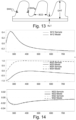
- a model for a structure with an asymmetry such as tilt, such as that illustrated in Fig. 13 may include floating parameters including left and right sidewall angle (SWA L , SWA R ), grating height (GHT), grating bottom critical dimension (BCD), and remaining layer thickness (RLT).
- At least a partial Mueller matrix is calculated for the modeled sample, including the off-diagonal coefficients, such as M 13 , M 31 and M 23 , M 32 (404).
- the Muller matrix may be calculated using a rigorous electromagnetic model, such as Rigorous Couple Wave Analysis (RCWA), which may be performed by NanoDiffract TM from Nanometrics Incorporated.
- Elements in the calculated Mueller matrix, including at least the off-diagonal coefficients are compared to the corresponding elements in the measured Mueller matrix, e.g., that was generated in step 210 in Fig. 4 (406). If desired, all of the elements or a partial set of the elements in the Mueller matrix that have been measured and calculated may be fitted.
- the mean square error between the calculated and the measured Mueller matrix elements may be calculated, e.g., the sum of all the errors squared, and compared to a threshold value or is minimized.
- the goodness of fit is then determined (408), where an acceptable fit indicates that the modeled sample, including the modeled asymmetry as well as the other floating parameters, accurately describes the actual measured sample and the results are then stored or displayed (412). If the fit is not acceptable, the measured Mueller matrix is compared to a calculated Mueller matrix for a different model of the sample, e.g., in which one of the floating parameters has been changed (410). This process is repeated until an acceptable fit is achieved.
- Fig. 9 illustrates is an example of a set of measured and fit spectra for 11 Mueller matrix elements for an asymmetry measurement in the form of overlay error. As can be seen in Fig. 9 , a good agreement for the experimental spectra and the theoretical spectra can be achieved and, thus, the overlay error can be determined.
- Fig. 14 illustrates a set of measured and fit spectra for 5 Mueller matrix elements, specifically M 12 , M 33 , M 34 , M 23 , and M 32 for an asymmetry measurement in the form of tilt.
- the measured data was obtained with a spectroscopic ellipsometer 100 and the fit spectra was generating using a model, such as that illustrated in Fig. 13 , built to describe the grating structure using NanoDiffract software.
- a good agreement for the experimental spectra and the theoretical spectra can be achieved.
- the individual sidewall angles SWA L and SWA R can be determined, from which the tilt ⁇ SWA can be calculated as the difference between the sidewall angles SWA L and SWA R .
- Fig. 15 illustrates analyzing the off-diagonal coefficients of the Muller matrix using a calibrated linear response.
- at least partial Mueller matrices are determined for a plurality of samples with varying values of the asymmetry, e.g., overlay error or tilt (452).
- the overlay offsets for the samples may incrementally vary over ⁇ 15nm range from the nominal offset. The range and incremental variation in the overlay offsets is dependent on the sample, including the CD, as well as the expected variation in overlay during production.
- the sidewall angles or tilt ⁇ SWA of the sample may incrementally vary over a ⁇ 22° range from the symmetrical value of ⁇ SWA 0°, as illustrated in Figs. 10 and 11 .
- the Mueller matrices may be generated mathematically, e.g., through modeling and calculating the Mueller matrices, or empirically, e.g., by producing a number of samples with varying values of asymmetry with a known magnitude and measuring the Mueller matrices.
- non-offset parameters such as CD, height and sidewall angle
- linear combinations e.g., M 13 +M 31 are second order effects and can be neglected for small variations.
- a calibrated linear response for the cross-reflection coefficients is generated based on the determined Mueller matrices (454).
- the calibrated linear response may be formed by generating a linear fit for the average spectral response to the asymmetry within the most sensitive portion of the spectrum or the entire spectrum.
- the linear response may be formed by the individual Mueller matrix coefficients, as illustrated in Fig. 11 or by combining the anti-symmetric cross-reflection coefficients (e.g., M 13 +M 31 and/or M 23 +M 32 ), as illustrated in Fig. 8 . If desired, combination of the cross-reflection coefficients other than the sum may be used to form the linear response.
- the off-diagonal coefficients from the measured Mueller matrix are then compared to the calibrated linear response to determine the value of the asymmetry for the measured sample (456) and the result is stored or displayed (458).
- the spectral response for the same individual or combination of off-diagonal coefficients is produced for the measured Mueller matrix elements.
- the overlay shift would be approximately 8.9nm.
- the alignment or overlay of two layers can be accurately measured.
- the alignment or overlay can be determined using periodic structures of devices on the chip as the measurement target, as opposed to using special off-chip targets.
- a single off-chip periodic target may be used to determine overlay, thereby reducing space requirements compared to conventional systems that use multiple periodic targets with variations in a designed in offset.
Landscapes
- Physics & Mathematics (AREA)
- General Physics & Mathematics (AREA)
- Health & Medical Sciences (AREA)
- Life Sciences & Earth Sciences (AREA)
- Chemical & Material Sciences (AREA)
- Analytical Chemistry (AREA)
- Biochemistry (AREA)
- General Health & Medical Sciences (AREA)
- Immunology (AREA)
- Pathology (AREA)
- Investigating Or Analysing Materials By Optical Means (AREA)
Claims (12)
- Verfahren zum Bestimmen einer Asymmetrie in einer Struktur (212) auf einer Probe (101), das Verfahren umfassend:Erzeugen polarisierten Lichts (202), das auf die Struktur auf der Probe auftrifft;Analysieren des Lichts (206), nachdem das Licht auf die Struktur auf der Probe aufgetroffen ist;Erfassen des Lichts (208) nach dem Analysieren des Lichts;Generieren mit einem Prozessor (132) mindestens einer partiellen Müller-Matrix (210) unter Verwendung des erfassten Lichts;Analysieren mit dem Prozessor der mindestens der partiellen Mueller-Matrix (212), um die Asymmetrie in der Struktur zu bestimmen, wobei das Analysieren mit dem Prozessor der mindestens der partiellen Mueller-Matrix, um die Asymmetrie der Struktur zu bestimmen, ein Verwenden der antisymmetrischen Eigenschaften mindestens eines Satzes antisymmetrischer nichtdiagonaler Elemente der Mueller-Matrix für mehrere Strukturen, die bekannte Asymmetrien aufweisen, und der mindestens der partiellen Mueller-Matrix, um die Asymmetrie der Struktur zu bestimmen, umfasst; wobei der mindestens eine Satz antisymmetrischer nichtdiagonaler Elemente Kreuzpolarisationsremissionskoeffizienten sind.
- Verfahren nach Anspruch 1, ferner umfassend ein Durchgehenlassen des Lichts durch einen rotierenden Kompensator, bevor das Licht auf die Probe auftrifft oder nachdem das Licht auf die Probe aufgetroffen ist.
- Verfahren nach Anspruch 2, wobei das Licht durch einen rotierenden Kompensator durchgelassen wird, bevor das Licht auf die Probe auftrifft, das Verfahren ferner umfassend das Durchgehenlassen des Lichts, nachdem das Licht auf die Probe aufgetroffen ist, durch einen zweiten rotierenden Kompensator und das Generieren einer vollständigen Müller-Matrix unter Verwendung des erfassten Lichts.
- Verfahren nach Anspruch 1, wobei die Probe ein Halbleiterwafer (250) ist und die Struktur eine In-Chip-Struktur ist.
- Verfahren nach Anspruch 1, wobei die Probe mindestens eines von einem Festplatten(260)-gemusterten Medium ist und die Struktur mindestens eine von gemusterten Spuren und gemusterten Inseln und einer mikroelektronisches Vorrichtung umfasst.
- Verfahren nach Anspruch 1, wobei die Struktur ein erstes periodisches Muster (101top), das ein zweites periodisches Muster (101bottom) überlagert, einschließt, und die bestimmte Asymmetrie in der Struktur einen Überlagerungsfehler umfasst.
- Verfahren nach Anspruch 1, wobei die Struktur ein erstes Muster (101top) und ein zweites Muster (101bottom) auf derselben Ebene einschließt und die bestimmte Asymmetrie in der Struktur die Asymmetrie zwischen dem ersten Muster und dem zweiten Muster umfasst.
- Verfahren nach Anspruch 1, wobei die Struktur mindestens eines von einem periodischen Muster (101grating) und einer isolierten Struktur (101 isolated) einschließt.
- Verfahren nach Anspruch 1, wobei das polarisierte Licht mindestens eines von mehreren Wellenlängen und mehreren Autreffwinkeln umfasst.
- Verfahren nach Anspruch 1, wobei die bestimmte Asymmetrie in der Struktur mindestens eines von asymmetrischen Seitenwandwinkeln und Neigung der Struktur umfasst.
- Verfahren nach Anspruch 1, wobei die bestimmte Asymmetrie in zwei Richtungen besteht.
- Einrichtung zum Messen der Asymmetrie einer Struktur (212) auf einer Probe (101), die Einrichtung umfassend:einen Polarisationszustandsgenerator (110) zum Erzeugen polarisierten Lichts, das auf die Struktur auftreffen soll;einen Polarisationszustandsdetektor (114, 118) zum Analysieren und Erfassen des Lichts, nachdem das Licht auf die Struktur aufgetroffen ist, und zum Generieren von Signalen als Reaktion auf das erfasste Licht;einen Prozessor (132), der gekoppelt ist, um die Signale von dem Polarisationszustandsdetektor zu empfangen, wobei der Prozessor konfiguriert ist, um unter Verwendung der Signale von dem Polarisationszustandsdetektor mindestens eine partielle Mueller-Matrix (210) zu generieren und zum Analysieren der mindestens der partiellen Mueller-Matrix konfiguriert ist, um die Asymmetrie der Struktur durch Verwenden der antisymmetrischen Eigenschaften mindestens eines Satzes antisymmetrischer nichtdiagonaler Elemente der Mueller-Matrix für mehrere Strukturen, die bekannte Asymmetrien aufweisen, und der mindestens der partiellen Mueller-Matrix, um die Asymmetrie der Struktur zu bestimmen; wobei der mindestens eine Satz antisymmetrischer nichtdiagonaler Elemente Kreuzpolarisationsremissionskoeffizienten sind.
Priority Applications (1)
| Application Number | Priority Date | Filing Date | Title |
|---|---|---|---|
| EP25177712.4A EP4650733A3 (de) | 2009-10-07 | 2010-09-22 | Messung asymmetrischer strukturen mittels scatterometrie |
Applications Claiming Priority (5)
| Application Number | Priority Date | Filing Date | Title |
|---|---|---|---|
| US24943909P | 2009-10-07 | 2009-10-07 | |
| US26031409P | 2009-11-11 | 2009-11-11 | |
| US12/696,974 US8525993B2 (en) | 2009-10-07 | 2010-01-29 | Scatterometry measurement of asymmetric structures |
| PCT/US2010/049878 WO2011043930A1 (en) | 2009-10-07 | 2010-09-22 | Scatterometry measurement of asymmetric structures |
| EP10822422.1A EP2486378B1 (de) | 2009-10-07 | 2010-09-22 | Scatterometriemessung asymmetrischer strukturen |
Related Parent Applications (1)
| Application Number | Title | Priority Date | Filing Date |
|---|---|---|---|
| EP10822422.1A Division EP2486378B1 (de) | 2009-10-07 | 2010-09-22 | Scatterometriemessung asymmetrischer strukturen |
Related Child Applications (1)
| Application Number | Title | Priority Date | Filing Date |
|---|---|---|---|
| EP25177712.4A Division EP4650733A3 (de) | 2009-10-07 | 2010-09-22 | Messung asymmetrischer strukturen mittels scatterometrie |
Publications (3)
| Publication Number | Publication Date |
|---|---|
| EP3910285A1 EP3910285A1 (de) | 2021-11-17 |
| EP3910285B1 true EP3910285B1 (de) | 2025-05-21 |
| EP3910285C0 EP3910285C0 (de) | 2025-05-21 |
Family
ID=43822950
Family Applications (3)
| Application Number | Title | Priority Date | Filing Date |
|---|---|---|---|
| EP25177712.4A Pending EP4650733A3 (de) | 2009-10-07 | 2010-09-22 | Messung asymmetrischer strukturen mittels scatterometrie |
| EP21175735.6A Active EP3910285B1 (de) | 2009-10-07 | 2010-09-22 | Scatterometriemessung asymmetrischer strukturen |
| EP10822422.1A Active EP2486378B1 (de) | 2009-10-07 | 2010-09-22 | Scatterometriemessung asymmetrischer strukturen |
Family Applications Before (1)
| Application Number | Title | Priority Date | Filing Date |
|---|---|---|---|
| EP25177712.4A Pending EP4650733A3 (de) | 2009-10-07 | 2010-09-22 | Messung asymmetrischer strukturen mittels scatterometrie |
Family Applications After (1)
| Application Number | Title | Priority Date | Filing Date |
|---|---|---|---|
| EP10822422.1A Active EP2486378B1 (de) | 2009-10-07 | 2010-09-22 | Scatterometriemessung asymmetrischer strukturen |
Country Status (4)
| Country | Link |
|---|---|
| US (1) | US8525993B2 (de) |
| EP (3) | EP4650733A3 (de) |
| TW (1) | TWI427284B (de) |
| WO (1) | WO2011043930A1 (de) |
Families Citing this family (38)
| Publication number | Priority date | Publication date | Assignee | Title |
|---|---|---|---|---|
| US8427645B2 (en) | 2011-01-10 | 2013-04-23 | Nanometrics Incorporated | Mueller matrix spectroscopy using chiroptic |
| US8582114B2 (en) | 2011-08-15 | 2013-11-12 | Kla-Tencor Corporation | Overlay metrology by pupil phase analysis |
| JP5969915B2 (ja) * | 2012-05-28 | 2016-08-17 | 株式会社日立ハイテクノロジーズ | 微細パターンの断面形状測定方法及びその装置 |
| WO2013181156A1 (en) * | 2012-05-29 | 2013-12-05 | Kla-Tencor Corporation | Small spot size spectroscopic ellipsometer |
| US9466100B2 (en) | 2012-06-06 | 2016-10-11 | Kla-Tencor Corporation | Focus monitoring method using asymmetry embedded imaging target |
| CN103575222B (zh) * | 2012-08-09 | 2016-06-01 | 北京智朗芯光科技有限公司 | 太阳能基板薄膜多任务测量系统 |
| WO2014062972A1 (en) * | 2012-10-18 | 2014-04-24 | Kla-Tencor Corporation | Symmetric target design in scatterometry overlay metrology |
| US9879977B2 (en) | 2012-11-09 | 2018-01-30 | Kla-Tencor Corporation | Apparatus and method for optical metrology with optimized system parameters |
| KR102142167B1 (ko) | 2012-11-09 | 2020-08-07 | 케이엘에이 코포레이션 | 계측 타겟 특성화 |
| CN103063412B (zh) * | 2012-12-18 | 2015-05-06 | 华中科技大学 | 一种用于光学测量仪器样品台校准的系统及其方法 |
| CN103134592B (zh) * | 2013-01-31 | 2015-11-04 | 华中科技大学 | 一种透射式全穆勒矩阵光谱椭偏仪及其测量方法 |
| US10296554B2 (en) | 2013-03-01 | 2019-05-21 | Nanometrics Incorporated | Correction of angular error of plane-of-incidence azimuth of optical metrology device |
| KR101509054B1 (ko) | 2013-08-30 | 2015-04-07 | 한국표준과학연구원 | 광소자-회전형 뮬러-행렬 타원계측기 및 이를 이용한 시료의 뮬러-행렬 측정 방법 |
| US9846132B2 (en) | 2013-10-21 | 2017-12-19 | Kla-Tencor Corporation | Small-angle scattering X-ray metrology systems and methods |
| US9885962B2 (en) | 2013-10-28 | 2018-02-06 | Kla-Tencor Corporation | Methods and apparatus for measuring semiconductor device overlay using X-ray metrology |
| US20150316468A1 (en) | 2014-04-30 | 2015-11-05 | Nova Measuring Instruments Ltd. | Method and system for optical characterization of patterned samples |
| KR20150141241A (ko) * | 2014-06-09 | 2015-12-18 | 삼성전자주식회사 | 반도체 소자의 검사 방법, 반도체 검사 시스템, 및 이들을 이용한 반도체 소자의 제조방법 |
| US20170146465A1 (en) * | 2014-06-19 | 2017-05-25 | Nova Measuring Instruments Ltd. | Test structure design for metrology measurements in patterned samples |
| US10210606B2 (en) | 2014-10-14 | 2019-02-19 | Kla-Tencor Corporation | Signal response metrology for image based and scatterometry overlay measurements |
| US9903711B2 (en) * | 2015-04-06 | 2018-02-27 | KLA—Tencor Corporation | Feed forward of metrology data in a metrology system |
| CN107771271B (zh) * | 2015-04-21 | 2020-11-06 | Asml荷兰有限公司 | 量测方法和设备、计算机程序及光刻系统 |
| US9779202B2 (en) * | 2015-06-22 | 2017-10-03 | Kla-Tencor Corporation | Process-induced asymmetry detection, quantification, and control using patterned wafer geometry measurements |
| EP3358413A1 (de) * | 2017-02-02 | 2018-08-08 | ASML Netherlands B.V. | Metrologieverfahren, vorrichtung und computerprogramm |
| WO2018172027A1 (en) | 2017-03-23 | 2018-09-27 | Asml Netherlands B.V. | Asymmetry monitoring of a structure |
| KR102331098B1 (ko) | 2017-04-28 | 2021-11-24 | 에이에스엠엘 네델란즈 비.브이. | 계측 방법 및 장치 및 연관된 컴퓨터 프로그램 |
| US10732515B2 (en) * | 2017-09-27 | 2020-08-04 | Kla-Tencor Corporation | Detection and measurement of dimensions of asymmetric structures |
| US10551166B2 (en) | 2017-10-11 | 2020-02-04 | Kla-Tencor Corporation | Optical measurement of a highly absorbing film layer over highly reflective film stacks |
| US10761032B1 (en) * | 2019-02-26 | 2020-09-01 | Bwxt Nuclear Operations Group, Inc. | Apparatus and method for inspection of a film on a substrate |
| JP7682146B2 (ja) * | 2019-07-08 | 2025-05-23 | エーエスエムエル ネザーランズ ビー.ブイ. | メトロロジ方法及び関連のコンピュータプロダクト |
| JP2021135181A (ja) * | 2020-02-27 | 2021-09-13 | キオクシア株式会社 | 計測装置及び方法 |
| CN112198763B (zh) * | 2020-09-29 | 2021-07-27 | 华中科技大学 | 套刻误差测量装置及其测量方法和优化方法 |
| CN113219792B (zh) * | 2021-04-29 | 2022-07-19 | 华中科技大学 | 一种快照式套刻误差测量装置及其测量方法 |
| US12209854B2 (en) * | 2021-06-18 | 2025-01-28 | Kla Corporation | Methods and systems for measurement of tilt and overlay of a structure |
| FR3128779B1 (fr) | 2021-11-02 | 2024-03-01 | Commissariat Energie Atomique | Structure de metrologie |
| KR20230174618A (ko) | 2022-06-21 | 2023-12-28 | 삼성전자주식회사 | 영상 타원편광기 및 이를 이용한 정렬 오차 측정 방법 |
| US12546727B2 (en) * | 2022-09-26 | 2026-02-10 | Kla Corporation | Calibration of parametric measurement models based on in-line wafer measurement data |
| US20240159656A1 (en) * | 2022-11-11 | 2024-05-16 | Onto Innovation Inc. | Combined modeling and machine learning in optical metrology |
| CN119805875B (zh) * | 2025-01-22 | 2025-12-02 | 南京航空航天大学 | 光刻工艺套刻误差的优化表征方法、装置及系统 |
Family Cites Families (17)
| Publication number | Priority date | Publication date | Assignee | Title |
|---|---|---|---|---|
| US4053232A (en) | 1973-06-25 | 1977-10-11 | International Business Machines Corporation | Rotating-compensator ellipsometer |
| US4884886A (en) * | 1985-02-08 | 1989-12-05 | The United States Of America As Represented By The Department Of Energy | Biological particle identification apparatus |
| AU2001279247A1 (en) * | 2000-08-10 | 2002-02-25 | Sensys Instruments Corporation | Database interpolation method for optical measurement of diffractive microstructures |
| WO2002065545A2 (en) * | 2001-02-12 | 2002-08-22 | Sensys Instruments Corporation | Overlay alignment metrology using diffraction gratings |
| US7515279B2 (en) * | 2001-03-02 | 2009-04-07 | Nanometrics Incorporated | Line profile asymmetry measurement |
| US7280230B2 (en) | 2001-12-19 | 2007-10-09 | Kla-Tencor Technologies Corporation | Parametric profiling using optical spectroscopic systems |
| US6982793B1 (en) | 2002-04-04 | 2006-01-03 | Nanometrics Incorporated | Method and apparatus for using an alignment target with designed in offset |
| US6949462B1 (en) | 2002-04-04 | 2005-09-27 | Nanometrics Incorporated | Measuring an alignment target with multiple polarization states |
| US6804005B2 (en) | 2002-05-02 | 2004-10-12 | Timbre Technologies, Inc. | Overlay measurements using zero-order cross polarization measurements |
| US6992764B1 (en) | 2002-09-30 | 2006-01-31 | Nanometrics Incorporated | Measuring an alignment target with a single polarization state |
| US7346878B1 (en) | 2003-07-02 | 2008-03-18 | Kla-Tencor Technologies Corporation | Apparatus and methods for providing in-chip microtargets for metrology or inspection |
| US7265850B2 (en) * | 2003-10-23 | 2007-09-04 | International Business Machines Corporation | Fortified, compensated and uncompensated process-sensitive scatterometry targets |
| US7218398B2 (en) * | 2003-11-26 | 2007-05-15 | Smith Matthew H | Method and apparatus for determining liquid crystal cell parameters from full Mueller matrix measurements |
| US7791727B2 (en) * | 2004-08-16 | 2010-09-07 | Asml Netherlands B.V. | Method and apparatus for angular-resolved spectroscopic lithography characterization |
| FR2880129B1 (fr) * | 2004-12-24 | 2007-04-20 | Ecole Polytechnique Etablissem | Caracterisation metrologique de circuits de microelectronique |
| US7277172B2 (en) * | 2005-06-06 | 2007-10-02 | Kla-Tencor Technologies, Corporation | Measuring overlay and profile asymmetry using symmetric and anti-symmetric scatterometry signals |
| US7525672B1 (en) * | 2005-12-16 | 2009-04-28 | N&K Technology, Inc. | Efficient characterization of symmetrically illuminated symmetric 2-D gratings |
-
2010
- 2010-01-29 US US12/696,974 patent/US8525993B2/en active Active
- 2010-09-22 EP EP25177712.4A patent/EP4650733A3/de active Pending
- 2010-09-22 WO PCT/US2010/049878 patent/WO2011043930A1/en not_active Ceased
- 2010-09-22 EP EP21175735.6A patent/EP3910285B1/de active Active
- 2010-09-22 EP EP10822422.1A patent/EP2486378B1/de active Active
- 2010-10-06 TW TW099134076A patent/TWI427284B/zh active
Also Published As
| Publication number | Publication date |
|---|---|
| EP2486378B1 (de) | 2021-05-26 |
| US8525993B2 (en) | 2013-09-03 |
| EP3910285A1 (de) | 2021-11-17 |
| TWI427284B (zh) | 2014-02-21 |
| EP4650733A3 (de) | 2026-01-28 |
| EP4650733A2 (de) | 2025-11-19 |
| EP2486378A1 (de) | 2012-08-15 |
| TW201140026A (en) | 2011-11-16 |
| WO2011043930A1 (en) | 2011-04-14 |
| EP3910285C0 (de) | 2025-05-21 |
| US20110080585A1 (en) | 2011-04-07 |
| EP2486378A4 (de) | 2017-12-20 |
Similar Documents
| Publication | Publication Date | Title |
|---|---|---|
| EP2486378B1 (de) | Scatterometriemessung asymmetrischer strukturen | |
| US7463369B2 (en) | Systems and methods for measuring one or more characteristics of patterned features on a specimen | |
| US10612916B2 (en) | Measurement of multiple patterning parameters | |
| US6856408B2 (en) | Line profile asymmetry measurement using scatterometry | |
| CN1916603B (zh) | 用于角分解光谱光刻表征的方法与设备 | |
| CN106062939B (zh) | 用于基于图像的叠对测量的信号响应计量 | |
| JP4196319B2 (ja) | 重ね合わせ測定方法 | |
| US7277172B2 (en) | Measuring overlay and profile asymmetry using symmetric and anti-symmetric scatterometry signals | |
| US7274472B2 (en) | Resolution enhanced optical metrology | |
| US10621264B2 (en) | Correction of angular error of plane-of-incidence azimuth of optical metrology device | |
| CN110520715A (zh) | 基于光学散射测量的工艺稳健叠加计量 | |
| KR101071654B1 (ko) | 라인 프로파일 비대칭 측정 | |
| Li et al. | Mueller matrix measurement of asymmetric gratings | |
| Li et al. | Simultaneous overlay and CD measurement for double patterning: scatterometry and RCWA approach | |
| Li et al. | Scatterometry measurement of asymmetric gratings | |
| Fallet et al. | Applications of Mueller polarimetry in the Fourier space for overlay characterization in microelectronics |
Legal Events
| Date | Code | Title | Description |
|---|---|---|---|
| PUAI | Public reference made under article 153(3) epc to a published international application that has entered the european phase |
Free format text: ORIGINAL CODE: 0009012 |
|
| STAA | Information on the status of an ep patent application or granted ep patent |
Free format text: STATUS: THE APPLICATION HAS BEEN PUBLISHED |
|
| AC | Divisional application: reference to earlier application |
Ref document number: 2486378 Country of ref document: EP Kind code of ref document: P |
|
| AK | Designated contracting states |
Kind code of ref document: A1 Designated state(s): AL AT BE BG CH CY CZ DE DK EE ES FI FR GB GR HR HU IE IS IT LI LT LU LV MC MK MT NL NO PL PT RO SE SI SK SM TR |
|
| B565 | Issuance of search results under rule 164(2) epc |
Effective date: 20210924 |
|
| STAA | Information on the status of an ep patent application or granted ep patent |
Free format text: STATUS: REQUEST FOR EXAMINATION WAS MADE |
|
| 17P | Request for examination filed |
Effective date: 20220512 |
|
| RBV | Designated contracting states (corrected) |
Designated state(s): AL AT BE BG CH CY CZ DE DK EE ES FI FR GB GR HR HU IE IS IT LI LT LU LV MC MK MT NL NO PL PT RO SE SI SK SM TR |
|
| STAA | Information on the status of an ep patent application or granted ep patent |
Free format text: STATUS: EXAMINATION IS IN PROGRESS |
|
| 17Q | First examination report despatched |
Effective date: 20230929 |
|
| GRAP | Despatch of communication of intention to grant a patent |
Free format text: ORIGINAL CODE: EPIDOSNIGR1 |
|
| STAA | Information on the status of an ep patent application or granted ep patent |
Free format text: STATUS: GRANT OF PATENT IS INTENDED |
|
| INTG | Intention to grant announced |
Effective date: 20240307 |
|
| GRAJ | Information related to disapproval of communication of intention to grant by the applicant or resumption of examination proceedings by the epo deleted |
Free format text: ORIGINAL CODE: EPIDOSDIGR1 |
|
| STAA | Information on the status of an ep patent application or granted ep patent |
Free format text: STATUS: EXAMINATION IS IN PROGRESS |
|
| INTC | Intention to grant announced (deleted) | ||
| GRAP | Despatch of communication of intention to grant a patent |
Free format text: ORIGINAL CODE: EPIDOSNIGR1 |
|
| STAA | Information on the status of an ep patent application or granted ep patent |
Free format text: STATUS: GRANT OF PATENT IS INTENDED |
|
| INTG | Intention to grant announced |
Effective date: 20241212 |
|
| GRAS | Grant fee paid |
Free format text: ORIGINAL CODE: EPIDOSNIGR3 |
|
| GRAA | (expected) grant |
Free format text: ORIGINAL CODE: 0009210 |
|
| STAA | Information on the status of an ep patent application or granted ep patent |
Free format text: STATUS: THE PATENT HAS BEEN GRANTED |
|
| AC | Divisional application: reference to earlier application |
Ref document number: 2486378 Country of ref document: EP Kind code of ref document: P |
|
| AK | Designated contracting states |
Kind code of ref document: B1 Designated state(s): AL AT BE BG CH CY CZ DE DK EE ES FI FR GB GR HR HU IE IS IT LI LT LU LV MC MK MT NL NO PL PT RO SE SI SK SM TR |
|
| REG | Reference to a national code |
Ref country code: GB Ref legal event code: FG4D |
|
| REG | Reference to a national code |
Ref country code: CH Ref legal event code: EP |
|
| REG | Reference to a national code |
Ref country code: DE Ref legal event code: R096 Ref document number: 602010069763 Country of ref document: DE |
|
| REG | Reference to a national code |
Ref country code: IE Ref legal event code: FG4D |
|
| U01 | Request for unitary effect filed |
Effective date: 20250617 |
|
| U07 | Unitary effect registered |
Designated state(s): AT BE BG DE DK EE FI FR IT LT LU LV MT NL PT RO SE SI Effective date: 20250627 |
|
| PG25 | Lapsed in a contracting state [announced via postgrant information from national office to epo] |
Ref country code: ES Free format text: LAPSE BECAUSE OF FAILURE TO SUBMIT A TRANSLATION OF THE DESCRIPTION OR TO PAY THE FEE WITHIN THE PRESCRIBED TIME-LIMIT Effective date: 20250521 |
|
| PG25 | Lapsed in a contracting state [announced via postgrant information from national office to epo] |
Ref country code: GR Free format text: LAPSE BECAUSE OF FAILURE TO SUBMIT A TRANSLATION OF THE DESCRIPTION OR TO PAY THE FEE WITHIN THE PRESCRIBED TIME-LIMIT Effective date: 20250822 Ref country code: NO Free format text: LAPSE BECAUSE OF FAILURE TO SUBMIT A TRANSLATION OF THE DESCRIPTION OR TO PAY THE FEE WITHIN THE PRESCRIBED TIME-LIMIT Effective date: 20250821 |
|
| PG25 | Lapsed in a contracting state [announced via postgrant information from national office to epo] |
Ref country code: PL Free format text: LAPSE BECAUSE OF FAILURE TO SUBMIT A TRANSLATION OF THE DESCRIPTION OR TO PAY THE FEE WITHIN THE PRESCRIBED TIME-LIMIT Effective date: 20250521 |
|
| PG25 | Lapsed in a contracting state [announced via postgrant information from national office to epo] |
Ref country code: HR Free format text: LAPSE BECAUSE OF FAILURE TO SUBMIT A TRANSLATION OF THE DESCRIPTION OR TO PAY THE FEE WITHIN THE PRESCRIBED TIME-LIMIT Effective date: 20250521 |
|
| PG25 | Lapsed in a contracting state [announced via postgrant information from national office to epo] |
Ref country code: IS Free format text: LAPSE BECAUSE OF FAILURE TO SUBMIT A TRANSLATION OF THE DESCRIPTION OR TO PAY THE FEE WITHIN THE PRESCRIBED TIME-LIMIT Effective date: 20250921 |
|
| U20 | Renewal fee for the european patent with unitary effect paid |
Year of fee payment: 16 Effective date: 20250930 |
|
| PG25 | Lapsed in a contracting state [announced via postgrant information from national office to epo] |
Ref country code: SM Free format text: LAPSE BECAUSE OF FAILURE TO SUBMIT A TRANSLATION OF THE DESCRIPTION OR TO PAY THE FEE WITHIN THE PRESCRIBED TIME-LIMIT Effective date: 20250521 |
|
| PG25 | Lapsed in a contracting state [announced via postgrant information from national office to epo] |
Ref country code: CZ Free format text: LAPSE BECAUSE OF FAILURE TO SUBMIT A TRANSLATION OF THE DESCRIPTION OR TO PAY THE FEE WITHIN THE PRESCRIBED TIME-LIMIT Effective date: 20250521 |
|
| PG25 | Lapsed in a contracting state [announced via postgrant information from national office to epo] |
Ref country code: SK Free format text: LAPSE BECAUSE OF FAILURE TO SUBMIT A TRANSLATION OF THE DESCRIPTION OR TO PAY THE FEE WITHIN THE PRESCRIBED TIME-LIMIT Effective date: 20250521 |
|
| PLBE | No opposition filed within time limit |
Free format text: ORIGINAL CODE: 0009261 |
|
| STAA | Information on the status of an ep patent application or granted ep patent |
Free format text: STATUS: NO OPPOSITION FILED WITHIN TIME LIMIT |
|
| REG | Reference to a national code |
Ref country code: CH Ref legal event code: L10 Free format text: ST27 STATUS EVENT CODE: U-0-0-L10-L00 (AS PROVIDED BY THE NATIONAL OFFICE) Effective date: 20260402 |
|
| 26N | No opposition filed |
Effective date: 20260224 |
|
| REG | Reference to a national code |
Ref country code: CH Ref legal event code: H13 Free format text: ST27 STATUS EVENT CODE: U-0-0-H10-H13 (AS PROVIDED BY THE NATIONAL OFFICE) Effective date: 20260504 |
|
| GBPC | Gb: european patent ceased through non-payment of renewal fee |
Effective date: 20250922 |
|
| PG25 | Lapsed in a contracting state [announced via postgrant information from national office to epo] |
Ref country code: MC Free format text: LAPSE BECAUSE OF FAILURE TO SUBMIT A TRANSLATION OF THE DESCRIPTION OR TO PAY THE FEE WITHIN THE PRESCRIBED TIME-LIMIT Effective date: 20250521 |
|
| PG25 | Lapsed in a contracting state [announced via postgrant information from national office to epo] |
Ref country code: GB Free format text: LAPSE BECAUSE OF NON-PAYMENT OF DUE FEES Effective date: 20250922 |
|
| PG25 | Lapsed in a contracting state [announced via postgrant information from national office to epo] |
Ref country code: IE Free format text: LAPSE BECAUSE OF NON-PAYMENT OF DUE FEES Effective date: 20250922 Ref country code: CH Free format text: LAPSE BECAUSE OF NON-PAYMENT OF DUE FEES Effective date: 20250930 |