EP3910676B1 - Dispositif d'affichage et son procédé de fabrication - Google Patents
Dispositif d'affichage et son procédé de fabrication Download PDFInfo
- Publication number
- EP3910676B1 EP3910676B1 EP19908483.1A EP19908483A EP3910676B1 EP 3910676 B1 EP3910676 B1 EP 3910676B1 EP 19908483 A EP19908483 A EP 19908483A EP 3910676 B1 EP3910676 B1 EP 3910676B1
- Authority
- EP
- European Patent Office
- Prior art keywords
- stage
- electrode
- electrodes
- light emitting
- disposed
- Prior art date
- Legal status (The legal status is an assumption and is not a legal conclusion. Google has not performed a legal analysis and makes no representation as to the accuracy of the status listed.)
- Active
Links
Images











Classifications
-
- H—ELECTRICITY
- H10—SEMICONDUCTOR DEVICES; ELECTRIC SOLID-STATE DEVICES NOT OTHERWISE PROVIDED FOR
- H10H—INORGANIC LIGHT-EMITTING SEMICONDUCTOR DEVICES HAVING POTENTIAL BARRIERS
- H10H29/00—Integrated devices, or assemblies of multiple devices, comprising at least one light-emitting semiconductor element covered by group H10H20/00
- H10H29/30—Active-matrix LED displays
- H10H29/32—Active-matrix LED displays characterised by the geometry or arrangement of elements within a subpixel, e.g. arrangement of the transistor within its RGB subpixel
-
- H—ELECTRICITY
- H10—SEMICONDUCTOR DEVICES; ELECTRIC SOLID-STATE DEVICES NOT OTHERWISE PROVIDED FOR
- H10H—INORGANIC LIGHT-EMITTING SEMICONDUCTOR DEVICES HAVING POTENTIAL BARRIERS
- H10H29/00—Integrated devices, or assemblies of multiple devices, comprising at least one light-emitting semiconductor element covered by group H10H20/00
- H10H29/10—Integrated devices comprising at least one light-emitting semiconductor component covered by group H10H20/00
- H10H29/14—Integrated devices comprising at least one light-emitting semiconductor component covered by group H10H20/00 comprising multiple light-emitting semiconductor components
- H10H29/142—Two-dimensional arrangements, e.g. asymmetric LED layout
-
- G—PHYSICS
- G09—EDUCATION; CRYPTOGRAPHY; DISPLAY; ADVERTISING; SEALS
- G09G—ARRANGEMENTS OR CIRCUITS FOR CONTROL OF INDICATING DEVICES USING STATIC MEANS TO PRESENT VARIABLE INFORMATION
- G09G3/00—Control arrangements or circuits, of interest only in connection with visual indicators other than cathode-ray tubes
- G09G3/006—Electronic inspection or testing of displays and display drivers, e.g. of LED or LCD displays
-
- H—ELECTRICITY
- H10—SEMICONDUCTOR DEVICES; ELECTRIC SOLID-STATE DEVICES NOT OTHERWISE PROVIDED FOR
- H10H—INORGANIC LIGHT-EMITTING SEMICONDUCTOR DEVICES HAVING POTENTIAL BARRIERS
- H10H20/00—Individual inorganic light-emitting semiconductor devices having potential barriers, e.g. light-emitting diodes [LED]
- H10H20/01—Manufacture or treatment
-
- H—ELECTRICITY
- H10—SEMICONDUCTOR DEVICES; ELECTRIC SOLID-STATE DEVICES NOT OTHERWISE PROVIDED FOR
- H10H—INORGANIC LIGHT-EMITTING SEMICONDUCTOR DEVICES HAVING POTENTIAL BARRIERS
- H10H20/00—Individual inorganic light-emitting semiconductor devices having potential barriers, e.g. light-emitting diodes [LED]
- H10H20/80—Constructional details
- H10H20/83—Electrodes
- H10H20/831—Electrodes characterised by their shape
- H10H20/8316—Multi-layer electrodes comprising at least one discontinuous layer
-
- H—ELECTRICITY
- H10—SEMICONDUCTOR DEVICES; ELECTRIC SOLID-STATE DEVICES NOT OTHERWISE PROVIDED FOR
- H10H—INORGANIC LIGHT-EMITTING SEMICONDUCTOR DEVICES HAVING POTENTIAL BARRIERS
- H10H20/00—Individual inorganic light-emitting semiconductor devices having potential barriers, e.g. light-emitting diodes [LED]
- H10H20/80—Constructional details
- H10H20/85—Packages
- H10H20/857—Interconnections, e.g. lead-frames, bond wires or solder balls
-
- H—ELECTRICITY
- H10—SEMICONDUCTOR DEVICES; ELECTRIC SOLID-STATE DEVICES NOT OTHERWISE PROVIDED FOR
- H10H—INORGANIC LIGHT-EMITTING SEMICONDUCTOR DEVICES HAVING POTENTIAL BARRIERS
- H10H29/00—Integrated devices, or assemblies of multiple devices, comprising at least one light-emitting semiconductor element covered by group H10H20/00
- H10H29/30—Active-matrix LED displays
- H10H29/49—Interconnections, e.g. wiring lines or terminals
-
- H—ELECTRICITY
- H10—SEMICONDUCTOR DEVICES; ELECTRIC SOLID-STATE DEVICES NOT OTHERWISE PROVIDED FOR
- H10P—GENERIC PROCESSES OR APPARATUS FOR THE MANUFACTURE OR TREATMENT OF DEVICES COVERED BY CLASS H10
- H10P74/00—Testing or measuring during manufacture or treatment of wafers, substrates or devices
- H10P74/20—Testing or measuring during manufacture or treatment of wafers, substrates or devices characterised by the properties tested or measured, e.g. structural or electrical properties
- H10P74/207—Electrical properties, e.g. testing or measuring of resistance, deep levels or capacitance-voltage characteristics
-
- H—ELECTRICITY
- H10—SEMICONDUCTOR DEVICES; ELECTRIC SOLID-STATE DEVICES NOT OTHERWISE PROVIDED FOR
- H10H—INORGANIC LIGHT-EMITTING SEMICONDUCTOR DEVICES HAVING POTENTIAL BARRIERS
- H10H20/00—Individual inorganic light-emitting semiconductor devices having potential barriers, e.g. light-emitting diodes [LED]
- H10H20/01—Manufacture or treatment
- H10H20/032—Manufacture or treatment of electrodes
-
- H—ELECTRICITY
- H10—SEMICONDUCTOR DEVICES; ELECTRIC SOLID-STATE DEVICES NOT OTHERWISE PROVIDED FOR
- H10H—INORGANIC LIGHT-EMITTING SEMICONDUCTOR DEVICES HAVING POTENTIAL BARRIERS
- H10H20/00—Individual inorganic light-emitting semiconductor devices having potential barriers, e.g. light-emitting diodes [LED]
- H10H20/01—Manufacture or treatment
- H10H20/036—Manufacture or treatment of packages
- H10H20/0364—Manufacture or treatment of packages of interconnections
Definitions
- Embodiments of the present disclosure relate to a display device and a method of fabricating the same.
- Embodiments of the present invention are directed to a display device including a light emitting element and a method of fabricating the display device.
- a display device in accordance with an embodiment of the present invention includes a pixel disposed in a display area.
- the pixel comprises: first and second sub-areas successively disposed in a first direction; a first electrode and a second electrode of a first stage disposed to be spaced apart from each other in the first sub-area; first light emitting elements arranged in parallel between the first and the second electrodes of the first stage; a first contact electrode and a second contact electrode of the first stage respectively disposed on the first and the second electrodes of the first stage, and configured to electrically connect the first light emitting elements between the first and the second electrodes of the first stage; a first electrode and a second electrode of a second stage disposed to be spaced apart from each other in the second sub-area; second light emitting elements arranged in parallel between the first and the second electrodes of the second stage; a first contact electrode and a second contact electrode of the second stage respectively disposed on the first and the second electrodes of the second stage, and configured to electrically connect the second light emitting
- the first and the second contact electrodes of the first stage and the first and the second contact electrodes of the second stage are respectively successively or alternately disposed in the first sub-area and the second sub-area in a second direction intersecting with the first direction.
- the connection electrode extends in a boundary area between the first and the second sub-areas in a third direction intersecting with the first and the second directions and connects the second contact electrode of the first stage with the first contact electrode of the second stage.
- the display device may further include: a K-th (K is a natural number of 3 or more) sub-area disposed subsequent to the first and the second sub-areas in the first direction; a first electrode and a second electrode of a K-th stage disposed to be spaced apart from each other in the K-th sub-area; K-th light emitting elements arranged in parallel between the first and the second electrodes of the K-th stage; a first contact electrode and a second contact electrode of the K-th stage respectively disposed on the first and the second electrodes of the K-th stage, and configured to electrically connect the K-th light emitting elements between the first and the second electrodes of the K-th stage; and another connection electrode configured to connect the first contact electrode of the K-th stage to a second contact electrode of a preceding stage.
- K is a natural number of 3 or more
- the display device may further include: a first line connected to the first electrode of the first stage, and configured to be supplied with a first power voltage or a first driving signal; and a second line connected to the second electrode of the K-th stage or a last stage, and configured to be supplied with a second power voltage or a second driving signal.
- the second electrode of the first stage, the first and second electrodes of an intermediate stage including the second stage, and the first electrode of the K-th stage or the last stage each may have a separate individual pattern shape.
- the display device may further include: a first line connected to the first electrode of the first stage, and configured to be supplied with a first power voltage or a first driving signal; and a second line connected to the second electrode of the second stage, and configured to be supplied with a second power voltage or a second driving signal.
- the second electrode of the first stage and the first electrode of the second stage each may have a separate individual pattern shape.
- the second contact electrode of the first stage, the connection electrode, and the first contact electrode of the second stage may be integrally connected to each other.
- the pixel may further include at least one reverse light emitting element connected, in a direction opposite to the first and the second light emitting elements, between the first and the second electrodes of the first stage or the second stage.
- a number of the first and second light emitting elements may be greater than a number of the reverse light emitting element.
- the pixel may include: a plurality of first electrodes and a plurality of second electrodes of the first stage provided in the first sub-area; a plurality of first contact electrodes and a plurality of second contact electrodes of the first stage provided in the first sub-area and respectively disposed over the first and the second electrodes of the first stage; a plurality of first electrodes and a plurality of second electrodes of the second stage provided in the second sub-area; and a plurality of first contact electrodes and a plurality of second contact electrodes of the second stage provided in the second sub-area and respectively disposed over the first and the second electrodes of the second stage.
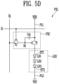
- the first transistor T1 may be connected between the first power supply VDD and the light source unit LSU.
- a first electrode (e.g., a source electrode) of the first transistor T1 may be connected to the first power supply VDD through the fifth transistor T5 and the first power line PL1
- a second electrode (e.g., a drain electrode) of the first transistor T1 may be connected via the sixth transistor T6 to the electrode of the light source unit LSU (e.g., the first contact electrode and/or the first pixel electrode of the corresponding pixel PXL).
- a gate electrode of the first transistor T1 is connected to a first node N1.
- the first transistor T1 may control driving current to be supplied to the light source unit LSU in response to the voltage of the first node N1.
- the second transistor T2 is connected between the data line Dj and the first electrode of the first transistor T1.
- a gate electrode of the second transistor T2 is connected to the corresponding scan line Si.
- the second transistor T2 may be turned on to electrically connect the data line Dj to the first electrode of the first transistor T1.
- a data signal supplied from the data line Dj may be transmitted to the first transistor T1.
- the third transistor T3 is connected between the other electrode of the first transistor T1 and the first node N1.
- a gate electrode of the third transistor T3 is connected to the corresponding scan line Si.
- the third transistor T3 may be turned on to electrically connect the first transistor T1 in the form of a diode.
- the fourth transistor T4 may be connected between the first node N1 and the initialization power supply Vint.
- a gate electrode of the fourth transistor T4 is connected to a preceding scan line, e.g., an i-1-th scan line Si-1.
- the fourth transistor T4 may be turned on so that the voltage of the initialization power supply Vint may be transmitted to the first node N1.
- the voltage of the initialization power supply Vint for initializing the gate voltage of the first transistor T1 may be less than or equal to the lowest voltage of the data signal.
- the sixth transistor T6 is connected between the first transistor T1 and the light source unit LSU.
- a gate electrode of the sixth transistor T6 is connected to a corresponding emission control line, e.g., the i-th emission control line Ei.
- the sixth transistor T6 may be turned off when an emission control signal having a gate-off voltage is supplied to the emission control line Ei, and may be turned on in other cases.
- light emitting element LD or "light emitting elements LD” will be used to arbitrarily designate at least one light emitting element of the first, second, and the third light emitting elements LD1, LD2, and LD3 or collectively designate the first, second, and third light emitting elements LD1, LD2, and LD3.
- the P-type end of the first light emitting element LD1 may be connected to the first power supply VDD through the first electrode ET1 of the light source unit LSU.
- the N-type end of the first light emitting element LD1 may be connected to the P-type end of the second light emitting element LD2.
- the P-type end of the second light emitting element LD2 may be connected to the N-type end of the first light emitting element LD1.
- the N-type end of the second light emitting element LD2 may be connected to the P-type end of the third light emitting element LD3.
- the P-type end of the third light emitting element LD3 may be connected to the N-type end of the second light emitting element LD2.
- the voltage to be applied between the first and second electrodes ET1 and ET2 may be increased, and the amount of driving current flowing to the light source unit LSU may be reduced, compared to a light source unit LSU having a structure in which light emitting elements LD are connected in parallel. Therefore, in the case where the light source unit LSU of each pixel PXL is formed of a serial structure, panel current flowing through the display panel PNL may be reduced as the display device is driven. Hence, power consumption may be reduced.
- the foregoing serial connection structure may be effectively used in reducing panel current in a large display panel PNL in which the panel current is comparatively large.
- each serial stage of the light source unit LSU includes a plurality of light emitting elements LD connected in parallel to each other.
- the light source unit LSU may include a plurality of first light emitting elements LD1 disposed in a first stage (also referred to as “first serial stage” or “first row”), and a plurality of second light emitting elements LD2 disposed in a second stage (also referred to as “second serial stage” or “second row”) subsequent to the first stage. Furthermore, the light source unit LSU may selectively further include at least one serial stage subsequent to the second stage. For example, the light source unit LSU may further include a plurality of third light emitting elements LD3 disposed in a third stage (referred to as "third serial stage” or “third row”) subsequent to the second stage. Furthermore, in an embodiment, at least one serial stage may further include at least one reverse light emitting element LDrv, but the present disclosure is not limited thereto.
- the first light emitting elements LD1 are connected in parallel to each other between first and second electrodes ET11 and ET21 of the first stage.
- the second light emitting elements LD2 are connected in parallel to each other between first and second electrodes ET12 and ET22 of the second stage.
- the third light emitting elements LD3 may be connected in parallel to each other between first and second electrodes ET13 and ET23 of the third stage.
- first and second electrodes ET11 to ET13 and ET21 to ET23 disposed in each serial stage may form split electrodes which are dispersed and disposed in the light source unit LSU.
- first electrode ET1 also referred to as “first split electrode”
- first split electrode will be used to arbitrarily designate at least one first electrode among the first electrodes ET11 to ET13 (also referred to as “first split electrodes") disposed in each serial stage, or collectively designate the first electrodes ET11 to ET13 disposed in each serial stage.
- second electrode ET2 (also referred to as “second split electrode”) will be used to arbitrarily designate at least one second electrode among the second electrodes ET21 to ET23 (also referred to as “second split electrodes”) disposed in each serial stage, or collectively designate the second electrodes ET21 to ET23 disposed in each serial stage.
- driving current/voltage conditions may be easily controlled to correspond to specifications of a desired product.
- the light source unit LSU in which the light emitting elements LD are connected in the serial/parallel combination structure makes it possible to reduce driving current compared to that of the light source unit LSU having a structure in which all of the light emitting elements LD are connected in parallel to each other as shown in the embodiments of FIGS.
- the pixel PXL in accordance with an embodiment of the present disclosure may include a pixel circuit PXC and/or a light source unit LSU which may have various structures.
- the structure of the pixel PXL which may be applied to the present disclosure is not limited to the embodiments illustrated in FIGS. 5A to 5E , and each pixel PXL may have various well-known structures.
- the pixel circuit PXC included in each pixel PXL may be formed of a well-known pixel circuit which may have various structures and/or be operated by various driving schemes.
- each pixel PXL may be configured in a passive light emitting display device, or the like.
- the pixel circuit PXC may be omitted, and each of the first and second electrodes ET1 and ET2 of the light source unit LSU may be directly connected to the scan line Si, the data line Dj, a power line, and/or a control line.
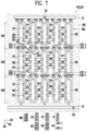
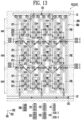
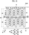
- FIGS. 6 and 7 are plan views each illustrating a pixel PXL in accordance with an embodiment of the present disclosure.
- Each pixel PXL illustrated in FIGS. 6 and 7 may be a pixel PXL in accordance with the embodiment of FIG. 5E .
- the pixels PXL disposed in the display area (DA of FIG. 4 ) may have substantially identical or similar structures.
- FIGS. 6 and 7 illustrate the structure of the pixel PXL, centered on the light source unit LSU of the pixel PXL in accordance with each embodiment.
- the pixel PXL may further include a circuit element (e.g., at least one circuit element that forms the pixel circuit PXC of FIGS. 5A to 5E ) for controlling each light source unit LSU.
- the circuit element may be disposed on a layer different from that of the light source unit LSU.
- the circuit element may be disposed in a pixel circuit layer located on one surface of the base layer BSL, and the light source unit LSU may be disposed in a display element layer disposed on the pixel circuit layer.
- FIGS. 6 and 7 illustrate an embodiment in which each light source unit LSU is connected, through first and second contact holes CH1 and CH2, to a predetermined power line (e.g., first and/or second power lines PL1 and/or PL2), a circuit element (e.g., at least one circuit element that forms the pixel circuit PXC), and/or a signal line (e.g., a scan line Si and/or a data line Dj), but the present disclosure is not limited thereto.
- a predetermined power line e.g., first and/or second power lines PL1 and/or PL2
- a circuit element e.g., at least one circuit element that forms the pixel circuit PXC
- a signal line e.g., a scan line Si and/or a data line Dj
- At least one of the first and second electrodes ET1 and ET2 of each pixel PXL may be directly connected to a predetermined power line and/or signal line without using, e.g., a contact hole and/or an intermediate line.
- the pixel PXL in accordance with an embodiment of the present disclosure may include a plurality of first electrodes ET1 and a plurality of second electrodes ET2 which are separated from each other and dispersed in the emission area EMA, and a plurality of light emitting elements LD connected in a serial/parallel combination structure between the first and second electrodes ET1 and ET2.
- the emission area EMA of each pixel PXL may refer to an area where the light emitting elements LD that form the light source unit LSU of the pixel PXL are disposed. Not only the light emitting elements LD but also the first and second electrodes ET1 and ET2 connected to the light emitting elements LD may be disposed in the emission area EMA.
- the emission area EMA may be enclosed by a light shielding and/or reflective bank (also referred to as "pixel defining layer") BNK.
- a light shielding and/or reflective bank also referred to as "pixel defining layer” BNK.
- the emission area EMA of each pixel PXL may be defined and/or sectioned by the bank BNK.
- the bank BNK may be disposed to enclose each emission area EMA.
- the bank BNK may be disposed between the emission areas EMA of the pixels PXL such that the bank BNK is disposed in a peripheral area of each pixel PXL and/or an area between adjacent pixels PXL.
- the first and second electrodes ET1 and ET2 may be dispersed in the emission area EMA in the form of a matrix in a first direction (e.g., a column direction or a vertical direction) DR1 and a second direction (e.g., a row direction or a horizontal direction) DR2.
- a first direction e.g., a column direction or a vertical direction
- a second direction e.g., a row direction or a horizontal direction
- an area where the first and second electrodes ET1 and ET2 and the light emitting elements LD of each serial stage are disposed may be defined as a sub-area with regard to the first direction DR1.
- the emission area EMA in which the light source unit LSU is disposed may be sectioned into the three sub-areas with regard to the first direction DR1.
- the emission area EMA may include a first sub-area SAR1, a second sub-area SAR2, and a third sub-area SAR3 which are successively disposed in the first direction DR1.
- At least one pair of first-stage first and second electrodes ET11 and ET21, and a plurality of first light emitting elements LD1 connected therebetween may be disposed in the first sub-area SAR1.
- a plurality of first-stage first electrodes ET11 and a plurality of first-stage second electrodes ET21 may be disposed in the first sub-area SAR1.
- at least one pair of first-stage first and second contact electrodes CE11 and CE21 that respectively correspond to the first and second electrodes ET11 and ET21 of the first stage may be selectively further disposed in the first sub-area SAR1.
- the first and second electrodes ET11 and ET21 of the first stage may be disposed at positions spaced apart from each other in the first sub-area SAR1.
- the first and second electrodes ET11 and ET21 of the first stage may be regularly arranged in the first sub-area SAR1, but the present disclosure is not limited thereto.
- the first and second electrodes ET11 and ET21 of the first stage each may have a bar shape extending in one direction in the first sub-area SAR1.
- the first and second electrodes ET11 and ET21 of the first stage each may have a bar shape extending in the first direction DR1 and be successively or alternately disposed at positions spaced apart from each other in the second direction DR2 intersecting with the first direction DR1.
- the shapes, the orientations, and/or the relative disposition structure of the first and second electrodes ET11 and ET21 of the first stage are not limited thereto and may be changed in various ways.
- the first and second electrodes ET11 and ET21 of the first stage may be disposed at positions spaced apart from each other in a bihelical structure or the like.
- each first-stage first electrode ET11 may be integrally or non-integrally connected to a first line (also referred to as "first connection line” or “first connection pattern") LI1.
- each pixel PXL may further include a first line LI1 connected to at least one first-stage first electrode ET11.
- each pixel PXL may further include a first line LI1 integrally connected to a plurality of first-stage first electrodes ET11.
- the first-stage first electrodes ET11 and the first line LI1 may be regarded as different areas of one electrode, line, or pattern.
- the width of the conductive pattern that forms the first-stage first electrodes ET11 and the first line LI1 may be partially reduced. If the foregoing structure is used, any one first-stage first electrode ET11 may be easily separated from the first line LI1, as needed. For example, in the case where a short-circuit defect is caused in at least one first light emitting element LD1 connected to any one first-stage first electrode ET11, the any one first-stage first electrode ET11 may be separated from the first line LI1 to allow the defect of the pixel PXL attributable to the short-circuit defect to be repaired.
- the width of each first-stage first electrode ET11 may remain constant to an area in which the first-stage first electrode ET11 is connected to the first line LI1.
- the first line LI1 may be supplied with a voltage of the first power supply VDD (a first power voltage) or a first driving signal (e.g., a scan signal, a data signal, or a predetermined other control signal) during a period in which the display device is operated.
- the first line LI1 may be electrically connected to a first contact hole CH1, a predetermined circuit element (e.g., at least one transistor that forms the pixel circuit PXC), a power line (e.g., the first power line PL1), and/or a signal line (e.g., the scan line Si, the data line Dj, or a predetermined control line).
- the first line LI1 may be electrically connected to a predetermined circuit element disposed thereunder through the first contact hole CH1, and be connected to the first power line PL1 through the circuit element.
- the first line LI1 may be connected, via the first contact hole CH1, etc., to a signal line to which a predetermined first driving signal is supplied.
- the first line LI1 may be directly connected to the first power line PL1 or a predetermined signal line without using the first contact hole CH1, and/or the circuit element.
- the first line LI1 may be integrally or non-integrally connected to the first power line PL1 or the predetermined signal line.
- the first line LI1 connected to the first-stage first electrodes ET11 of each of the pixels PXL may be first fabricated to be connected in common to a plurality of pixels PXL and be supplied with a first alignment signal (or a first alignment voltage) at the step of aligning the light emitting elements LD. Thereafter, the first line LI1 between the pixels PXL may be disconnected (or opened), so that the pixels PXL can be fabricated to be individually operable.
- each first-stage second electrode ET21 may have a separate individual pattern shape. Each first-stage second electrode ET21 may be electrically connected to at least one electrode of a subsequent stage. For example, each first-stage second electrode ET21 may be electrically connected to any one second-stage first electrode ET12 and/or any one second-stage first contact electrode CE12 through the corresponding first-stage second contact electrode CE21 or without using the first-stage second contact electrode CE21.
- a plurality of first light emitting elements LD1 may be disposed between the first and second electrodes ET11 and ET21 of the first stage.
- a plurality of first light emitting elements LD1 may be arranged in parallel to each other between each first-stage first electrode ET11 and the corresponding first-stage second electrode ET21.
- Each first light emitting element LD1 may include a first end EP1 connected to any one first-stage first electrode ET11, and a second end EP2 connected to any one first-stage second electrode ET21.
- the first end EP1 may be a P-type end
- the second end EP2 may be an N-type end.
- each first light emitting element LD1 may be connected in the forward direction between first and second electrodes ET11 and ET21 of the first stage.
- the first end EP1 of each of the first light emitting elements LD1 may be directly connected to any one first-stage first electrode ET11, or may be connected to the any one first-stage first electrode ET11 through any one first-stage first contact electrode CE11.
- the second end EP2 of each of the first light emitting elements LD1 may be directly connected to any one first-stage second electrode ET21, or may be connected to the any one first-stage second electrode ET21 through any one first-stage second contact electrode CE21.
- the first light emitting elements LD1 may form valid light sources of the first stage.
- At least one reverse light emitting element LDrv connected in a direction opposite to that of the first light emitting elements LD1 may be further connected between the first and second electrodes ET11 and ET21 of the first stage.
- the at least one reverse light emitting element LDrv may remain disabled in the pixel PXL.
- each first-stage first contact electrode CE11 may be disposed on each corresponding first-stage first electrode ET11.
- Each first-stage second contact electrode CE21 may be disposed on each corresponding first-stage second electrode ET21.
- a plurality of first-stage first contact electrodes CE11 disposed on each first-stage first electrode ET11, and a plurality of first-stage second contact electrodes CE21 disposed on each first-stage second electrode ET21 may be disposed in the first sub-area SAR1.
- the first and second contact electrodes CE11 and CE21 of the first stage may be successively or alternately disposed at positions spaced apart from each other in the second direction DR2 in the first sub-area SAR1.
- Each first-stage first contact electrode CE11 may be disposed on each corresponding first-stage first electrode ET11 and the first end EP1 of at least one first light emitting element LD1 adjacent to the first-stage first electrode ET11, and electrically connect the first end EP1 to the corresponding first-stage first electrode ET11.
- each first-stage second contact electrode CE21 may be disposed on each corresponding first-stage second electrode ET21 and the second end EP2 of at least one first light emitting element LD1 adjacent to the first-stage second electrode ET21, and electrically connect the second end EP2 to the corresponding first-stage second electrode ET21.
- the first and second contact electrodes CE11 and CE21 of the first stage may electrically connect the first light emitting elements LD1 between the first and second electrodes ET11 and ET21 of the first stage.
- each first-stage first contact electrode CE11 may have a separate individual pattern shape.
- Each first-stage second contact electrode CE21 may be integrally or non-integrally connected with at least one second-stage first contact electrode CE12.
- at least one 1-2-th stage connection electrode SCE1-2 configured to connect each first-stage second contact electrode CE21 to at least one second-stage first contact electrode CE12 of a subsequent stage may be disposed in a boundary area between the first sub-area SAR1 and the second sub-area SAR2.
- connection electrode SCE e.g., at least one first-stage second contact electrode CE21, at least one second-stage first contact electrode CE12, and the 1-2-th stage connection electrode SCE1-2
- connection electrode SCE e.g., at least one first-stage second contact electrode CE21, at least one second-stage first contact electrode CE12, and the 1-2-th stage connection electrode SCE1-2
- At least one pair of second-stage first and second electrodes ET12 and ET22, and a plurality of second light emitting elements LD2 connected therebetween may be disposed in the second sub-area SAR2.
- a plurality of second-stage first electrodes ET12 and a plurality of second-stage second electrodes ET22 may be disposed in the second sub-area SAR2.
- at least one pair of second-stage first and second contact electrodes CE12 and CE22 that respectively correspond to the first and second electrodes ET12 and ET22 of the second stage may be selectively further disposed in the second sub-area SAR2.
- the first and second electrodes ET12 and ET22 of the second stage may be disposed at positions spaced apart from each other in the second sub-area SAR2.
- the first and second electrodes ET12 and ET22 of the second stage may be regularly arranged in the second sub-area SAR2, but the present disclosure is not limited thereto.
- the first and second electrodes ET12 and ET22 of the second stage each may have a bar shape extending in one direction in the second sub-area SAR2.
- the first and second electrodes ET12 and ET22 of the second stage each may have a bar shape extending in the first direction DR1 and be successively and/or alternately disposed at positions spaced apart from each other in the second direction DR2 intersecting with the first direction DR1.
- the shapes, the orientations, and/or the relative disposition structure of the first and second electrodes ET12 and ET22 of the second stage may be changed in various ways.
- each of the first and second electrodes ET12 and ET22 of the second stage that is an intermediate stage of the serial structure may have a separate individual pattern shape.
- Each of the first and second electrodes ET12 and ET22 of the second stage is connected to at least one electrode of a preceding stage (i.e., the first stage) or a subsequent stage (i.e., the third stage).
- each second-stage first electrode ET12 may be electrically connected to any one first-stage (i.e., preceding-stage) second electrode ET21 and/or any one first-stage second contact electrode CE21 through the corresponding second-stage first contact electrode CE12 or without using the second-stage first contact electrode CE12.
- Each second-stage second electrode ET22 may be electrically connected to any one third-stage (i.e., subsequent-stage) first electrode ET13 and/or any one third-stage first contact electrode CE13 through the corresponding second-stage second contact electrode CE22 or without using the second-stage second contact electrode CE22.
- each second-stage first electrode ET12 may have a separate individual pattern shape, and each second-stage second electrode ET22 may be directly connected to the second line LI2 to which a power voltage (e.g., a voltage of the second power supply VSS (a second power voltage)) and/or signal (e.g., second driving signal) different from that of the first line LI1 is supplied.
- a power voltage e.g., a voltage of the second power supply VSS (a second power voltage)
- signal e.g., second driving signal
- a plurality of second light emitting elements LD2 are disposed between the first and second electrodes ET12 and ET22 of the second stage.
- the plurality of second light emitting elements LD2 are arranged in parallel to each other between each second-stage first electrode ET12 and the corresponding second-stage second electrode ET22.
- Each second light emitting element LD2 may include a first end EP1 connected to any one second-stage first electrode ET12, and a second end EP2 connected to any one second-stage second electrode ET22.
- the first end EP1 may be a P-type end
- the second end EP2 may be an N-type end.
- each second light emitting element LD2 may be connected in the forward direction between the first and second electrodes ET12 and ET22 of the second stage.
- the first end EP1 of each of the second light emitting elements LD2 may be directly connected to any one second-stage first electrode ET12, or may be connected to the any one second-stage first electrode ET12 through any one second-stage first contact electrode CE12.
- the second end EP2 of each of the second light emitting elements LD2 may be directly connected to any one second-stage second electrode ET22, or may be connected to the any one second-stage second electrode ET22 through any one second-stage second contact electrode CE22.
- the second light emitting elements LD2 may form valid light sources of the second stage.
- At least one reverse light emitting element LDrv connected in a direction opposite to that of the second light emitting elements LD2 may be further connected between the first and second electrodes ET12 and ET22 of the second stage.
- the at least one reverse light emitting element LDrv may remain disabled in the pixel PXL.
- each second-stage first contact electrode CE12 is disposed on each corresponding second-stage first electrode ET12.
- Each second-stage second contact electrode CE22 is disposed on each corresponding second-stage second electrode ET22.
- a plurality of second-stage first contact electrodes CE12 disposed on each second-stage first electrode ET12, and a plurality of second-stage second contact electrodes CE22 disposed on each second-stage second electrode ET22 may be disposed in the second sub-area SAR2.
- the first and second contact electrodes CE12 and CE22 of the second stage may be successively or alternately disposed at positions spaced apart from each other in the second direction DR2 in the second sub-area SAR2.
- Each second-stage first contact electrode CE12 may be disposed on each corresponding second-stage first electrode ET12 and the first end EP1 of at least one second light emitting element LD2 adjacent to the second-stage first electrode ET12, and electrically connect the first end EP1 to the corresponding second-stage first electrode ET12.
- each second-stage second contact electrode CE22 may be disposed on each corresponding second-stage second electrode ET22 and the second end EP2 of at least one second light emitting element LD2 adjacent to the second-stage second electrode ET22, and electrically connect the second end EP2 to the corresponding second-stage second electrode ET22.
- the first and second contact electrodes CE12 and CE22 of the second stage may electrically connect the second light emitting elements LD2 between the first and second electrodes ET12 and ET22 of the second stage.
- each second-stage first contact electrode CE12 may be integrally or non-integrally connected with at least one first-stage (i.e., preceding-stage) second contact electrode CE21.
- Each second-stage second contact electrode CE22 may be integrally or non-integrally connected with at least one third-stage (i.e., subsequent-stage) first contact electrode CE13.
- at least one 1-2-th stage connection electrode SCE1-2 configured to connect at least one first-stage second contact electrode CE21 and at least one second-stage first contact electrode CE12 may be disposed in a boundary area between the first sub-area SAR1 and the second sub-area SAR2.
- At least one 2-3-th stage connection electrode SCE2-3 configured to connect at least one second-stage second contact electrode CE22 and at least one third-stage first contact electrode CE13 may be disposed in a boundary area between the second sub-area SAR2 and the third sub-area SAR3.
- each second-stage second contact electrode CE22 may have a separate individual pattern shape. In this case, each second-stage second contact electrode CE22 may be connected to the second line LI2 through the second-stage second electrode ET22.
- At least one pair of third-stage first and second electrodes ET13 and ET23, and a plurality of third light emitting elements LD3 connected therebetween may be disposed in the third sub-area SAR3.
- a plurality of third-stage first electrodes ET13 and a plurality of third-stage second electrodes ET23 may be disposed in the third sub-area SAR3.
- at least one pair of third-stage first and second contact electrodes CE13 and CE23 that respectively correspond to the first and second electrodes ET13 and ET23 of the third stage may be selectively further disposed in the third sub-area SAR3.
- the first and second electrodes ET13 and ET23 of the third stage may be disposed at positions spaced apart from each other in the third sub-area SAR3.
- the first and second electrodes ET13 and ET23 of the third stage may be regularly arranged in the third sub-area SAR3, but the present disclosure is not limited thereto.
- the first and second electrodes ET13 and ET23 of the third stage each may have a bar shape extending in one direction in the third sub-area SAR3.
- the first and second electrodes ET13 and ET23 of the third stage each may have a bar shape extending in the first direction DR1 and be successively or alternately disposed at positions spaced apart from each other in the second direction DR2 intersecting with the first direction DR1.
- the shapes, the orientations, and/or the relative disposition structure of the first and second electrodes ET13 and ET23 of the third stage may be changed in various ways.
- each third-stage first electrode ET13 may have a separate individual pattern shape. Each third-stage first electrode ET13 may be electrically connected to at least one electrode of a preceding stage. For example, each third-stage first electrode ET13 may be electrically connected to any one second-stage second electrode ET22 and/or any one second-stage second contact electrode CE22 through the corresponding third-stage first contact electrode CE13 or without using the third-stage first contact electrode CE13.
- each third-stage second electrode ET23 may be integrally or non-integrally connected to a second line (also referred to as "second connection line” or “second connection pattern") LI2.
- each pixel PXL may further include a second line LI2 connected to at least one third-stage second electrode ET23.
- each pixel PXL may further include a second line LI2 integrally connected to a plurality of third-stage second electrodes ET23.
- the third-stage second electrodes ET23 and the second line LI2 may be regarded as different areas of one electrode, line, or pattern.
- the width of the conductive pattern that forms the third-stage second electrodes ET23 and the second line LI2 may be partially reduced. If the foregoing structure is used, any one third-stage second electrode ET23 may be easily separated from the second line LI2, as needed. For example, in the case where a short-circuit defect is caused in at least one third light emitting element LD3 connected to any one third-stage second electrode ET23, the any one third-stage second electrode ET23 may be separated from the second line LI2 to allow the defect of the pixel PXL attributable to the short-circuit defect to be repaired. However, the present disclosure is not limited thereto. For example, in an embodiment, the width of each third-stage second electrode ET23 may remain constant to an area in which the third-stage second electrode ET23 is connected to the second line LI2.
- the second line LI2 may be supplied with the voltage of the second power supply VSS or a second driving signal (e.g., a scan signal, a data signal, or a predetermined other control signal) during a period in which the display device is operated.
- the second line LI2 may be electrically connected to a second contact hole CH2, a predetermined circuit element (e.g., at least one transistor that forms the pixel circuit PXC), a power line (e.g., the second power line PL2), and/or a signal line (e.g., the scan line Si, the data line Dj, or a predetermined control line).
- the second line LI2 may be connected, through the second contact hole CH2, to the second power line PL2 disposed thereunder.
- the second line LI2 may be directly connected to the second power line PL2 or a predetermined signal line without using, e.g., the second contact hole CH2, and/or the circuit element.
- the second line LI2 may be integrally or non-integrally connected to the second power line PL2 or the predetermined signal line.
- the second line LI2 connected to the second electrodes ET23 of the last stage of each of the pixels PXL may be connected in common to a plurality of pixels PXL.
- the second line LI2 may be supplied with a predetermined second alignment signal (or a second alignment voltage) at the step of aligning the light emitting elements LD.
- the second line LI2 may be supplied with the voltage of the second power supply VSS or a predetermined second driving signal.
- a plurality of third light emitting elements LD3 may be disposed between the first and second electrodes ET13 and ET23 of the third stage.
- a plurality of third light emitting elements LD3 may be arranged in parallel to each other between each third-stage first electrode ET13 and the corresponding third-stage second electrode ET23.
- Each third light emitting element LD3 may include a first end EP1 connected to any one third-stage first electrode ET13, and a second end EP2 connected to any one third-stage second electrode ET23.
- the first end EP1 may be a P-type end
- the second end EP2 may be an N-type end.
- each third light emitting element LD3 may be connected in the forward direction between the first and second electrodes ET13 and ET23 of the third stage.
- the first end EP1 of each of the third light emitting elements LD3 may be directly connected to any one third-stage first electrode ET13, or may be connected to the any one third-stage first electrode ET13 through any one third-stage first contact electrode CE13.
- the second end EP2 of each of the third light emitting elements LD3 may be directly connected to any one third-stage second electrode ET23, or may be connected to the any one third-stage second electrode ET23 through any one third-stage second contact electrode CE23.
- the third light emitting elements LD3 may form valid light sources of the third stage.
- At least one reverse light emitting element LDrv connected in a direction opposite to that of the third light emitting elements LD3 may be further connected between the first and second electrodes ET13 and ET23 of the third stage.
- the at least one reverse light emitting element LDrv may remain disabled in the pixel PXL.
- the pixel PXL may include at least one reverse light emitting element LDrv disposed in the emission area EMA, as well as including a plurality of light emitting elements LD, e.g., first, second, and/or third light emitting elements, LD1, LD2, and LD3, disposed in the emission area EMA to form valid light sources.
- the number of light emitting elements LD disposed in the emission area EMA may be greater than the number of reverse light emitting elements LDrv.
- each of the first, second, and third sub-areas SAR1, SAR2, and SAR3 may include first, second, and third light emitting elements LD1, LD2, and LD3 the number of which is greater than the number of reverse light emitting elements LDrv.
- the light emitting elements LD supplied to the emission area EMA may be controlled to be aligned and biased in any one direction (e.g., the forward direction) by adjusting alignment signals (or alignment voltages) to be applied to the respective alignment electrodes or forming a magnetic field.
- each of the light emitting elements LD disposed in the emission area EMA may be a light emitting element which is made of material having an inorganic crystal structure and has a subminiature size, e.g., ranging from the nanometer scale to the micrometer scale.
- each light emitting element LD may be a subminiature rod-type light emitting element having a size ranging from the nanometer scale to the micrometer scale, as illustrated in FIGS. 1A to 3B .
- the size, the type, the shape, etc. of the light emitting elements LD may be changed in various ways.
- FIG. 6 illustrates that, in the area where a pair of first and second electrodes ET1 and ET2 are disposed to face each other, each light emitting element LD is uniformly horizontally arranged in the first direction DR1 between the first and second electrodes ET1 and ET2, the present disclosure is not limited thereto.
- at least one of the light emitting elements LD may be arranged and/or connected in a diagonal direction between the first and second electrodes ET1 and ET2.
- FIG. 6 illustrates that, in the area where a pair of first and second electrodes ET1 and ET2 are disposed to face each other, each light emitting element LD is uniformly horizontally arranged in the first direction DR1 between the first and second electrodes ET1 and ET2, the present disclosure is not limited thereto.
- at least one of the light emitting elements LD may be arranged and/or connected in a diagonal direction between the first and second electrodes ET1 and ET2.
- FIG. 6 illustrates that, in the area where a pair of first and second electrodes ET1 and ET
- At least one light emitting element (e.g., an invalid light source other than a reverse light emitting element LDrv) that is not completely connected between the first and second electrodes ET1 and ET2 may be further disposed in each pixel area and/or an area provided around the pixel area.
- a light emitting element e.g., an invalid light source other than a reverse light emitting element LDrv
- the light emitting elements LD may be reliably disposed between the first and second electrodes ET1 and ET2. Thereafter, since the first and second contact electrodes CE1 and CE2 are formed on the opposite ends of the light emitting elements LD, e.g., on the first and second ends EP1 and EP2, the light emitting elements LD may be more reliably connected between the first and second electrodes ET1 and ET2.
- each third-stage first contact electrode CE13 may be disposed on each corresponding third-stage first electrode ET13.
- Each third-stage second contact electrode CE23 may be disposed on each corresponding third-stage second electrode ET23.
- a plurality of third-stage first electrodes ET13 and a plurality of third-stage second electrodes ET23 are disposed in the third sub-area SAR3
- a plurality of third-stage first contact electrodes CE13 disposed on each third-stage first electrode ET13, and a plurality of third-stage second contact electrodes CE23 disposed on each third-stage second electrode ET23 may be disposed in the third sub-area SAR3.
- the first and second contact electrodes CE13 and CE23 of the third stage may be successively or alternately disposed at positions spaced apart from each other in the second direction DR2 in the third sub-area SAR3.
- Each third-stage first contact electrode CE13 may be disposed on each corresponding third-stage first electrode ET13 and the first end EP1 of at least one third light emitting element LD3 adjacent to the third-stage first electrode ET13, and electrically connect the first end EP1 to the corresponding third-stage first electrode ET13.
- each third-stage second contact electrode CE23 may be disposed on each corresponding third-stage second electrode ET23 and the second end EP2 of at least one third light emitting element LD3 adjacent to the third-stage second electrode ET23, and electrically connect the second end EP2 to the corresponding third-stage second electrode ET23.
- the first and second contact electrodes CE13 and CE23 of the third stage may electrically connect the third light emitting elements LD3 between the first and second electrodes ET13 and ET23 of the third stage.
- each third-stage first contact electrode CE13 may be integrally or non-integrally connected with at least one second-stage (i.e., a preceding-stage) second contact electrode CE22.
- each third-stage first contact electrode CE13 may be integrally connected with at least one 2-3-th stage connection electrode SCE2-3 and at least one second-stage second contact electrode CE22 that are disposed in the boundary area between the second and third sub-areas SAR2 and SAR3.
- Each third-stage second contact electrode CE23 may have a separate individual pattern shape.
- the emission area EMA includes at least three sub-areas, as described above, in a K-th sub-area (K is a natural number of 3 or more) of the emission area EMA, there may be disposed the first and second electrodes of a K-th stage that are disposed at positions spaced apart from each other, K-th light emitting elements arranged in parallel to each other between the first and second electrodes of the K-th stage, the first and second contact electrodes of the K-th stage that are respectively disposed on the first and second electrodes of the K-th stage and configured to electrically connect the K-th light emitting elements between the first and second electrodes of the K-th stage.
- K is a natural number of 3 or more
- a boundary area between the K-th sub-area and a sub-area (i.e., a [K-1]-th sub-area) of a preceding stage there may be disposed at least one a [K-1]-K-th stage connection electrode configured to connect the first contact electrode of the K-th stage to the second contact electrode of the preceding stage (i.e., the [K-1]-th stage).
- the first electrode ET11 of the first stage may be connected to the first line LI1
- the second electrode of the K-th stage or the last stage may be connected to the second line LI2.
- each of the second electrode ET21 of the first stage, the first and second electrodes of intermediate stages including the second stage, and the first electrode of the K-th stage or the last stage may have a separate individual pattern shape.
- the pixel PXL may further include a plurality of first partition walls PW1 (also referred to as “first wall(s)” or “first bank(s)”) which overlap with each first electrode ET1, and a plurality of second partition walls PW2 (also referred to as “second wall(s)” or “second bank(s)”) which overlap with each second electrode ET2.
- first partition walls PW1 and the second partition walls PW2 each may have a separate individual pattern.
- first partition walls PW1 and the second partition walls PW2 may be respectively disposed under the first electrodes ET1 and the second electrodes ET2.
- each first partition wall PW1 may be disposed under any one first electrode ET1 disposed in any one sub-area of the first, second, and third sub-areas SAR1, SAR2, and SAR3.
- Each second partition wall PW2 may be disposed under any one second electrode ET2 disposed in any one sub-area of the first, second, and third sub-areas SAR1, SAR2, and SAR3.
- each first partition wall PW1 may have a width less than that of each first electrode ET1 and be disposed under the first electrode ET1.
- each first partition wall PW1 may have a shape corresponding to the first electrode ET1 and be disposed inside the first electrode ET1, in a plan view.
- the first electrodes ET1 may protrude upward in the area in which the first partition walls PW1 are disposed. Therefore, light emitted from the first ends EP1 of the light emitting elements LD that face the first electrodes ET1 may be controlled to more effectively travel in the frontal direction of the display device.
- each second partition wall PW2 may have a width less than that of each second electrode ET2 and be disposed under the second electrode ET2.
- each second partition wall PW2 may have a shape corresponding to each second electrode ET2 and be disposed inside the second electrode ET2, in a plan view.
- the second electrodes ET2 may protrude upward in the area in which the second partition walls PW2 are disposed. Therefore, light emitted from the second ends EP2 of the light emitting elements LD that face the second electrodes ET2 may be controlled to more effectively travel in the frontal direction of the display device.
- the emission area EMA of each pixel PXL is divided into a plurality of sub-areas in any one direction (e.g., the first direction DR1), and the first and second electrodes ET1 and ET2, the light emitting elements LD, and the first and second contact electrodes CE1 and CE2 are disposed in each sub-area.
- the second contact electrodes CE2 of any one stage may be connected to the first contact electrodes CE1 of a subsequent stage, between adjacent sub-areas, through the connection electrode SCE passing through the boundary area between the sub-areas.
- the light emitting elements LD supplied to each emission area EMA may be connected in a serial/parallel combination structure to form each light source unit LSU.
- each pixel PXL may be reliably driven, and a driving current that flows through the display panel PNL may be reduced. Hence, the power consumption efficiency may be improved.
- the light emitting elements LD are biased-aligned, a plurality of first and second electrodes ET1 and ET2 are separately disposed in a plurality of sub-areas, and the first and second contact electrodes CE1 and CE2 are alternately connected between the adjacent sub-areas. Hence, main alignment direction of the biased-aligned light emitting elements LD may match with the forward direction of each serial stage.
- the number of light emitting elements LD capable of being used as valid light sources to form each light source unit LSU among the light emitting elements supplied to the emission area EMA of each pixel PXL may be increased. That is, in accordance with the foregoing embodiments, the application efficiency of the light emitting elements LD can be enhanced.
- FIGS. 8 to 11 are sectional views each illustrating a pixel PXL in accordance with an embodiment of the present disclosure, and for example illustrate different embodiments of a cross-section of the pixel PXL corresponding to line I-I' of FIG. 7 .
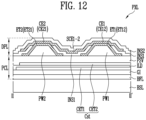
- FIG. 12 is a sectional view illustrating a pixel PXL in accordance with an embodiment of the present disclosure, and for example illustrates an embodiment of a cross-section of the pixel PXL corresponding to line II-II' of FIG. 7 .
- FIGS. 8 to 12 an embodiment of the cross-sectional structure of each pixel PXL will be described with reference to FIGS. 8 to 12 along with FIGS. 4 to 7 .
- the pixel PXL in accordance with an embodiment of the present disclosure may include a display element layer DPL disposed on one surface of the base layer BSL and including a plurality of light emitting elements LD. Furthermore, the pixel PXL may selectively include a pixel circuit layer PCL. For example, the pixel PXL may further include a pixel circuit layer PCL disposed between the base layer BSL and the display element layer DPL.
- the pixel circuit layer PCL may include a plurality of insulating layers disposed between respective electrodes and/or lines.
- the pixel circuit layer PCL may include a buffer layer BFL, a gate insulating layer GI, an interlayer insulating layer ILD, and a passivation layer PSV which are successively stacked on one surface of the base layer BSL.
- the pixel circuit layer PCL may further include at least one light shielding pattern (not shown) disposed under at least some transistors T.
- the buffer layer BFL may prevent impurities from diffusing into each circuit element.
- the buffer layer BFL may be formed of a single layer, or may be formed of multiple layers having at least two or more layers. In the case where the buffer layer BFL has a multilayer structure, the respective layers may be formed of the same material or different materials. In an embodiment, the buffer layer BFL may be omitted.
- each transistor T may include a semiconductor layer SCL, a gate electrode GE, and first and second transistor electrodes TE1 and TE2.
- FIGS. 8 to 11 illustrate an embodiment in which each transistor T includes the first and second transistor electrodes TE1 and TE2 that are formed separately from the semiconductor layer SCL, the present disclosure is not limited thereto.
- the first and/or second transistor electrode TE1 and/or TE2 provided in at least one transistor T disposed in each pixel area may be integrally formed with the corresponding semiconductor layer SCL.
- the semiconductor layer SCL may be disposed on the buffer layer BFL.
- the semiconductor layer SCL may be disposed between the gate insulating layer GI and the base layer BSL on which the buffer layer BFL is formed.
- the semiconductor layer SCL may include a first area which comes into contact with each first transistor electrode TE1, a second area which comes into contact with each second transistor electrode TE2, and a channel area disposed between the first and second areas.
- one of the first and second areas may be a source area, and the other may be a drain area.
- the semiconductor layer SCL may be a semiconductor pattern formed of polysilicon, amorphous silicon, an oxide semiconductor, etc.
- the channel area of the semiconductor layer SCL may be an intrinsic semiconductor, which is an undoped semiconductor pattern.
- Each of the first and second areas of the semiconductor layer SCL may be a semiconductor pattern doped with a predetermined impurity.
- the gate electrode GE may be disposed on the semiconductor layer SCL with the gate insulating layer GI interposed therebetween.
- the gate electrode GE may be disposed between the gate insulating layer GI and the interlayer insulating layer ILD and overlap at least one area of the semiconductor layer SCL.
- the first and second transistor electrodes TE1 and TE2 may be disposed on each semiconductor layer SCL with at least one interlayer insulating layer ILD interposed therebetween.
- the first and second transistor electrodes TE1 and TE2 may be disposed on respective different ends of the semiconductor layer SCL with the gate insulating layer GI and the interlayer insulating layer ILD interposed therebetween.
- the first and second transistor electrodes TE1 and TE2 may be electrically connected to each semiconductor layer SCL.
- the first and second transistor electrodes TE1 and TE2 may be connected to the first and second areas of the semiconductor layer SCL through corresponding contact holes which pass through the gate insulating layer GI and the interlayer insulating layer ILD.
- any one of the first and second transistor electrodes TE1 and TE2 may be a source electrode, and the other may be a drain electrode.
- At least one transistor T provided in the pixel circuit PXC may be connected to at least one pixel electrode.
- any one (e.g., the drain electrode) of the first and second transistor electrodes TE1 and TE2 of the first transistor T1 illustrated in FIG. 5E may be electrically connected to the first-stage first electrodes ET11 of the corresponding pixel PXL both through a contact hole (e.g., the first contact hole CH1) passing through the passivation layer PSV and through the first line LI1 provided over the passivation layer PSV.
- the storage capacitor Cst may include a first capacitor electrode CET1 and a second capacitor electrode CET2 which are disposed on different layers and overlap with each other.
- the first capacitor electrode CET1 may be disposed on the same layer as that of the gate electrode GE of the transistor T.
- the second capacitor electrode CET2 may be disposed on the same layer as that of the first and second transistor electrodes TE1 and TE2 of the transistor T.
- the present disclosure is not limited thereto.
- the positions of the first capacitor electrode CET1 and/or the second capacitor electrode CET2 may be changed in various ways.
- the interlayer insulating layer ILD may be formed of a plurality of insulating layers, and the first or second capacitor electrode CET1 or CET2 may be disposed between the plurality of insulating layers.
- at least one of the first and second capacitor electrodes CET1 and CET2 may be formed of a plurality conductive layers.
- At least one signal line and/or power line that is connected to each pixel PXL may be disposed on a layer identical with that of an electrode of the transistors T of the circuit elements that form the pixel circuit PXC.
- the scan line Si of each pixel PXL may be disposed on the same layer as that of the gate electrodes GE.
- the data line Dj of each pixel PXL may be disposed on the same layer as that of the first and second transistor electrodes TE1 and TE2 of the transistors T.
- the first and/or second power lines PL1 and PL2 may be disposed on the same layer as that of the gate electrodes GE or the first and second transistor electrodes TE1 and TE2 of the transistors T.
- the display element layer DPL includes a light source unit LSU of each of the pixels PXL.
- the display element layer DPL may include a plurality of first and second electrodes ET1 and ET2 disposed in the emission area EMA of each pixel PXL, a plurality of light emitting elements LD disposed between the first and second electrodes ET1 and ET2, and a plurality of first and second contact electrodes CE1 and CE2 provided to electrically connect the light emitting elements LD between the first and second electrodes ET1 and ET2.
- the display element layer DPL may further include, e.g., at least one conductive layer and/or insulating layer.
- the display element layer DPL may include first and second partition walls PW1 and PW2, first and second electrodes ET1 and ET2, a first insulating layer INS1, light emitting elements LD, an insulating pattern INP, first and second contact electrodes CE1 and CE2, and a second insulating layer INS2, which are successively disposed and/or formed over the base layer BSL and/or the pixel circuit layer PCL.
- the first and second partition walls PW1 and PW2 may be disposed at positions spaced apart from each other in the emission area EMA of each pixel PXL.
- the first and second partition walls PW1 and PW2 may protrude from the base layer BSL and/or the pixel circuit layer PCL in a height direction of the base layer BSL.
- the first and second partition walls PW1 and PW2 may have substantially the same height, but the present disclosure is not limited thereto.
- the first partition wall PW1 may be disposed between the base layer BSL and/or the pixel circuit layer PCL and each first electrode ET1.
- the first partition walls PW1 may be disposed adjacent to the first ends EP1 of the light emitting elements LD.
- one side surface of each of the first partition walls PW1 may be positioned adjacent to the first ends EP1 of the light emitting elements LD and disposed to face the first ends EP1.
- the one side surface of the first partition wall PW1 may be disposed to face the second end EP2 of the reverse light emitting element LDrv.
- the second partition wall PW2 may be disposed between the base layer BSL and/or the pixel circuit layer PCL and the second electrode ET2.
- the second partition wall PW2 may be disposed adjacent to the second ends EP2 of the light emitting elements LD.
- one side surface of the second partition wall PW2 may be positioned adjacent to the second ends EP2 of the light emitting elements LD and disposed to face the second ends EP2.
- the one side surface of the second partition wall PW2 may be disposed to face the first end EP1 of the reverse light emitting element LDrv.
- each of the first and second partition walls PW1 and PW2 may have various shapes.
- the first and second partition walls PW1 and PW2 may have a trapezoidal cross-section the width of which is gradually reduced upward.
- each of the first and second partition walls PW1 and PW2 may have an inclined surface on at least one side.
- the first and second partition walls PW1 and PW2 may have a semi-circular or semi-elliptical cross-section the width of which is gradually reduced upward.
- each of the first and second partition walls PW1 and PW2 may have a curved surface on at least one side surface.
- At least one electrode and/or insulating layer disposed over the first and second partition walls PW1 and PW2 may have a curved surface in an area corresponding to the first and second partitions PW1 and PW2.
- each of the first and second partition walls PW1 and PW2 may be changed in various ways rather than being particularly limited.
- at least one of the first and second partition walls PW1 and PW2 may be omitted or changed in position.
- Each of the first and second partition walls PW1 and PW2 may include insulating material having at least one inorganic material and/or organic material.
- the first and second partition walls PW1 and PW2 may include at least one inorganic layer including various known inorganic insulating materials such as silicon nitride (SiNx) or silicon oxide (SiOx).
- the first and second partition walls PW1 and PW2 may include at least one organic layer and/or photoresist layer containing various kinds of known organic insulating materials, or may form a single- or multi-layer insulator containing organic/inorganic materials in combination.
- the constituent materials of the first and second partition walls PW1 and PW2 may be changed in various ways.
- each of the first and second partition walls PW1 and PW2 may function as a reflector.
- the first and second partition walls PW1 and PW2 along with the first and second electrodes ET1 and ET2 provided on the first and second partition walls PW1 and PW2 may function as reflectors that guide light emitted from each light emitting element LD in a desired direction, thus enhancing the light efficiency of the pixel PXL.
- the first and second electrodes ET1 and ET2 may be respectively disposed over the first and second partition walls PW1 and PW2.
- the first and second electrodes ET1 and ET2 may be disposed at positions spaced apart from each other in each pixel area (particularly, each emission area EMA).
- the first and second electrodes ET1 and ET2 that are respectively disposed over the first and second partition walls PW1 and PW2 may have shapes corresponding to the respective shapes of the first and second partition walls PW1 and PW2.
- the first and second electrodes ET1 and ET2 may have inclined surfaces or curved surfaces corresponding to the first and second partition walls PW1 and PW2, respectively, and protrude in the height direction of the base layer BSL.
- each of the first and second electrodes ET1 and ET2 includes at least one conductive material.
- each of the first and second electrodes ET1 and ET2 may include at least one material among at least one metal of various metal materials including silver (Ag), magnesium (Mg), aluminium (Al), platinum (Pt), palladium (Pd), gold (Au), nickel (Ni), neodymium (Nd), iridium (Ir), chromium (Cr), titanium (Ti), molybdenum (Mo), copper (Cu), etc., or an alloy thereof, conductive oxide such as indium tin oxide (ITO), indium zinc oxide (IZO), zinc oxide (ZnO), antimony zinc oxide (AZO), indium tin zinc oxide (ITZO), tin oxide (SnO2), and a conductive polymer such as PEDOT, but the present disclosure is not limited thereto.
- each of the first and second electrodes ET1 and ET2 may include other conductive materials such as a carbon nanotube and graphene.
- each of the first and second electrodes ET1 and ET2 may include at least one of various conductive materials to have conductivity, and the constituent material thereof is not particularly limited.
- each of the first and second electrodes ET1 and ET2 may have the same conductive material, or at least one different conductive material.
- Each of the first and second electrodes ET1 and ET2 may have a single-layer or multilayer structure.
- each of the first and second electrodes ET1 and ET2 may include at least one reflective electrode layer.
- Each of the first and second electrodes ET1 and ET2 may selectively further include at least one of at least one transparent electrode layer disposed over and/or under the reflective electrode layer, and at least one conductive capping layer covering an upper portion of the reflective electrode layer and/or the transparent electrode layer.
- the reflective electrode layer of each of the first and second electrodes ET1 and ET2 may be formed of conductive material having a uniform reflectivity.
- the reflective electrode layer may include at least one of various metal materials including silver (Ag), magnesium (Mg), aluminium (Al), platinum (Pt), palladium (Pd), gold (Au), nickel (Ni), neodymium (Nd), iridium (Ir), chromium (Cr), titanium (Ti), molybdenum (Mo), copper (Cu), etc., or an alloy thereof., but the present disclosure is not limited thereto.
- the reflective electrode layer may be formed of various reflective conductive materials.
- Each of the first and second electrodes ET1 and ET2 that includes the reflective electrode layer may enable light emitted from the opposite ends of each of the light emitting elements LD, i.e., the first and second ends EP1 and EP2, to travel in a direction (e.g., in a frontal direction) in which an image is displayed.
- first and second electrodes ET1 and ET2 respectively have inclined or curved surfaces corresponding to the shapes of the first and second partition walls PW1 and PW2 and are respectively disposed to face the first and second ends EP1 and EP2 of the light emitting elements LD, light emitted from the first and second ends EP1 and EP2 of each of the light emitting elements LD may be reflected by the first and second electrodes ET1 and ET2 and thus more reliably travel in the frontal direction of the display panel PNL (e.g., in an upward direction of the base layer BSL). Thereby, the efficiency of light emitted from the light emitting elements LD may be enhanced.
- each of the first and second electrodes ET1 and ET2 may be formed of various transparent conductive materials.
- the transparent electrode layer may include ITO, IZO or ITZO, but the present disclosure is not limited thereto.
- each of the first and second electrodes ET1 and ET2 may have a triple-layer structure having a stacked structure of ITO/Ag/ITO. As such, if the first and second electrodes ET1 and ET2 each are formed of a multilayer structure including at least two or more layers, voltage drop due to signal delay (RC delay) may be minimized. Thus, a desired voltage can be effectively transmitted to the light emitting elements LD.
- RC delay signal delay
- each of the first and second electrodes ET1 and ET2 includes the conductive capping layer covering the reflective electrode layer and/or the transparent electrode layer, it is possible to prevent the reflective electrode layer of the first and second electrodes ET1 and ET2 from being damaged due to defects caused during the manufacturing process of the pixel PXL.
- the conductive capping layer may be selectively included in the first and second electrodes ET1 and ET2, and may be omitted depending on embodiments.
- the conductive capping layer may be considered as a component of each of the first and second electrodes ET1 and ET2, or considered as a separate component disposed on the first and second electrodes ET1 and ET2.
- the first insulating layer INS1 may be disposed on predetermined areas of the first and second electrodes ET1 and ET2.
- the first insulating layer INS1 may be formed to cover predetermined areas of the first and second electrodes ET1 and ET2, and may include an opening to expose other predetermined areas of the first and second electrodes ET1 and ET2.
- the first insulating layer INS1 may expose the first and second electrodes ET1 and ET2 in predetermined first and second contact portions CNT1 and CNT2.
- the first insulating layer INS1 may be omitted.
- the light emitting elements LD may be directly disposed on the passivation layer PSV and/or one end of each of the first and second electrodes ET1 and ET2.
- the first insulating layer INS1 may be primarily formed to cover the overall surfaces of the first and second electrodes ET1 and ET2. After the light emitting elements LD are supplied and aligned on the first insulating layer INS1, the first insulating layer INS1 may be partially opened to expose the first and second electrodes ET1 and ET2 in respective predetermined areas (e.g., the respective first and second contact portions CNT1 and CNT2) on the first and second partition walls PW1 and PW2.
- the first insulating layer INS1 may be patterned in the form of an individual pattern which is sectionally disposed under the light emitting elements LD after the supply and alignment of the light emitting elements LD have been completed.
- the first insulating layer INS1 may be interposed between the first and second electrodes ET1 and ET2 and the light emitting elements LD, and may expose at least one area of each of the first and second electrodes ET1 and ET2.
- the first insulating layer INS1 may be formed to cover the first and second electrodes ET1 and ET2, so that it is possible to prevent the first and second electrodes ET1 and ET2 from being damaged or to prevent metal from being precipitated in a subsequent process.
- the first insulating layer INS1 may stably support each light emitting element LD.
- the first insulating layer INS1 may be formed of a single layer or multiple layers, and include at least one inorganic insulating material and/or organic insulating material.
- the first insulating layer INS1 may include various kinds of organic/inorganic insulating materials including silicon nitride (SiNx), silicon oxide (SiOx), aluminium oxide (Al 2 O 3 ), etc.
- the constituent material of the first insulating layer INS1 is not particularly limited.
- a plurality of light emitting elements LD is supplied to and aligned in each pixel area, particularly, the emission area EMA of each pixel PXL, in which the first insulating layer INS1 is formed.
- a plurality of light emitting elements LD may be supplied to each emission area EMA through an inkjet method or the like, and the light emitting elements LD may be aligned with the directionality between the first and second electrodes ET1 and ET2 by predetermined alignment voltages (or alignment signals) applied to the first and second electrodes ET1 and ET2.
- At least some of the light emitting elements LD may be disposed in the horizontal direction between a pair of first and second electrodes ET1 and ET2 such that the opposite ends (i.e., the first and second ends EP1 and EP2) of each light emitting element LD with respect to the longitudinal direction thereof overlap with the pair of first and second electrodes ET1 and ET2. Furthermore, in an embodiment, other some of the light emitting elements LD may be disposed in a diagonal direction between the pair of first and second electrodes ET1 and ET2.
- At least some of the light emitting elements LD may be disposed between a pair of first and second electrodes ET1 and ET2 such that the at least some light emitting elements LD do not overlap with the first and second electrodes ET1 and ET2, and may be connected to the first and second electrodes ET1 and ET2 respectively through the first contact electrode CE1 and the second contact electrode CE2.
- the insulating pattern INP may be disposed on predetermined areas of the light emitting elements LD.
- the insulating pattern INP may expose the first and second ends EP1 and EP2 of the light emitting elements LD and be partially disposed over only the predetermined areas of the light emitting elements LD including respective central areas of the light emitting elements LD.
- the insulating pattern INP may be formed in an independent pattern in each emission area EMA, but the present disclosure is not limited thereto.
- the insulating pattern INP may be omitted depending on embodiments. In this case, the opposite ends of the first and second contact electrodes CE1 and CE2 may be directly disposed on the light emitting elements LD.
- the insulating pattern INP may be formed of a single layer or multiple layers, and include at least one inorganic insulating material and/or organic insulating material.
- the insulating pattern INP may include various kinds of organic/inorganic insulating materials including silicon nitride (SiNx), silicon oxide (SiOx), aluminium oxide (Al 2 O 3 ), photoresist (PR) material, etc.
- the constituent material of the insulating pattern INP is not particularly limited.
- the insulating pattern INP is formed on the light emitting elements LD so that the light emitting elements LD may be prevented from being removed from the aligned position. Furthermore, in the case where space is present between the first insulating layer INS1 and the light emitting elements LD, the space may be filled with the insulating material drawn thereinto during a process of forming the insulating pattern INP. Consequently, the light emitting elements LD may be more stably supported.
- the first and second contact electrodes CE1 and CE2 may be simultaneously formed on the same layer on one surface of the base layer BSL, as illustrated in FIGS. 8 and 9 .
- a process of fabricating the pixel PXL and the display device including the pixel PXL may be simplified. For example, compared to the case where the first and second contact electrodes CE1 and CE2 are formed through respective mask processes, the number of mask processes needed to form the pixel PXL may be reduced, and the first and second contact electrodes CE1 and CE2 may be more easily formed.
Landscapes
- Engineering & Computer Science (AREA)
- Physics & Mathematics (AREA)
- Computer Hardware Design (AREA)
- General Physics & Mathematics (AREA)
- Theoretical Computer Science (AREA)
- Electroluminescent Light Sources (AREA)
- Devices For Indicating Variable Information By Combining Individual Elements (AREA)
Claims (13)
- Dispositif d'affichage comprenant :
un pixel (PXL) disposé dans une zone d'affichage (DA), le pixel comprenant :des première et deuxième (SAR2) sous-zones disposées en succession dans une première direction (DR1) ;une première électrode (ET11) et une seconde électrode (ET21) d'un premier niveau, qui est un niveau série, disposées de manière à être espacées l'une de l'autre dans la première sous-zone ;des premiers éléments électroluminescents (LD1) agencés en parallèle entre les première (ET11) et seconde (ET21) électrodes du premier niveau ;une première électrode de contact (CE11) et une seconde électrode de contact (CE21) du premier niveau respectivement disposées sur les première (ET11) et seconde (ET21) électrodes du premier niveau et configurées pour connecter électriquement les premiers éléments électroluminescents (LD1) entre les première (ET11) et seconde (ET21) électrodes du premier niveau ;une première électrode (ET12) et une seconde (ET22) électrode d'un deuxième niveau, qui est un deuxième niveau série, disposées de manière à être espacées l'une de l'autre dans la deuxième sous-zone (SAR2) ;des seconds éléments électroluminescents (LD2) agencés en parallèle entre les première (ET12) et seconde (ET22) électrodes du deuxième niveau ;une première électrode de contact (CE12) et une seconde (CE22) électrode de contact du deuxième niveau respectivement disposées sur les première (ET12) et seconde (ET22) électrodes du deuxième niveau et configurées pour connecter électriquement les seconds éléments électroluminescents (LD2) entre les première (ET12) et seconde (ET22) électrodes du deuxième niveau ; etune électrode de connexion (SCE) configurée pour connecter la seconde électrode de contact (CE21) du premier niveau avec la première électrode de contact (CE22) du deuxième niveau ; caractérisé en ce queles première (CE11) et seconde (CE21) électrodes de contact du premier niveau et les première (CE12) et seconde (CE22) électrodes de contact du deuxième niveau sont respectivement disposées en succession ou en alternance dans la première sous-zone (SAR1) et la deuxième sous-zone (SAR2) dans une deuxième direction (DR2) qui intersecte la première direction, et en ce quel'électrode de connexion (SCE) s'étend dans une zone limite entre les première (SAR1) et deuxième (SAR2) sous-zones dans une troisième direction (DR3) qui intersecte les première et deuxième directions et connecte la seconde électrode de contact (CE21) du premier niveau avec la première électrode de contact (CE12) du deuxième niveau. - Dispositif d'affichage selon la revendication 1, comprenant en outre :une K-ième, où K est un nombre naturel de 3 ou plus, sous-zone (SAR) disposée à la suite des première (SAR1) et deuxième (SAR2) sous-zones dans la première direction ;une première électrode (ET1K) et une seconde (ET2K) électrode d'un K-ième niveau, qui est un K-ième niveau série, disposées de manière à être espacées l'une de l'autre dans la K-ième sous-zone ;des K-ièmes éléments électroluminescents (LDK) agencés en parallèle entre les première (ET1K) et seconde (ET2K) électrodes du K-ième niveau ;une première électrode de contact (CE1K) et une seconde (CE2K) électrode de contact du K-ième niveau respectivement disposées sur les première (ET1K) et seconde (ET2K) électrodes du K-ième niveau et configurées pour connecter électriquement les K-ièmes éléments électroluminescents (LDK) entre les première (ET1K) et seconde (ET2K) électrodes du K-ième niveau ; etune autre électrode de connexion (SCE) configurée pour connecter la première électrode de contact (CE1K) du K-ième niveau à une seconde électrode de contact (CE2(K-1)) d'un niveau série précédent.
- Dispositif d'affichage selon la revendication 2, comprenant en outre :une première ligne (LI1) connectée à la première électrode (ET11) du premier niveau et configurée pour être alimentée avec une première tension électrique ou un premier signal de pilotage ; etune seconde ligne (L12) connectée à la seconde électrode (ET2K) du K-ième niveau ou d'un dernier niveau et configurée pour être alimentée avec une seconde tension électrique ou un second signal de pilotage, facultativement dans lequel la seconde électrode (ET21) du premier niveau, les première (ET12) et seconde (ET22) électrodes d'un niveau intermédiaire incluant le deuxième niveau et la première électrode (ET1K) du K-ième niveau ou du dernier niveau présentent chacune une forme de motif individuel séparé.
- Dispositif d'affichage selon la revendication 1, comprenant en outre :une première ligne (LI1) connectée à la première électrode (ET11) du premier niveau et configurée pour être alimentée avec une première tension électrique ou un premier signal de pilotage ; etune seconde ligne (LI2) connectée à la seconde électrode (ET22) du deuxième niveau et configurée pour être alimentée avec une seconde tension électrique ou un second signal de pilotage, facultativement dans lequel la seconde électrode (ET21) du premier niveau et la première électrode (ET12) du deuxième niveau présentent chacune une forme de motif individuel séparé.
- Dispositif d'affichage selon l'une quelconque des revendications 1 à 4, dans lequel :
le pixel comprend en outre au moins un élément électroluminescent inverse (LDrv) connecté, dans une direction opposée aux premiers (LD1) et seconds (LD2) éléments électroluminescents, entre les première (ET11, ET12) et seconde (ET21, ET22) électrodes du premier niveau ou du deuxième niveau, facultativement dans lequel un nombre des premiers (LD1) et seconds (LD2) éléments électroluminescents est supérieur à un nombre de l'au moins un élément électroluminescent inverse (LDrv). - Dispositif d'affichage selon la revendication 1, dans lequel le pixel comprend :une pluralité de premières électrodes (ET11) et une pluralité de secondes électrodes (ET21) du premier niveau fournies dans la première sous-zone (SAR1) ;une pluralité de premières électrodes de contact (CE11) et une pluralité de secondes électrodes de contact (CE21) du premier niveau fournies dans la première sous-zone (SAR1) et respectivement disposées au-dessus des premières (ET11) et secondes (ET21) électrodes du premier niveau ;une pluralité de premières électrodes (ET12) et une pluralité de secondes électrodes (ET22) du deuxième niveau fournies dans la deuxième sous-zone (SAR2) ; etune pluralité de premières électrodes de contact (CE12) et une pluralité de secondes électrodes de contact (CE22) du deuxième niveau fournies dans la deuxième sous-zone (SAR2) et respectivement disposées au-dessus des premières (ET12) et secondes (ET22) électrodes du deuxième niveau.
- Dispositif d'affichage selon la revendication 6, dans lequel :(i) le pixel comprend en outre au moins un élément électroluminescent défectueux (LDd) comportant des extrémités opposées en court-circuit entre une quelconque paire de première et seconde électrodes des premières (ET11, ET21) et secondes (ET21, ET22) électrodes du premier niveau et du deuxième niveau, et
dans lequel une première (CE11, CE21) ou une seconde (CE21, CE22) électrode de contact directement connectée à l'élément électroluminescent défectueux (LDd) est séparée de premières et secondes électrodes de contact restantes ; ou(ii) le dispositif d'affichage comprend en outre :une première ligne (LI1) connectée à au moins l'une des premières électrodes (ET11) du premier niveau et configurée pour être alimentée avec une première tension électrique ou un premier signal de pilotage ;une seconde ligne (LI2) connectée à au moins l'une des secondes électrodes (ET22) du deuxième niveau ou d'un dernier niveau série et configurée pour être alimentée avec une seconde tension électrique ou un second signal de pilotage ; etau moins un élément électroluminescent défectueux (LDd) connecté à l'une quelconque première (ET11) ou seconde (ET21) électrode des premières électrodes du premier niveau et des secondes électrodes (ET22) du deuxième niveau ou du dernier niveau série, et comportant des extrémités opposées en court-circuit,dans lequel ladite quelconque première (E11) ou seconde (ET21) électrode est séparée de la première (LI1) ou seconde (LI2) ligne. - Dispositif d'affichage selon l'une quelconque des revendications 1 à 7, dans lequel le pixel comprend :des premières parois de séparation (PW1) respectivement disposées au-dessous de la première électrode (ET11) du premier niveau et de la première électrode (ET12) du deuxième niveau, et chacune présentant un motif individuel séparé ; etdes secondes parois de séparation (PW2) respectivement disposées au-dessous de la seconde électrode (ET21) du premier niveau et de la seconde électrode (ET22) du deuxième niveau, et chacune présentant un motif individuel séparé.
- Procédé de fabrication d'un dispositif d'affichage, comprenant :la formation, dans une zone d'émission de chaque pixel, d'une première électrode d'alignement (ALE1) et d'une seconde électrode d'alignement (ALE2) espacées l'une de l'autre dans une deuxième direction (DR2) et chacune s'étendant dans une première direction (DR1) qui intersecte la deuxième direction (DR2), et d'une première ligne (LI1) et d'une seconde ligne (LI2) respectivement connectées aux première (ALE1) et seconde (ALE2) électrodes d'alignement ;l'alimentation de la zone d'émission avec une pluralité d'éléments électroluminescents (LD), et l'agencement des éléments électroluminescents (LD) entre les première (ALE1) et seconde (ALE2) électrodes d'alignement ;la formation de premières électrodes de contact (CE11, CE12) dans des premier et deuxième niveaux respectifs, qui sont respectivement des premier et deuxième niveaux série, lesquelles sont disposées sur des zones différentes de la première électrode d'alignement dans la première direction et sont configurées pour connecter des premières extrémités des éléments électroluminescents (LD) à la première électrode d'alignement (ALE1), et la formation de secondes électrodes de contact (CE21, CE22) dans les premier et deuxième niveaux respectifs, lesquelles sont disposées sur des zones différentes de la seconde électrode d'alignement (ALE2) dans la première direction et sont configurées pour connecter électriquement des secondes extrémités des éléments électroluminescents (LD) à la seconde électrode d'alignement (ALE2) ; etla division de la première électrode d'alignement (ALE1) en une pluralité de premières électrodes (ET11, ET12) agencées dans la première direction, et la division de la seconde électrode d'alignement (ALE2) en une pluralité de secondes électrodes (ET21, ET22) agencées dans la première direction,dans lequel la formation des premières (CE11, CE12) et secondes (CE21, CE22) électrodes de contact comprend la connexion de la seconde électrode de contact (CE21) disposée dans le premier niveau de la zone d'émission à la première électrode de contact (CE12) disposée dans le deuxième niveau de la zone d'émission ;dans lequel la formation des premières (CE11, CE12) et secondes (CE21, CE22) électrodes de contact comprend la formation d'une électrode de connexion (SCE) configurée pour connecter la seconde électrode de contact (CE21) disposée dans le premier niveau de la zone d'émission à la première électrode de contact (CE12) disposée dans le deuxième niveau de la zone d'émission, l'électrode de connexion (SCE) s'étendant dans une zone limite entre les premier et deuxième niveaux dans une troisième direction (DR3) qui intersecte les première et deuxième directions.
- Procédé selon la revendication 9, dans lequel la formation des premières (CE11, CE12) et secondes (CE21, CE22) électrodes de contact en succession comprend :la formation de la seconde électrode de contact (CE21) disposée dans le premier niveau de la zone d'émission et de la première électrode de contact (CE12) disposée dans le deuxième niveau de la zone d'émission ; etla formation de la première électrode de contact (CE11) disposée dans le premier niveau de la zone d'émission et de la seconde électrode de contact (CE22) disposée dans le deuxième niveau de la zone d'émission.
- Procédé selon la revendication 9,dans lequel la formation des première (ALE1) et seconde (ALE2) électrodes d'alignement comprend la formation d'une pluralité de premières électrodes d'alignement (ALE1) et d'une pluralité de secondes électrodes d'alignement (ALE2) pour être disposées en alternance dans une deuxième direction dans la zone d'émission, etdans lequel la formation des premières (CE11, CE21) et secondes électrodes de contact (CE21, CE22) comprend la formation d'une pluralité d'électrodes de connexion (SCE) configurées pour connecter les secondes électrodes de contact (CE2x) disposées dans un quelconque niveau série de la zone d'émission à la première électrode de contact (CE1x) disposée dans un niveau série ultérieur de la zone d'émission.
- Procédé selon la revendication 11, comprenant en outre :la vérification de si un défaut de court-circuit est présent ou non dans les éléments électroluminescents (LD) ; etla déconnexion, dans le cas où il est déterminé qu'au moins l'un des éléments électroluminescents (LD) est un élément électroluminescent défectueux, d'une électrode de connexion connectée à la première ou seconde électrode de contact connectée à l'élément électroluminescent défectueux.
- Procédé selon la revendication 11, comprenant en outre :la vérification de si un défaut de court-circuit est présent ou non dans les éléments électroluminescents (LD) ; etla séparation, dans le cas où il est déterminé qu'au moins l'un des éléments électroluminescents est un élément électroluminescent défectueux, de la première ou seconde électrode connectée à l'élément électroluminescent défectueux vis-à-vis de la première ou seconde ligne.
Applications Claiming Priority (2)
| Application Number | Priority Date | Filing Date | Title |
|---|---|---|---|
| KR1020190001802A KR102695054B1 (ko) | 2019-01-07 | 2019-01-07 | 표시 장치 및 그의 제조 방법 |
| PCT/KR2019/008326 WO2020145461A1 (fr) | 2019-01-07 | 2019-07-05 | Dispositif d'affichage et son procédé de fabrication |
Publications (3)
| Publication Number | Publication Date |
|---|---|
| EP3910676A1 EP3910676A1 (fr) | 2021-11-17 |
| EP3910676A4 EP3910676A4 (fr) | 2022-10-05 |
| EP3910676B1 true EP3910676B1 (fr) | 2025-06-25 |
Family
ID=71520830
Family Applications (1)
| Application Number | Title | Priority Date | Filing Date |
|---|---|---|---|
| EP19908483.1A Active EP3910676B1 (fr) | 2019-01-07 | 2019-07-05 | Dispositif d'affichage et son procédé de fabrication |
Country Status (5)
| Country | Link |
|---|---|
| US (1) | US12051716B2 (fr) |
| EP (1) | EP3910676B1 (fr) |
| KR (1) | KR102695054B1 (fr) |
| CN (1) | CN113330570B (fr) |
| WO (1) | WO2020145461A1 (fr) |
Families Citing this family (28)
| Publication number | Priority date | Publication date | Assignee | Title |
|---|---|---|---|---|
| KR102604659B1 (ko) * | 2018-07-13 | 2023-11-21 | 삼성디스플레이 주식회사 | 발광 장치 및 이의 제조 방법 |
| KR102666845B1 (ko) | 2018-11-20 | 2024-05-21 | 삼성디스플레이 주식회사 | 화소, 이를 구비하는 표시 장치, 및 그의 제조 방법 |
| KR102783808B1 (ko) | 2019-10-08 | 2025-03-24 | 삼성디스플레이 주식회사 | 화소, 이를 구비한 표시 장치, 및 그의 제조 방법 |
| KR102817808B1 (ko) | 2019-10-15 | 2025-06-10 | 삼성디스플레이 주식회사 | 표시 장치 |
| KR102763305B1 (ko) * | 2019-11-26 | 2025-02-05 | 삼성디스플레이 주식회사 | 표시 장치 |
| KR102720557B1 (ko) * | 2019-12-17 | 2024-10-22 | 삼성디스플레이 주식회사 | 표시 장치 |
| KR102730959B1 (ko) | 2020-04-24 | 2024-11-20 | 삼성디스플레이 주식회사 | 화소, 이를 구비한 표시 장치, 및 그의 제조 방법 |
| KR102850092B1 (ko) * | 2020-07-10 | 2025-08-26 | 삼성디스플레이 주식회사 | 표시 장치 |
| KR102863580B1 (ko) * | 2020-07-31 | 2025-09-25 | 삼성디스플레이 주식회사 | 표시 장치 |
| KR102859941B1 (ko) * | 2020-08-11 | 2025-09-16 | 삼성디스플레이 주식회사 | 표시 장치 |
| KR102751801B1 (ko) * | 2020-08-13 | 2025-01-08 | 삼성디스플레이 주식회사 | 표시 장치 |
| KR102863578B1 (ko) * | 2020-08-21 | 2025-09-25 | 삼성디스플레이 주식회사 | 표시 장치 |
| KR102874915B1 (ko) * | 2020-08-21 | 2025-10-24 | 삼성디스플레이 주식회사 | 화소 및 이를 구비한 표시 장치 |
| KR102934581B1 (ko) | 2020-09-11 | 2026-03-05 | 삼성디스플레이 주식회사 | 표시 장치 |
| KR20220037553A (ko) * | 2020-09-17 | 2022-03-25 | 삼성디스플레이 주식회사 | 표시 장치 |
| KR102925089B1 (ko) | 2020-10-30 | 2026-02-09 | 삼성디스플레이 주식회사 | 표시 장치 |
| KR102904701B1 (ko) * | 2020-11-04 | 2025-12-30 | 삼성디스플레이 주식회사 | 표시 장치 |
| KR20220069186A (ko) | 2020-11-19 | 2022-05-27 | 삼성디스플레이 주식회사 | 표시 장치 |
| KR102936819B1 (ko) | 2020-11-24 | 2026-03-10 | 삼성디스플레이 주식회사 | 표시 장치의 제조 장치와 제조 방법 |
| KR20220080814A (ko) * | 2020-12-07 | 2022-06-15 | 삼성디스플레이 주식회사 | 화소 및 이를 포함한 표시 장치 |
| KR102835705B1 (ko) | 2021-03-18 | 2025-07-18 | 삼성디스플레이 주식회사 | 표시 장치 |
| WO2022260406A1 (fr) * | 2021-06-09 | 2022-12-15 | 삼성디스플레이 주식회사 | Dispositif d'affichage et son procédé de fabrication |
| WO2023282365A1 (fr) * | 2021-07-05 | 2023-01-12 | 엘지전자 주식회사 | Élément électroluminescent à semi-conducteur et dispositif d'affichage |
| KR102846608B1 (ko) * | 2021-08-03 | 2025-08-19 | 삼성디스플레이 주식회사 | 표시 장치 |
| KR102900214B1 (ko) * | 2021-09-23 | 2025-12-17 | 삼성디스플레이 주식회사 | 표시 장치 |
| KR20230104411A (ko) * | 2021-12-31 | 2023-07-10 | 삼성디스플레이 주식회사 | 표시 장치 및 그의 제조 방법 |
| KR20230126247A (ko) * | 2022-02-21 | 2023-08-30 | 삼성디스플레이 주식회사 | 화소 및 이를 포함한 표시 장치 |
| KR20230134649A (ko) * | 2022-03-14 | 2023-09-22 | 삼성디스플레이 주식회사 | 표시 장치 |
Family Cites Families (16)
| Publication number | Priority date | Publication date | Assignee | Title |
|---|---|---|---|---|
| JP4381428B2 (ja) | 2007-04-10 | 2009-12-09 | シャープ株式会社 | 微細構造体の配列方法及び微細構造体を配列した基板、並びに集積回路装置及び表示素子 |
| US20090243501A1 (en) * | 2008-03-26 | 2009-10-01 | Manufacturing Resources International, Inc. | Combined serial/parallel light configuration |
| JP2014123583A (ja) | 2011-04-11 | 2014-07-03 | Sharp Corp | 発光装置、発光装置の製造方法、照明装置、バックライトおよび表示装置 |
| JP2013004792A (ja) * | 2011-06-17 | 2013-01-07 | Sharp Corp | 発光装置および自発光ディスプレイ装置、並びに、上記発光装置を備えた照明装置およびバックライト |
| KR20130087894A (ko) * | 2012-01-30 | 2013-08-07 | 일진엘이디(주) | 발광 소자 및 그 리페어 방법 |
| JP2015011784A (ja) * | 2013-06-26 | 2015-01-19 | シャープ株式会社 | 照明装置 |
| KR101436123B1 (ko) | 2013-07-09 | 2014-11-03 | 피에스아이 주식회사 | 초소형 led를 포함하는 디스플레이 및 이의 제조방법 |
| KR101713818B1 (ko) | 2014-11-18 | 2017-03-10 | 피에스아이 주식회사 | 초소형 led 소자를 포함하는 전극어셈블리 및 그 제조방법 |
| KR102559544B1 (ko) * | 2016-07-01 | 2023-07-26 | 삼성디스플레이 주식회사 | 표시 장치 |
| KR102587215B1 (ko) * | 2016-12-21 | 2023-10-12 | 삼성디스플레이 주식회사 | 발광 장치 및 이를 구비한 표시 장치 |
| KR102667721B1 (ko) | 2016-12-26 | 2024-05-23 | 삼성디스플레이 주식회사 | 표시 장치 |
| KR102758391B1 (ko) | 2016-12-30 | 2025-01-24 | 삼성디스플레이 주식회사 | 표시 장치 |
| KR102517393B1 (ko) | 2018-04-18 | 2023-04-03 | 삼성디스플레이 주식회사 | 표시 장치 및 이의 제조 방법 |
| KR102299992B1 (ko) | 2018-04-25 | 2021-09-10 | 삼성디스플레이 주식회사 | 발광 장치, 이를 구비한 표시 장치, 및 그의 제조 방법 |
| KR102568308B1 (ko) | 2018-06-26 | 2023-08-18 | 삼성디스플레이 주식회사 | 표시 장치 |
| KR102559961B1 (ko) | 2018-06-27 | 2023-07-28 | 삼성디스플레이 주식회사 | 발광 표시 장치의 제조 장치 |
-
2019
- 2019-01-07 KR KR1020190001802A patent/KR102695054B1/ko active Active
- 2019-07-05 EP EP19908483.1A patent/EP3910676B1/fr active Active
- 2019-07-05 CN CN201980088670.4A patent/CN113330570B/zh active Active
- 2019-07-05 US US17/420,873 patent/US12051716B2/en active Active
- 2019-07-05 WO PCT/KR2019/008326 patent/WO2020145461A1/fr not_active Ceased
Also Published As
| Publication number | Publication date |
|---|---|
| US12051716B2 (en) | 2024-07-30 |
| WO2020145461A1 (fr) | 2020-07-16 |
| EP3910676A4 (fr) | 2022-10-05 |
| EP3910676A1 (fr) | 2021-11-17 |
| KR20200085977A (ko) | 2020-07-16 |
| CN113330570A (zh) | 2021-08-31 |
| KR102695054B1 (ko) | 2024-08-16 |
| CN113330570B (zh) | 2025-05-09 |
| US20220069003A1 (en) | 2022-03-03 |
Similar Documents
| Publication | Publication Date | Title |
|---|---|---|
| EP3910676B1 (fr) | Dispositif d'affichage et son procédé de fabrication | |
| EP3913677B1 (fr) | Dispositif d'affichage | |
| EP3937248B1 (fr) | Pixel, dispositif d'affichage le comprenant et procédé de fabrication associé | |
| US12100710B2 (en) | Pixel in a display area having a plurality of repair patterns/circuit overlapping between a pair of plurality of electrodes including a first electrode and a second electrode that are spaced apart from each other and an intermediate electrode arranged between the first electrode and the second electrode, and display device comprising the pixel | |
| US11935988B2 (en) | Display device | |
| EP4027391B1 (fr) | Dispositif d'affichage et son procédé de fabrication | |
| KR102908278B1 (ko) | 표시 장치 및 그의 제조 방법 | |
| US12289940B2 (en) | Display device, and method for manufacturing same | |
| CN114391182A (zh) | 显示装置 | |
| US12476233B2 (en) | Display device |
Legal Events
| Date | Code | Title | Description |
|---|---|---|---|
| STAA | Information on the status of an ep patent application or granted ep patent |
Free format text: STATUS: THE INTERNATIONAL PUBLICATION HAS BEEN MADE |
|
| PUAI | Public reference made under article 153(3) epc to a published international application that has entered the european phase |
Free format text: ORIGINAL CODE: 0009012 |
|
| STAA | Information on the status of an ep patent application or granted ep patent |
Free format text: STATUS: REQUEST FOR EXAMINATION WAS MADE |
|
| 17P | Request for examination filed |
Effective date: 20210723 |
|
| AK | Designated contracting states |
Kind code of ref document: A1 Designated state(s): AL AT BE BG CH CY CZ DE DK EE ES FI FR GB GR HR HU IE IS IT LI LT LU LV MC MK MT NL NO PL PT RO RS SE SI SK SM TR |
|
| DAV | Request for validation of the european patent (deleted) | ||
| DAX | Request for extension of the european patent (deleted) | ||
| A4 | Supplementary search report drawn up and despatched |
Effective date: 20220906 |
|
| RIC1 | Information provided on ipc code assigned before grant |
Ipc: H01L 33/62 20100101ALN20220831BHEP Ipc: H01L 25/075 20060101ALI20220831BHEP Ipc: H01L 21/66 20060101ALI20220831BHEP Ipc: H01L 27/15 20060101AFI20220831BHEP |
|
| P01 | Opt-out of the competence of the unified patent court (upc) registered |
Effective date: 20230516 |
|
| REG | Reference to a national code |
Free format text: PREVIOUS MAIN CLASS: H01L0027150000 Ipc: H10H0029490000 Ref country code: DE Ref legal event code: R079 Ref document number: 602019071765 Country of ref document: DE Free format text: PREVIOUS MAIN CLASS: H01L0027150000 Ipc: H10H0029490000 |
|
| GRAP | Despatch of communication of intention to grant a patent |
Free format text: ORIGINAL CODE: EPIDOSNIGR1 |
|
| STAA | Information on the status of an ep patent application or granted ep patent |
Free format text: STATUS: GRANT OF PATENT IS INTENDED |
|
| RIC1 | Information provided on ipc code assigned before grant |
Ipc: H01L 33/62 20100101ALN20241220BHEP Ipc: H01L 25/075 20060101ALI20241220BHEP Ipc: H01L 21/66 20060101ALI20241220BHEP Ipc: H01L 27/15 20060101AFI20241220BHEP |
|
| INTG | Intention to grant announced |
Effective date: 20250124 |
|
| RIC1 | Information provided on ipc code assigned before grant |
Ipc: H01L 25/075 20060101ALI20250121BHEP Ipc: H01L 21/66 20060101ALI20250121BHEP Ipc: H10H 29/32 20250101ALI20250121BHEP Ipc: H10H 29/49 20250101AFI20250121BHEP |
|
| GRAS | Grant fee paid |
Free format text: ORIGINAL CODE: EPIDOSNIGR3 |
|
| GRAA | (expected) grant |
Free format text: ORIGINAL CODE: 0009210 |
|
| STAA | Information on the status of an ep patent application or granted ep patent |
Free format text: STATUS: THE PATENT HAS BEEN GRANTED |
|
| AK | Designated contracting states |
Kind code of ref document: B1 Designated state(s): AL AT BE BG CH CY CZ DE DK EE ES FI FR GB GR HR HU IE IS IT LI LT LU LV MC MK MT NL NO PL PT RO RS SE SI SK SM TR |
|
| REG | Reference to a national code |
Ref country code: GB Ref legal event code: FG4D |
|
| REG | Reference to a national code |
Ref country code: CH Ref legal event code: EP |
|
| REG | Reference to a national code |
Ref country code: CH Ref legal event code: EP |
|
| REG | Reference to a national code |
Ref country code: IE Ref legal event code: FG4D |
|
| REG | Reference to a national code |
Ref country code: DE Ref legal event code: R096 Ref document number: 602019071765 Country of ref document: DE |
|
| PG25 | Lapsed in a contracting state [announced via postgrant information from national office to epo] |
Ref country code: FI Free format text: LAPSE BECAUSE OF FAILURE TO SUBMIT A TRANSLATION OF THE DESCRIPTION OR TO PAY THE FEE WITHIN THE PRESCRIBED TIME-LIMIT Effective date: 20250625 |
|
| PGFP | Annual fee paid to national office [announced via postgrant information from national office to epo] |
Ref country code: DE Payment date: 20250721 Year of fee payment: 7 |
|
| REG | Reference to a national code |
Ref country code: LT Ref legal event code: MG9D |
|
| PG25 | Lapsed in a contracting state [announced via postgrant information from national office to epo] |
Ref country code: GR Free format text: LAPSE BECAUSE OF FAILURE TO SUBMIT A TRANSLATION OF THE DESCRIPTION OR TO PAY THE FEE WITHIN THE PRESCRIBED TIME-LIMIT Effective date: 20250926 Ref country code: NO Free format text: LAPSE BECAUSE OF FAILURE TO SUBMIT A TRANSLATION OF THE DESCRIPTION OR TO PAY THE FEE WITHIN THE PRESCRIBED TIME-LIMIT Effective date: 20250925 |
|
| PG25 | Lapsed in a contracting state [announced via postgrant information from national office to epo] |
Ref country code: BG Free format text: LAPSE BECAUSE OF FAILURE TO SUBMIT A TRANSLATION OF THE DESCRIPTION OR TO PAY THE FEE WITHIN THE PRESCRIBED TIME-LIMIT Effective date: 20250625 |
|
| PGFP | Annual fee paid to national office [announced via postgrant information from national office to epo] |
Ref country code: GB Payment date: 20250722 Year of fee payment: 7 |
|
| PG25 | Lapsed in a contracting state [announced via postgrant information from national office to epo] |
Ref country code: HR Free format text: LAPSE BECAUSE OF FAILURE TO SUBMIT A TRANSLATION OF THE DESCRIPTION OR TO PAY THE FEE WITHIN THE PRESCRIBED TIME-LIMIT Effective date: 20250625 |
|
| PGFP | Annual fee paid to national office [announced via postgrant information from national office to epo] |
Ref country code: FR Payment date: 20250725 Year of fee payment: 7 |
|
| PG25 | Lapsed in a contracting state [announced via postgrant information from national office to epo] |
Ref country code: RS Free format text: LAPSE BECAUSE OF FAILURE TO SUBMIT A TRANSLATION OF THE DESCRIPTION OR TO PAY THE FEE WITHIN THE PRESCRIBED TIME-LIMIT Effective date: 20250925 |
|
| PG25 | Lapsed in a contracting state [announced via postgrant information from national office to epo] |
Ref country code: LV Free format text: LAPSE BECAUSE OF FAILURE TO SUBMIT A TRANSLATION OF THE DESCRIPTION OR TO PAY THE FEE WITHIN THE PRESCRIBED TIME-LIMIT Effective date: 20250625 |
|
| REG | Reference to a national code |
Ref country code: NL Ref legal event code: MP Effective date: 20250625 |
|
| PG25 | Lapsed in a contracting state [announced via postgrant information from national office to epo] |
Ref country code: NL Free format text: LAPSE BECAUSE OF FAILURE TO SUBMIT A TRANSLATION OF THE DESCRIPTION OR TO PAY THE FEE WITHIN THE PRESCRIBED TIME-LIMIT Effective date: 20250625 |
|
| PG25 | Lapsed in a contracting state [announced via postgrant information from national office to epo] |
Ref country code: PT Free format text: LAPSE BECAUSE OF FAILURE TO SUBMIT A TRANSLATION OF THE DESCRIPTION OR TO PAY THE FEE WITHIN THE PRESCRIBED TIME-LIMIT Effective date: 20251027 |
|
| REG | Reference to a national code |
Ref country code: AT Ref legal event code: MK05 Ref document number: 1808079 Country of ref document: AT Kind code of ref document: T Effective date: 20250625 |
|
| PG25 | Lapsed in a contracting state [announced via postgrant information from national office to epo] |
Ref country code: IS Free format text: LAPSE BECAUSE OF FAILURE TO SUBMIT A TRANSLATION OF THE DESCRIPTION OR TO PAY THE FEE WITHIN THE PRESCRIBED TIME-LIMIT Effective date: 20251025 |
|
| PG25 | Lapsed in a contracting state [announced via postgrant information from national office to epo] |
Ref country code: AT Free format text: LAPSE BECAUSE OF FAILURE TO SUBMIT A TRANSLATION OF THE DESCRIPTION OR TO PAY THE FEE WITHIN THE PRESCRIBED TIME-LIMIT Effective date: 20250625 Ref country code: SM Free format text: LAPSE BECAUSE OF FAILURE TO SUBMIT A TRANSLATION OF THE DESCRIPTION OR TO PAY THE FEE WITHIN THE PRESCRIBED TIME-LIMIT Effective date: 20250625 |
|
| PG25 | Lapsed in a contracting state [announced via postgrant information from national office to epo] |
Ref country code: CZ Free format text: LAPSE BECAUSE OF FAILURE TO SUBMIT A TRANSLATION OF THE DESCRIPTION OR TO PAY THE FEE WITHIN THE PRESCRIBED TIME-LIMIT Effective date: 20250625 |
|
| PG25 | Lapsed in a contracting state [announced via postgrant information from national office to epo] |
Ref country code: PL Free format text: LAPSE BECAUSE OF FAILURE TO SUBMIT A TRANSLATION OF THE DESCRIPTION OR TO PAY THE FEE WITHIN THE PRESCRIBED TIME-LIMIT Effective date: 20250625 |
|
| PG25 | Lapsed in a contracting state [announced via postgrant information from national office to epo] |
Ref country code: EE Free format text: LAPSE BECAUSE OF FAILURE TO SUBMIT A TRANSLATION OF THE DESCRIPTION OR TO PAY THE FEE WITHIN THE PRESCRIBED TIME-LIMIT Effective date: 20250625 |
|
| PG25 | Lapsed in a contracting state [announced via postgrant information from national office to epo] |
Ref country code: SK Free format text: LAPSE BECAUSE OF FAILURE TO SUBMIT A TRANSLATION OF THE DESCRIPTION OR TO PAY THE FEE WITHIN THE PRESCRIBED TIME-LIMIT Effective date: 20250625 |
|
| PG25 | Lapsed in a contracting state [announced via postgrant information from national office to epo] |
Ref country code: ES Free format text: LAPSE BECAUSE OF FAILURE TO SUBMIT A TRANSLATION OF THE DESCRIPTION OR TO PAY THE FEE WITHIN THE PRESCRIBED TIME-LIMIT Effective date: 20250625 |
|
| REG | Reference to a national code |
Ref country code: CH Ref legal event code: H13 Free format text: ST27 STATUS EVENT CODE: U-0-0-H10-H13 (AS PROVIDED BY THE NATIONAL OFFICE) Effective date: 20260224 |
|
| PG25 | Lapsed in a contracting state [announced via postgrant information from national office to epo] |
Ref country code: RO Free format text: LAPSE BECAUSE OF FAILURE TO SUBMIT A TRANSLATION OF THE DESCRIPTION OR TO PAY THE FEE WITHIN THE PRESCRIBED TIME-LIMIT Effective date: 20250625 Ref country code: LU Free format text: LAPSE BECAUSE OF NON-PAYMENT OF DUE FEES Effective date: 20250705 |
|
| REG | Reference to a national code |
Ref country code: BE Ref legal event code: MM Effective date: 20250731 |
|
| PG25 | Lapsed in a contracting state [announced via postgrant information from national office to epo] |
Ref country code: MC Free format text: LAPSE BECAUSE OF FAILURE TO SUBMIT A TRANSLATION OF THE DESCRIPTION OR TO PAY THE FEE WITHIN THE PRESCRIBED TIME-LIMIT Effective date: 20250625 |
|
| PG25 | Lapsed in a contracting state [announced via postgrant information from national office to epo] |
Ref country code: DK Free format text: LAPSE BECAUSE OF FAILURE TO SUBMIT A TRANSLATION OF THE DESCRIPTION OR TO PAY THE FEE WITHIN THE PRESCRIBED TIME-LIMIT Effective date: 20250625 |
|
| PG25 | Lapsed in a contracting state [announced via postgrant information from national office to epo] |
Ref country code: BE Free format text: LAPSE BECAUSE OF NON-PAYMENT OF DUE FEES Effective date: 20250731 Ref country code: IT Free format text: LAPSE BECAUSE OF FAILURE TO SUBMIT A TRANSLATION OF THE DESCRIPTION OR TO PAY THE FEE WITHIN THE PRESCRIBED TIME-LIMIT Effective date: 20250625 |
|
| PG25 | Lapsed in a contracting state [announced via postgrant information from national office to epo] |
Ref country code: CH Free format text: LAPSE BECAUSE OF NON-PAYMENT OF DUE FEES Effective date: 20250731 |
|
| PLBE | No opposition filed within time limit |
Free format text: ORIGINAL CODE: 0009261 |
|
| STAA | Information on the status of an ep patent application or granted ep patent |
Free format text: STATUS: NO OPPOSITION FILED WITHIN TIME LIMIT |