EP3913033A1 - Lichtemittierendes bauteil, lichtemittierende vorrichtung und bogenförmiges material - Google Patents
Lichtemittierendes bauteil, lichtemittierende vorrichtung und bogenförmiges material Download PDFInfo
- Publication number
- EP3913033A1 EP3913033A1 EP20176095.6A EP20176095A EP3913033A1 EP 3913033 A1 EP3913033 A1 EP 3913033A1 EP 20176095 A EP20176095 A EP 20176095A EP 3913033 A1 EP3913033 A1 EP 3913033A1
- Authority
- EP
- European Patent Office
- Prior art keywords
- layer
- light
- light emitting
- emitting component
- luminescent crystals
- Prior art date
- Legal status (The legal status is an assumption and is not a legal conclusion. Google has not performed a legal analysis and makes no representation as to the accuracy of the status listed.)
- Withdrawn
Links
Images




Classifications
-
- C—CHEMISTRY; METALLURGY
- C09—DYES; PAINTS; POLISHES; NATURAL RESINS; ADHESIVES; COMPOSITIONS NOT OTHERWISE PROVIDED FOR; APPLICATIONS OF MATERIALS NOT OTHERWISE PROVIDED FOR
- C09K—MATERIALS FOR MISCELLANEOUS APPLICATIONS, NOT PROVIDED FOR ELSEWHERE
- C09K11/00—Luminescent materials, e.g. electroluminescent or chemiluminescent
- C09K11/06—Luminescent materials, e.g. electroluminescent or chemiluminescent containing organic luminescent materials
-
- C—CHEMISTRY; METALLURGY
- C09—DYES; PAINTS; POLISHES; NATURAL RESINS; ADHESIVES; COMPOSITIONS NOT OTHERWISE PROVIDED FOR; APPLICATIONS OF MATERIALS NOT OTHERWISE PROVIDED FOR
- C09K—MATERIALS FOR MISCELLANEOUS APPLICATIONS, NOT PROVIDED FOR ELSEWHERE
- C09K11/00—Luminescent materials, e.g. electroluminescent or chemiluminescent
- C09K11/08—Luminescent materials, e.g. electroluminescent or chemiluminescent containing inorganic luminescent materials
- C09K11/61—Luminescent materials, e.g. electroluminescent or chemiluminescent containing inorganic luminescent materials containing fluorine, chlorine, bromine, iodine or unspecified halogen elements
- C09K11/617—Silicates
-
- C—CHEMISTRY; METALLURGY
- C09—DYES; PAINTS; POLISHES; NATURAL RESINS; ADHESIVES; COMPOSITIONS NOT OTHERWISE PROVIDED FOR; APPLICATIONS OF MATERIALS NOT OTHERWISE PROVIDED FOR
- C09K—MATERIALS FOR MISCELLANEOUS APPLICATIONS, NOT PROVIDED FOR ELSEWHERE
- C09K11/00—Luminescent materials, e.g. electroluminescent or chemiluminescent
- C09K11/08—Luminescent materials, e.g. electroluminescent or chemiluminescent containing inorganic luminescent materials
- C09K11/66—Luminescent materials, e.g. electroluminescent or chemiluminescent containing inorganic luminescent materials containing germanium, tin or lead
- C09K11/664—Halogenides
-
- C—CHEMISTRY; METALLURGY
- C09—DYES; PAINTS; POLISHES; NATURAL RESINS; ADHESIVES; COMPOSITIONS NOT OTHERWISE PROVIDED FOR; APPLICATIONS OF MATERIALS NOT OTHERWISE PROVIDED FOR
- C09K—MATERIALS FOR MISCELLANEOUS APPLICATIONS, NOT PROVIDED FOR ELSEWHERE
- C09K11/00—Luminescent materials, e.g. electroluminescent or chemiluminescent
- C09K11/08—Luminescent materials, e.g. electroluminescent or chemiluminescent containing inorganic luminescent materials
- C09K11/70—Luminescent materials, e.g. electroluminescent or chemiluminescent containing inorganic luminescent materials containing phosphorus
-
- C—CHEMISTRY; METALLURGY
- C09—DYES; PAINTS; POLISHES; NATURAL RESINS; ADHESIVES; COMPOSITIONS NOT OTHERWISE PROVIDED FOR; APPLICATIONS OF MATERIALS NOT OTHERWISE PROVIDED FOR
- C09K—MATERIALS FOR MISCELLANEOUS APPLICATIONS, NOT PROVIDED FOR ELSEWHERE
- C09K11/00—Luminescent materials, e.g. electroluminescent or chemiluminescent
- C09K11/08—Luminescent materials, e.g. electroluminescent or chemiluminescent containing inorganic luminescent materials
- C09K11/88—Luminescent materials, e.g. electroluminescent or chemiluminescent containing inorganic luminescent materials containing selenium, tellurium or unspecified chalcogen elements
- C09K11/881—Chalcogenides
- C09K11/883—Chalcogenides with zinc or cadmium
Definitions
- the invention relates in a first aspect to a light emitting component and in a second aspect to a light emitting device comprising the light emitting component as well as in a third aspect to a sheetlike material.
- CMOS complementary metal-oxide-semiconductor
- display components comprise quantum dot based components.
- a backlight component of such a LCD might comprise a RGB backlight consisting of a red, a blue and a green light.
- RGB backlight consisting of a red, a blue and a green light.
- typically quantum dot particles are used to produce the backlight colours of such a backlight component.
- the manufacturing of such components faces various challenges.
- One challenge is the embedding of the nanocrystals into the component. Due to the different chemical properties of the quantum dots, there might be incompatibilities between the various embedded materials comprising the quantum dots or even between quantum dots embedded within the same material. Such incompatibilities might lead to degradation of the materials in the display components and therefore the lifetime of such a display might be affected.
- the problem to be solved by the present invention is therefore to provide a light emitting component that is manufactured in a way to prevent incompatibilities of quantum dot materials in light emitting components, in particular of LCD displays.
- phosphor (LC) is known in the field and relates to materials that exhibits the phenomenon of luminescence, specifically fluorescent materials. Accordingly, a red phosphor is a material showing luminescence in the range of 610 - 650 nm, e.g. centered around 630 nm. Accordingly, a green phosphor is a material showing luminescence in the range of 500 - 550 nm, e.g. centered around 530 nm. Typically, phosphors are inorganic particles.
- LC luminescent crystal
- the term "luminescent crystal” is known in the field and relates to crystals of 3-100 nm, made of sem-iconductor materials.
- the term comprises quantum dots, typically in the range of 2 - 15 nm and nanocrystals, typically in the range of more than 15 nm and up to 100 nm (preferably up to 50 nm).
- luminescent crystals are approximately isometric (such as spherical or cubic). Particles are considered approximately isometric, in case the aspect ratio (longest : shortest direction) of all 3 orthogonal dimensions is 1 - 2.
- an assembly of LCs preferably contains 50 - 100 % (n/n), preferably 66 - 100 % (n/n) much preferably 75 - 100 % (n/n) isometric nanocrystals.
- LCs show, as the term indicates, luminescence.
- the term luminescent crystal includes both, single crystals and polycrystalline particles. In the latter case, one particle may be composed of several crystal domains (grains), connected by crystalline or amorphous phase boundaries.
- a luminescent crystal is a semiconducting material which exhibits a direct bandgap (typically in the range 1.1 - 3.8 eV, more typically 1.4 - 3.5 eV, even more typically 1.7 - 3.2 eV).
- the valence band electron Upon illumination with electromagnetic radiation equal or higher than the bandgap, the valence band electron is excited to the conduction band leaving an electron hole in the valence band.
- the formed exciton (electron-electron hole pair) then radiatively recombines in the form of photoluminescence, with maximum intensity centered around the LC bandgap value and exhibiting photoluminescence quantum yield of at least 1 %. In contact with external electron and electron hole sources LC could exhibit electroluminescence.
- QD quantum dot
- the term "quantum dot” is known and particularly relates to semiconductor nanocrystals, which have a diameter typically between 2 - 15 nm. In this range, the physical radius of the QD is smaller than the bulk excitation Bohr radius, causing quantum confinement effect to predominate.
- the electronic states of the QD, and therefore the bandgap are a function of the QD composition and physical size, i.e. the color of absorption/emission is linked with the QD size.
- the optical quality of the QDs sample is directly linked with their homogeneity (more monodisperse QDs will have smaller FWHM of the emission).
- QDs are a specific sub-group of nanocrystals, defined in particular by its size and size distribution.
- perovskite crystals is known and particularly includes crystalline compounds of the perovskite structure.
- perovskite structures are known per se and described as cubic, pseudocubic, tetragonal or orthorhombic crystals of general formula M1M2X3, where M1 are cations of coordination number 12 (cuboctaeder) and M2 are cations of coordination number 6 (octaeder) and X are anions in cubic, pseudocubic, tetragonal or orthorhombic positions of the lattice.
- selected cations or anions may be replaced by other ions (stochastic or regularly up to 30 atom-%), thereby resulting in doped perovskites or nonstochiometric perovskites, still maintaining its original crystalline structure.
- the manufacturing of such luminescent crystals is known, e.g. from WO2018028869 .
- polymer is known and includes organic and inorganic synthetic materials comprising repeating units ("monomers").
- the term polymers includes homopolymers and co-polymers. Further, cross-linked polymers and non-cross-linked polymers are included. Depending on the context, the term polymer shall include its monomers and oligomers.
- Polymers include, by way of example, acrylate polymers, carbonate polymers, sulfone polymers, epoxy polymers, vinyl polymers, urethane polymers, imide polymers, ester polymers, furane polymers, melamine polymers, styrene polymers, norbornene polymers, silicone polymers and cyclic olefin copolymers.
- Polymers may include, as conventional in the field, other materials such as polymerization initiators, stabilizers, fillers, solvents.
- Polymers may be further characterized by physical parameters, such as polarity, glass transition temperature Tg, Young's modulus and light transmittance.
- Transmittance typically, polymers used in the context of this invention are light transmissive for visible light, i.e. non-opaque for allowing light emitted by the luminescent crystals, and possible light of a light source used for exciting the luminescent crystals to pass. Light transmittance may be determinded by white light interferometry or UV-Vis spectrometry.
- Tg Glass transition temperature
- Polymers with high Tg are considered “hard”, while polymers with low Tg are considered “soft”.
- Tg is not a discrete thermodynamic transition, but a temperature range over which the mobility of the polymer chains increase significantly. The convention, however, is to report a single temperature defined as the mid-point of the temperature range, bounded by the tangents to the two flat regions of the heat flow curve of the DSC measurement.
- Tg may be determined according to DIN EN ISO 11357-2 or ASTM E1356 using DSC. This method is particularly suitable if the polymer is present in the form of bulk material. Alternatively, Tg may be deter-mined by measuring temperature-dependent micro- or nanohardness with micro- or nanoindentation according to ISO 14577-1 or ASTM E2546-15. This method is suited for luminescent components and lighting devices as disclosed herein. Suitable analytical equipment is available as MHT (Anton Paar), Hysitron TI Premier (Bruker) or Nano Indenter G200 (Keysight Technologies). Data obtained by temperature controlled micro- and nanoindentation can be converted to Tg. Typically, the plastic deformation work or Young's modulus or hardness is measured as a function of temperature and Tg is the temperature where these parameters change significantly.
- Young's modulus or Young modulus or Elasticity modulus is a mechanical property that measures the stiffness of a solid material. It defines the relationship between stress (force per unit area) and strain (proportional deformation) in a material in the linear elasticity regime of a uniaxial deformation.
- a light emitting component comprising a light source, a first layer comprising red phosphor and a second layer comprising luminescent crystals.
- the first layer is arranged adjacent to the light source.
- layer refers to all possible types how the red phosphor could be applied to the light source. In particular, if the red phosphor is applied as a film or as droplets or individual particles, this types of application of the red phosphor are covered by the term "layer". In particular, the layer does not need to be a continuous layer and does not need to be uniform.
- the first layer can further be an assembly of quantum dots that are distributed adjacent to the light source.
- the adjacent arrangement of the first layer to the light source means that the first layer is in close contact to a surface of the light source.
- the red phosphor of the first layer Upon absorption of the blue light of the light source, the red phosphor of the first layer emits light in the red light spectrum.
- the red phosphor of the first layer emits light with a longer wavelength than the excitation wavelength of the light source.
- the second layer comprises luminescent crystals of perovskite structure. Upon absorption of the light emitted by the light source, the luminescent crystals emit light of a wavelength in the green light spectrum. In particular, the luminescent crystals of the second layer emit light with a longer wavelength than the excitation wavelength of the light source.
- the second layer has a haze h 2 of h 2 of 10% ⁇ h 2 ⁇ 100%.
- Transmission haze is the amount of light that is subject to Wide Angle Scattering (At an angle greater than 2.5° from normal incident direction (measured by ASTM D1003; e.g. with Byk gardner haze meter) when passing a transparent material (the second layer in this invention).
- the second layer is arranged remotely from the first layer. Remotely in this context means in particular that the second layer is arranged such that it does not get in contact with the first layer, or it does essentially not get in contact with the first layer. Remotely can further mean that the second layer is arranged in parallel to the first layer with a distance between the two.
- the first layer is arranged between the light source and the second layer.
- the gap might also be a vacuum gap or a gap filled with another gas.
- the second layer is arranged in parallel to the first layer.
- the second layer is arranged such that there is an air gap between the first layer and the second layer, but such that there are supporting points between the first layer and the second layer to keep the second layer in a specific distance to the first layer.
- the second layer is arranged such that there is essentially an air gap between the first layer and the second layer but there might still be touching points between the first and the second layer.
- the particular arrangement of the one or more light sources, the first layer and the second layer impede incompatibilities between the individual materials thereof, in particular between the materials of the first and the second layer.
- the light source, the first layer and the second layer are arranged in said order in a vertical alignment.
- the second layer might be arranged remotely to more than one light source and/or to more than one first layer.
- the second layer might be arranged remotely to more than one light source, wherein each light source comprises its respective first layer adjacent to the respective light source.
- the second layer has a haze h 2 of h 2 ⁇ 80%, preferably ⁇ 70%, most preferably ⁇ 60%.
- the second layer has a haze h 2 of 10 ⁇ h 2 ⁇ 80%, preferably 20 ⁇ h 2 ⁇ 70%, most preferably 30 ⁇ h 2 ⁇ 60%.
- the low haze of the second layer has the technical effect that the luminescent perovskite crystals in the second layer are more stable, in particular if they are exposed to a blue light source.
- the stability is a result of the reduced multiplex scattering of the blue light in the second layer due to the lower haze.
- a further technical effect of the low haze is the fact that the lower haze leads to a higher display brightness, measured as "light conversion factor" (LCF) of the second layer.
- the light conversion factor of the second layer refers to the ratio between the green light intensity emitted in perpendicular direction from the second layer and the blue light intensity extincted (e.g. by absorption, reflection or scattering) in perpendicular direction from the second layer.
- the red phosphor is selected from one or more of core-shell quantum dots and/or is based on In or Cd, preferably on InP or CdSe respectively.
- the shell typically comprises ZnS or ZnSeS.
- the core-shell quantum dots have a platelet structure.
- platelet structured dots are based on CdSe.
- the core-shell quantum dots comprise a CdSe core which is doped with Zn.
- Such doping sometimes also referred-to as allyoing, reduces the amount of Cd per quantum dot.
- the red phosphor is a Mn+4 doped phosphor of formula (I): A x [MF y ] : Mn 4+ (I), wherein:
- the perovskite luminescent crystals are selected from compounds of formula (II): [M 1 A 1 ] a M 2 b X c (II), wherein:
- formula (II) describes perovskite luminescent crystals which, upon absorption of the light emitted by the light source, emit light of a wavelength in the green light spectrum between 500 nm and 550 nm, in particular centred around 527 nm.
- the luminescent crystals are further embedded in a solid polymer.
- Suitable are particularly polymers, where the repeating units of said polymer comply with the following: [O atoms + N atoms] / [C atoms] ⁇ 0.9.
- this value is ⁇ 0.4, more preferably ⁇ 0.3, most preferably ⁇ 0.25.
- such a solid polymer comprises an acrylate.
- the polymer comprises or consists of repeating units selected from the group of cyclic aliphatic acrylates.
- the solid polymer has a glass transition temperature T g of T g ⁇ 120°C (preferably T g ⁇ 100°C, very preferably T g ⁇ 80°C, very preferably T g ⁇ 70°C).
- T g is measured according to DIN EN ISO 11357-2:2014-07 during the second heating cycle and applying a heating rate of 20K/min, starting at -90°C up to 250°C.
- such a solid polymer is configured as a sheet-like polymer.
- the sheet-like polymer can have the shape of a polymer film with a film thickness of typically 0.001 - 10 mm, most typically 0.01 - 0.5 mm.
- the sheet-like polymer can either be continuous and flat or discontinuous with e.g. a microstructure (e.g. with prism-shape).
- the solid polymer is sandwiched between two barrier layers.
- sandwich arrangement refers to an arrangement in a horizontal direction with a barrier layer, the polymer and another barrier layer.
- the two barrier layers of the sandwich structure can be made of the same barrier layer material or of different barrier layer materials.
- the technical effect of the barrier layers is to improve the stability of the luminescent perovskite crystals, in particular against oxygen or humidity.
- barrier layers are known in the field; typically comprising a material / a combination of materials with low water vapour transmission rate (WVTR) and / or low oxygen transmission rate (OTR).
- WVTR water vapour transmission rate
- OTR low oxygen transmission rate
- Barrier layers or films preferably have a WVTR ⁇ 10 (g) / (m ⁇ 2*day) at a temperature of 40°C / 90% r.h. and atmospheric pressure, more preferably less than 1 (g)/(m ⁇ 2*day), and most preferably less than 0.1 (g)/(m ⁇ 2*day).
- the barrier film may be permeable for oxygen.
- the barrier film is impermeable for oxygen and has an OTR (oxygen transmission rate) ⁇ 10 (mL)/(m ⁇ 2*day) at a temperature of 23°C / 90% r.h. and atmospheric pressure, more preferably ⁇ 1 (mL)/(m ⁇ 2*day), most preferably ⁇ 0.1 (mL)/(m ⁇ 2*day).
- the barrier film is transmissive for light, i.e. transmittance visible light > 80%, preferably > 85%, most preferably > 90%.
- Suitable barrier films may be present in the form of a single layer. Such barrier films are known in the field and contain glass, ceramics, metal oxides and polymers. Suitable polymers may be selected from the group consisting of polyvinylidene chlorides (PVdC), cyclic olefin copolymer (COC), ethylene vinyl alcohol (EVOH), high-density polyethylene (HDPE), and polypropylene (PP); suitable inorganic materials may be selected from the group consisting of metal oxides, SiOx, SixNy, AlOx. Most preferably, a polymer humidity barrier material contains a material selected from the group of PVdC and COC.
- PVdC polyvinylidene chlorides
- COC cyclic olefin copolymer
- EVOH ethylene vinyl alcohol
- HDPE high-density polyethylene
- PP polypropylene
- suitable inorganic materials may be selected from the group consisting of metal oxides, SiOx, SixNy, AlOx.
- a polymer oxygen barrier material contains a material selected from EVOH polymers.
- Suitable barrier films may be present in the form of multilayers.
- Such barrier films are known in the field and generally comprise a substrate, such as PET with a thickness in the range of 10 - 200 pm, and a thin inorganic layer comprising materials from the group of SiOx and AlOx or an organic layer based on liquid crystals which are embedded in a polymer matrix or an organic layer with a polymer having the desired barrier properties.
- Possible polymers for such organic layers com-prise for example PVdC, COC, EVOH.
- a diffusor film or diffusor plate is arranged in between the first layer and the second layer.
- a light guide plate and a diffusor film are arranged between the first layer and the second layer of the invention.
- the light emitted from the light source and the first layer enters the light guide plate in an angle of 90° in respect of the light that is emitted by the light guide plate to the diffusor film and finally excites the luminescent crystals in the second layer.
- a diffusor sheet is arranged between the first layer and the second layer of the invention.
- the light emitted from the light source and the first layer enters the diffusor plate in an angle of 0° in respect of the light that is emitted by the light guide plate to the diffusor sheet and finally excites the luminescent crystals in the second layer.
- a second aspect of the invention refers to a light emitting device comprising the light emitting component according to the first aspect.
- a light emitting device is a liquid crystal display (LCD).
- the light emitting component of the light emitting device comprises an array of more than one light source, wherein each light source has a respective adjacent first layer arranged adjacent to the particular light source, such that an array of light sources with their respective first layers forms.
- a second layer is arranged remotely to the array. The second layer is arranged such that an air gap forms between the first layers of the array and the second layer.
- the array covers essentially the full liquid crystal display area.
- each light source of the array of the one or more light sources is covered with the respective adjacent first layer, therefore building an array with individual light sources and their respective adjacent first layer.
- the second layer can be formed in one piece to cover at least part of the array or the full array of individual light sources of the array of one or more light sources and their respective adjacent first layer, wherein the second layer is arranged remotely from the array of individual light sources and their respective first layers.
- the second layer can be formed by multiple layer pieces that cover at least a part of the array or the full array of light sources with their respective first layers, wherein all multiple layer pieces of the second layer are arranged remotely from the array of light sources with their respective first layers.
- the one or more of the light sources of the array are each adapted to switch between on and off with a frequency f of f ⁇ 150 Hz, preferably of f ⁇ 300 Hz, very preferably of f ⁇ 600 Hz.
- a third aspect of the invention refers to a self-supporting film comprising luminescent crystals.
- the luminescent crystals are of perovskite structure and emit green and/or red light in response to excitation by light of a wavelength shorter than the emitted light.
- the self-supporting film has a haze h 2 of h 2 ⁇ 80%, preferably ⁇ 70%, most preferably ⁇ 60%.
- the self-supporting film has a haze (measured with BYK gardner haze meter) h 2 of 10 ⁇ h 2 ⁇ 80%, preferably 20 ⁇ h 2 ⁇ 70%, most preferably 30 ⁇ h 2 ⁇ 60%.
- the self-supporting film has a transmittance (measured with BYK gardner haze meter) of > 75%, preferably > 85%, most preferably > 90%.
- the self-supporting film is comprising scattering particles, preferably selected from polymeric compositions, most preferably from organopolysiloxane.
- the self-supporting film comprises luminescent crystals as defined in formula (II).
- the solid polymer is a polymer as referred to in the first aspect of the present invention.
- such polymer comprises an acrylate, preferably a cyclic aliphatic acrylate.
- the solid polymer has a glass transition T g of T g ⁇ 120°C (preferably T g ⁇ 100°C, very preferably T g ⁇ 80°C, very preferably T g ⁇ 70°C); whereby each T g is measured according to DIN EN ISO 11357-2:2014-07 during the second heating cycle and applying a heating rate of 20K/min, starting at -90°C up to 250°C.
- the polymer might be a sheet-like polymer.
- the polymer is sandwiched between two barrier layers.
- the self-supporting film comprises luminescent crystals that emit red light in response to the excitation by light of a wavelength shorter than the emitted light.
- Fig. 1a shows a schematic of a component comprising comprises a light source 10 for emitting blue light aa and a first layer 1 comprising red phosphor emitting red light bb.
- the red phosphor particles of the red layer 1 are selected from core-shell CdSe QDs, core-shell InP QDs, KSF phosphor (K 2 SiF 6 :Mn 4+ ). Upon absorption of the blue light aa, the red phosphor emits light in the red light spectrum bb.
- the component shown in Fig. 1b shows the arrangement of the light source 10 and the first layer 1 that is adjacent to the light source 10.
- the first layer 1 comprises red phosphor particles that are distributed adjacent to the light source 10.
- Fig. 1b shows a schematic of a light emitting component according to an advantageous embodiment of the invention.
- the light emitting component comprises a light source 10 for emitting blue light, a first layer 1 comprising red phosphor and a second layer 2 comprising luminescent crystals 20.
- the red phosphor of the first layer upon absorption of the blue light aa, emits light in the red light spectrum bb.
- the first layer 1 is arranged adjacent to the light source 10.
- the luminescent crystals 20 of the second layer 2 are of perovskite structure. Upon absorption of the light emitted by the light source 10, the luminescent crystals 20 emit light of a wavelength in the green light spectrum cc.
- the second layer 2 has a haze h 2 of 10% ⁇ h 2 ⁇ 100%.
- the second layer 2 is arranged remotely from the first layer 1. In particular, there is an air gap between the second layer 2 and the first layer 1.
- the light emitting component in Fig. 1b might have a haze h 2 of h 2 ⁇ 80%, preferably h 2 ⁇ 70%, very preferably h 2 ⁇ 60%.
- the red phosphor is selected from one or more of core-shell quantum dots based on In or Cd; in particular based on InP (III) or CdSe (IV) respectively.
- the red phosphor is a Mn+4 doped phosphor of formula (I) as described above.
- An example of such an embodiment is disclosed in the experimental section (experiment 1).
- the luminescent crystals 20 are selected from compounds of formula (II) as disclosed above.
- An example of such an embodiment is disclosed in the experimental section (experiment 2).
- the luminescent crystals 20 are embedded in a solid polymer, in particular wherein the polymer comprises an acrylate, very particular wherein the polymer comprises a cyclic aliphatic acrylate.
- the solid polymer is cross-linked and comprises a multi-functional acrylate.
- Such a polymer might further be configured as a sheet-like polymer.
- the polymer can be sandwiched between barrier layers 21.
- barrier layers 21 An example of such barrier layers 21 are shown in Fig. 1c .
- the solid polymer has a glass transition temperature T g of T g ⁇ 120°C (preferably T g ⁇ 100°C, very preferably T g ⁇ 80°C, very preferably T g ⁇ 70°C).
- Fig. 1c shows a schematic of an embodiment of the self-supporting film 200.
- the self-supporting film comprises luminescent crystals 20, wherein the luminescent crystals 20 are of perovskite structure and emit green cc and/or red light bb in response to excitation by light of a wavelength shorter than the emitted light, and wherein the self-supporting film has a haze h 2 of h 2 ⁇ 80%, in particular of h 2 ⁇ 70%, very particular of h 2 ⁇ 60%.
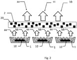
- Fig. 2 shows a schematic of a further embodiment of the light emitting component.
- the light emitting component comprises a light source 10 for emitting blue light, a first layer 1 comprising red phosphor and a second layer 2 comprising luminescent crystals 20.
- the red phosphor of the first layer upon absorption of the blue light aa, emits light in the red light spectrum bb.
- the first layer 1 is arranged adjacent to the light source 10.
- the luminescent crystals 20 of the second layer 2 are of perovskite structure. Upon absorption of the light emitted by the light source 10, the luminescent crystals 20 emit light of a wavelength in the green light spectrum cc.
- the second layer 2 has a haze h 2 of 40% ⁇ h 2 ⁇ 90%.
- the second layer 2 is arranged remotely from the first layer 1. In particular, there is an air gap between the second layer 2 and the first layer 1.
- not only one but multiple light sources 10 and their respective first layers 1 are arranged in an array, wherein the second layer 2 that serves as the second layer 2 for all light sources 10 and their respective first layer 1, is formed in one piece.
- Fig. 3 shows a schematic of a light emitting component for a specific backlight architecture, in particular for LCD displays.
- a diffusor plate 3 arranged between the first layer 1 and the second layer 2.
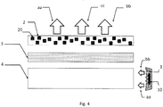
- Fig. 4 shows a further schematic of a further light emitting device for a specific backlight architecture, in particular for LCD displays.
- the device comprises a light emitting component with a light source 10 for emitting blue light aa, a first layer 1 comprising red phosphor, and a second layer 2 comprising luminescent crystals 20.
- the first layer 1 is arranged adjacent to the light source 10.
- the second layer 2 is arranged remotely from the first layer 1.
- a diffusor film 3 and a light guide plate (LGP) 4 are arranged in between the first layer 1 and the second layer 2.
- the light source 10 and the first layer 1 are arranged such that blue aa and the red bb light enter the LGP 4 in an angle of 90° in regard of the light emitted by the LGP 4 that excites the luminescent crystals 20 of the second layer 2.
- the light source 20 might in another advantageous embodiment be arranged such that the light enters the LGP in an angle of 0°.
- Fig. 5 discloses a schematic of an advantageous light emitting device according to an embodiment of the invention.
- the light emitting device in particular an liquid crystal display comprises the light emitting component, e.g. as shown in one of the embodiments in Fig. 1 to 4 .
- An advantageous light emitting device comprises a light emitting component comprising an array of one or more, in particular more than one, light sources 10.
- Each light source 10 comprises its respective first layer 1 arranged adjacent to the light source 10.
- such an embodiment comprises one second layer 2 arranged remotely to the array.
- the array covers essentially the full liquid crystal display area 5.
- a further advantageous light emitting device comprises the one or more of the light sources 10 of the array, wherein each light source 10 is adapted to switch between on and off with a frequency f of f ⁇ 150 Hz, in particular of f ⁇ 300 Hz, very particular of f ⁇ 600 Hz.
- Fig. 2a shows an emission spectrum of an embodiment of a light emitting component according to the invention as shown schematically in Fig. 2b .
- the light emitting component comprises multiple light sources 10 for emitting blue light aa, each light source comprises a respective first layer 1 comprising red phosphor and upon absorption of the blue light aa, the red phosphor emits light in the red light spectrum bb.
- the red phosphors are arranged adjacent to the respective light source 10.
- a second layer 2 comprising luminescent crystals 20 is arranged remotely to the multiple light sources 10 and their respective first layers 2. Upon absorption of the light emitted by the light sources 10, the luminescent crystals 20 emit light of a wavelength in the green light spectrum cc.
- the second layer 2 has a haze of 10% ⁇ h2 ⁇ 100%.
- the emission spectrum of the light emitting device shown in Fig. 2a shows peaks in the range of the blue, green and red visible light.
- Example 1 Preparation of a backlight unit for a LCD display by using a component as described herein
- Fig. 6b shows the schematic of a component of an array for which the emission spectrum was measured an is shown in Fig. 6a .
- the component in Fig. 6b comprises a light source 10 for emitting blue light aa and a first layer 1 comprising red phosphor emitting red light bb.
- the red phosphor particles of the red layer 1 are selected from core-shell CdSe QDs, core-shell InP QDs, KSF phosphor (K 2 SiF 6 :Mn 4+ ). Upon absorption of the blue light aa, the red phosphor emits light in the red light spectrum bb.
- the emission spectrum of the component shows peaks in the visible blue and red range of the spectrum.
- the component shown in Fig. 1b shows the arrangement of the light source 10 and the first layer 1 that is adjacent to the light source 10.
- the first layer 1 comprises red phosphor particles that are distributed adjacent to the light source 10.
- a 2D-array of 200 individual LEDs was used whereby the LEDs comprised a blue emitting gallium nitride chip and red emitting core-shell cadmium selenide quantum dots which were deposited directly on the blue LED chip (on-chip).
- the emission spectrum of this LED array is shown in Fig. 6a .
- Example 2 The array from Example 1 was taken and additionally, a diffuser plate 3 is placed on top of the array of light sources with their respective first layer adjacent to the respective light source.
- the diffusor plate serves to homogeneously distribute the generated light of the LEDs, similar to the light emitting component as shown in Fig. 3 .
- a green remote perovskite QD film (self-supporting film) is placed on top of the diffusor plate (only loose placement; no glueing or similar). Then two crossed prism films (crossed BEFs) and a brightness enhancement film (DBEF) are placed on top of the green perovskite film (not shown in the Figure).
- the emission spectrum of the complete backlight structure is measured with a spectrometer (Konica Minolta CS-2000) showing blue, red and green emission peaks, as shown in Figure 7a .
- Example 3 Preparation of a green remote perovskite QD film as a self-supporting film, with low haze h 2 and low T g : Green perovskite QDs with composition formamidinium lead tribromide (FAPbBr 3 ) are synthesized in toluene as follows: Formamidinium lead tribromide (FAPbBr 3 ) was synthesized by milling PbBr 2 and FABr.
- the final concentration of FAPbBr 3 was 1 wt%.
- the mixture was then dispersed by ball milling using yttrium stabilized zirconia beads with a diameter size of 200 ⁇ m at ambient conditions (if not otherwise defined, the atmospheric conditions for all experiments are: 35°C, 1 atm, in air) for a period of 1 h yielding an ink with green luminescence.
- Film formation 0.1 g of the green ink was mixed with an UV curable monomer/crosslinker mixture (0.7 g FA-513AS, Hitachi Chemical, Japan / 0.3 g Miramer M240, Miwon, Korea) containing 1wt% photoinitiator Diphenyl(2,4,6-trimethylbenzoyl) phosphine oxide (TCI Europe, Netherlands) and 2 wt% polymeric scattering particles (Organopolysiloxane, ShinEtsu, KMP-590) in a speed mixer and the toluene was evaporated by vacuum ( ⁇ 0.01 mbar) at room temperature.
- an UV curable monomer/crosslinker mixture 0.7 g FA-513AS, Hitachi Chemical, Japan / 0.3 g Miramer M240, Miwon, Korea
- 1wt% photoinitiator Diphenyl(2,4,6-trimethylbenzoyl) phosphine oxide TCI Europe, Netherlands
- 2 wt% polymeric scattering particles
- the resulting mixture contained 500 ppm Pb as measured with inductively coupled optical emission spectroscopy (ICP-OES) and was then coated with 50 micron layer thickness on a 100 micron barrier film (supplier: I-components (Korea); Product: TBF-1007), then laminated with a second barrier film of the same type. Afterwards the laminate structure was UV-cured for 60 s (UVAcube100 equipped with a mercury lamp and quartz filter, Hoenle, Germany).
- ICP-OES inductively coupled optical emission spectroscopy
- the haze of the obtained QD film is 50% and the transmittance is 85% (measured with Byk Gardner haze meter).
- the glass transition temperature Tg of the UV-cured resin composition was determined by DSC according to DIN EN ISO 11357-2:2014-07 with a starting temperature of -90°C and an end temperature of 250°C and a heating rate of 20 K/min in nitrogen atmosphere (20 ml/min).
- the purging gas was nitrogen (5.0) at 20 ml/min.
- the DSC system DSC 204 F1 Phoenix (Netzsch) was used.
- the T g was determined on the second heating cycle (the first heating from -90°C to 250°C showed overlaying effects besides the glass transition).
- the UV-cured resin composition was removed from the QD film by delaminating the barrier films.
- the measured Tg of the UV-cured resin composition was 75°C.
- the stability of the QD film was tested for 1'000 hours under blue LED light irradiation by placing the QD film into a light box with high blue intensity (supplier: Hoenle; model: LED CUBE 100 IC) with a blue flux on the QD film of 220 mW/cm2 at a QD film temperature of 50°C.
- the change of optical parameters of the QD film after flux testing for 1'000 hours was measured with the same procedure as for measuring the initial performance (described above).
- the change of optical parameters were as following:
- Comparative example 1 for example 3 Preparation of a green remote perovskite QD film with high haze and low T g .
- the as obtained green perovskite QD film showed an emission wavelength of 525 nm, a FWHM of 22 nm ands a y-value of 0.149 (almost identical to the low-haze QD film in experiment 3).
- the LCF of the QD film is 43%.
- the haze of the QD film was 98% and the transmittance is 81%.
- the measured Tg of the UV-cured resin composition was 77°C. It can be seen that the LCF is lower than in experiment 3. A higher haze leads to a lower LCF and a lower haze leads to a higher LCF. Therefore, a lower haze of the QD film is beneficial to have a higher LCF and in turn a higher display efficiency (at specific comparable white point colour coordinates).
- Comparative example 2 for example 3 Preparation of a green remote perovskite QD film with low haze and high T g .
- the procedure was the same as in the procedure of example 3, except the acrylate monomer mixture (0.7 g FA-513AS, Hitachi Chemical, Japan / 0.3 g Miramer M240, Miwon, Korea) was replaced by the following acrylate monomer mixture:
- the as obtained green perovskite QD film showed an emission wavelength of 526 nm, a FWHM of 22 nm and a y-value of 0.153 (almost identical to the low-haze QD film in experiment 3).
- the LCF of the QD film is 49%.
- the haze of the QD film was 51% and the transmittance is 85%.
- the measured Tg of the UV-cured resin composition was 144°C.
Landscapes
- Chemical & Material Sciences (AREA)
- Engineering & Computer Science (AREA)
- Materials Engineering (AREA)
- Organic Chemistry (AREA)
- Inorganic Chemistry (AREA)
- Led Device Packages (AREA)
Priority Applications (9)
| Application Number | Priority Date | Filing Date | Title |
|---|---|---|---|
| EP20176095.6A EP3913033A1 (de) | 2020-05-22 | 2020-05-22 | Lichtemittierendes bauteil, lichtemittierende vorrichtung und bogenförmiges material |
| CN202180029676.1A CN115427534B (zh) | 2020-05-22 | 2021-05-21 | 发光部件、发光装置和片状材料 |
| JP2022570162A JP2023528245A (ja) | 2020-05-22 | 2021-05-21 | 発光コンポーネント、発光デバイス及びシート状材料 |
| KR1020227034549A KR20230015312A (ko) | 2020-05-22 | 2021-05-21 | 발광 구성요소, 발광 장치 및 시트형 물질 |
| TW110118561A TW202208595A (zh) | 2020-05-22 | 2021-05-21 | 發光組件、發光裝置及片狀材料 |
| EP21727475.2A EP4097191A1 (de) | 2020-05-22 | 2021-05-21 | Lichtemittierendes bauteil, lichtemittierende vorrichtung und bogenförmiges material |
| US17/999,600 US20230223501A1 (en) | 2020-05-22 | 2021-05-21 | Light emitting component, a light emitting device and a sheet-like material |
| PCT/EP2021/063671 WO2021234154A1 (en) | 2020-05-22 | 2021-05-21 | Light emitting component, a light emitting device and a sheet-like material |
| JP2024040202A JP2024096697A (ja) | 2020-05-22 | 2024-03-14 | 発光コンポーネント、発光デバイス及びシート状材料 |
Applications Claiming Priority (1)
| Application Number | Priority Date | Filing Date | Title |
|---|---|---|---|
| EP20176095.6A EP3913033A1 (de) | 2020-05-22 | 2020-05-22 | Lichtemittierendes bauteil, lichtemittierende vorrichtung und bogenförmiges material |
Publications (1)
| Publication Number | Publication Date |
|---|---|
| EP3913033A1 true EP3913033A1 (de) | 2021-11-24 |
Family
ID=70804539
Family Applications (1)
| Application Number | Title | Priority Date | Filing Date |
|---|---|---|---|
| EP20176095.6A Withdrawn EP3913033A1 (de) | 2020-05-22 | 2020-05-22 | Lichtemittierendes bauteil, lichtemittierende vorrichtung und bogenförmiges material |
Country Status (1)
| Country | Link |
|---|---|
| EP (1) | EP3913033A1 (de) |
Citations (5)
| Publication number | Priority date | Publication date | Assignee | Title |
|---|---|---|---|---|
| WO2011053635A1 (en) * | 2009-10-30 | 2011-05-05 | Nanosys, Inc. | Light-emitting diode (led) devices comprising nanocrystals |
| EP3282000A1 (de) * | 2016-08-11 | 2018-02-14 | Avantama AG | Feste polymerzusammensetzung |
| WO2018028869A1 (en) | 2016-08-11 | 2018-02-15 | Avantama Ag | Luminescent crystals and manufacturing thereof |
| EP3296378A1 (de) * | 2015-05-14 | 2018-03-21 | Beijing Institute Of Technology | Lumineszentes perowskit/polymer-verbundstoffmaterial, herstellungsverfahren und anwendung |
| WO2019173025A1 (en) * | 2018-03-08 | 2019-09-12 | General Electric Company | Devices including green-emitting phosphors |
-
2020
- 2020-05-22 EP EP20176095.6A patent/EP3913033A1/de not_active Withdrawn
Patent Citations (5)
| Publication number | Priority date | Publication date | Assignee | Title |
|---|---|---|---|---|
| WO2011053635A1 (en) * | 2009-10-30 | 2011-05-05 | Nanosys, Inc. | Light-emitting diode (led) devices comprising nanocrystals |
| EP3296378A1 (de) * | 2015-05-14 | 2018-03-21 | Beijing Institute Of Technology | Lumineszentes perowskit/polymer-verbundstoffmaterial, herstellungsverfahren und anwendung |
| EP3282000A1 (de) * | 2016-08-11 | 2018-02-14 | Avantama AG | Feste polymerzusammensetzung |
| WO2018028869A1 (en) | 2016-08-11 | 2018-02-15 | Avantama Ag | Luminescent crystals and manufacturing thereof |
| WO2019173025A1 (en) * | 2018-03-08 | 2019-09-12 | General Electric Company | Devices including green-emitting phosphors |
Non-Patent Citations (1)
| Title |
|---|
| HELEEN F. SIJBOM ET AL: "Paper No S6.4: K 2 SiF 6 :Mn 4+ as a Red Phosphor for Remote Phosphor LEDs", S I D INTERNATIONAL SYMPOSIUM. DIGEST OF TECHNICAL PAPERS, vol. 46, no. S1, 1 September 2015 (2015-09-01), US, pages 28 - 28, XP055735676, ISSN: 0097-966X, DOI: 10.1002/sdtp.10565 * |
Similar Documents
| Publication | Publication Date | Title |
|---|---|---|
| EP4069800B1 (de) | Feste polymerzusammensetzung, selbsttragende folie und lichtemittierende vorrichtung | |
| JP2024096697A (ja) | 発光コンポーネント、発光デバイス及びシート状材料 | |
| US11803084B2 (en) | Light emitting component and light emitting device | |
| US12092845B2 (en) | Color conversion film comprising inorganic separation layer | |
| US20220396730A1 (en) | Solid polymer composition, a self-supporting film and a light emitting device | |
| EP3913033A1 (de) | Lichtemittierendes bauteil, lichtemittierende vorrichtung und bogenförmiges material | |
| TW202208595A (zh) | 發光組件、發光裝置及片狀材料 |
Legal Events
| Date | Code | Title | Description |
|---|---|---|---|
| PUAI | Public reference made under article 153(3) epc to a published international application that has entered the european phase |
Free format text: ORIGINAL CODE: 0009012 |
|
| STAA | Information on the status of an ep patent application or granted ep patent |
Free format text: STATUS: THE APPLICATION HAS BEEN PUBLISHED |
|
| AK | Designated contracting states |
Kind code of ref document: A1 Designated state(s): AL AT BE BG CH CY CZ DE DK EE ES FI FR GB GR HR HU IE IS IT LI LT LU LV MC MK MT NL NO PL PT RO RS SE SI SK SM TR |
|
| B565 | Issuance of search results under rule 164(2) epc |
Effective date: 20201012 |
|
| STAA | Information on the status of an ep patent application or granted ep patent |
Free format text: STATUS: THE APPLICATION IS DEEMED TO BE WITHDRAWN |
|
| 18D | Application deemed to be withdrawn |
Effective date: 20220525 |