EP3913687A1 - Elektronisches bauelement mit heteroübergang mit einer feldplatte und einem p-dotierten schwebenden bereich - Google Patents
Elektronisches bauelement mit heteroübergang mit einer feldplatte und einem p-dotierten schwebenden bereich Download PDFInfo
- Publication number
- EP3913687A1 EP3913687A1 EP21174012.1A EP21174012A EP3913687A1 EP 3913687 A1 EP3913687 A1 EP 3913687A1 EP 21174012 A EP21174012 A EP 21174012A EP 3913687 A1 EP3913687 A1 EP 3913687A1
- Authority
- EP
- European Patent Office
- Prior art keywords
- layer
- electrode
- floating region
- barrier layer
- component
- Prior art date
- Legal status (The legal status is an assumption and is not a legal conclusion. Google has not performed a legal analysis and makes no representation as to the accuracy of the status listed.)
- Granted
Links
Images



Classifications
-
- H—ELECTRICITY
- H10—SEMICONDUCTOR DEVICES; ELECTRIC SOLID-STATE DEVICES NOT OTHERWISE PROVIDED FOR
- H10D—INORGANIC ELECTRIC SEMICONDUCTOR DEVICES
- H10D8/00—Diodes
- H10D8/60—Schottky-barrier diodes
-
- H—ELECTRICITY
- H10—SEMICONDUCTOR DEVICES; ELECTRIC SOLID-STATE DEVICES NOT OTHERWISE PROVIDED FOR
- H10D—INORGANIC ELECTRIC SEMICONDUCTOR DEVICES
- H10D30/00—Field-effect transistors [FET]
- H10D30/40—FETs having zero-dimensional [0D], one-dimensional [1D] or two-dimensional [2D] charge carrier gas channels
- H10D30/47—FETs having zero-dimensional [0D], one-dimensional [1D] or two-dimensional [2D] charge carrier gas channels having two-dimensional [2D] charge carrier gas channels, e.g. nanoribbon FETs or high electron mobility transistors [HEMT]
- H10D30/471—High electron mobility transistors [HEMT] or high hole mobility transistors [HHMT]
- H10D30/475—High electron mobility transistors [HEMT] or high hole mobility transistors [HHMT] having wider bandgap layer formed on top of lower bandgap active layer, e.g. undoped barrier HEMTs such as i-AlGaN/GaN HEMTs
-
- H—ELECTRICITY
- H10—SEMICONDUCTOR DEVICES; ELECTRIC SOLID-STATE DEVICES NOT OTHERWISE PROVIDED FOR
- H10D—INORGANIC ELECTRIC SEMICONDUCTOR DEVICES
- H10D62/00—Semiconductor bodies, or regions thereof, of devices having potential barriers
- H10D62/10—Shapes, relative sizes or dispositions of the regions of the semiconductor bodies; Shapes of the semiconductor bodies
- H10D62/102—Constructional design considerations for preventing surface leakage or controlling electric field concentration
- H10D62/103—Constructional design considerations for preventing surface leakage or controlling electric field concentration for increasing or controlling the breakdown voltage of reverse-biased devices
- H10D62/105—Constructional design considerations for preventing surface leakage or controlling electric field concentration for increasing or controlling the breakdown voltage of reverse-biased devices by having particular doping profiles, shapes or arrangements of PN junctions; by having supplementary regions, e.g. junction termination extension [JTE]
- H10D62/106—Constructional design considerations for preventing surface leakage or controlling electric field concentration for increasing or controlling the breakdown voltage of reverse-biased devices by having particular doping profiles, shapes or arrangements of PN junctions; by having supplementary regions, e.g. junction termination extension [JTE] having supplementary regions doped oppositely to or in rectifying contact with regions of the semiconductor bodies, e.g. guard rings with PN or Schottky junctions
-
- H—ELECTRICITY
- H10—SEMICONDUCTOR DEVICES; ELECTRIC SOLID-STATE DEVICES NOT OTHERWISE PROVIDED FOR
- H10D—INORGANIC ELECTRIC SEMICONDUCTOR DEVICES
- H10D62/00—Semiconductor bodies, or regions thereof, of devices having potential barriers
- H10D62/80—Semiconductor bodies, or regions thereof, of devices having potential barriers characterised by the materials
- H10D62/82—Heterojunctions
- H10D62/824—Heterojunctions comprising only Group III-V materials heterojunctions, e.g. GaN/AlGaN heterojunctions
-
- H—ELECTRICITY
- H10—SEMICONDUCTOR DEVICES; ELECTRIC SOLID-STATE DEVICES NOT OTHERWISE PROVIDED FOR
- H10D—INORGANIC ELECTRIC SEMICONDUCTOR DEVICES
- H10D62/00—Semiconductor bodies, or regions thereof, of devices having potential barriers
- H10D62/80—Semiconductor bodies, or regions thereof, of devices having potential barriers characterised by the materials
- H10D62/85—Semiconductor bodies, or regions thereof, of devices having potential barriers characterised by the materials being Group III-V materials, e.g. GaAs
- H10D62/8503—Nitride Group III-V materials, e.g. AlN or GaN
-
- H—ELECTRICITY
- H10—SEMICONDUCTOR DEVICES; ELECTRIC SOLID-STATE DEVICES NOT OTHERWISE PROVIDED FOR
- H10D—INORGANIC ELECTRIC SEMICONDUCTOR DEVICES
- H10D64/00—Electrodes of devices having potential barriers
- H10D64/111—Field plates
-
- H—ELECTRICITY
- H10—SEMICONDUCTOR DEVICES; ELECTRIC SOLID-STATE DEVICES NOT OTHERWISE PROVIDED FOR
- H10D—INORGANIC ELECTRIC SEMICONDUCTOR DEVICES
- H10D64/00—Electrodes of devices having potential barriers
- H10D64/111—Field plates
- H10D64/112—Field plates comprising multiple field plate segments
-
- H—ELECTRICITY
- H10—SEMICONDUCTOR DEVICES; ELECTRIC SOLID-STATE DEVICES NOT OTHERWISE PROVIDED FOR
- H10D—INORGANIC ELECTRIC SEMICONDUCTOR DEVICES
- H10D64/00—Electrodes of devices having potential barriers
- H10D64/20—Electrodes characterised by their shapes, relative sizes or dispositions
- H10D64/27—Electrodes not carrying the current to be rectified, amplified, oscillated or switched, e.g. gates
- H10D64/311—Gate electrodes for field-effect devices
- H10D64/411—Gate electrodes for field-effect devices for FETs
- H10D64/511—Gate electrodes for field-effect devices for FETs for IGFETs
- H10D64/517—Gate electrodes for field-effect devices for FETs for IGFETs characterised by the conducting layers
- H10D64/518—Gate electrodes for field-effect devices for FETs for IGFETs characterised by the conducting layers characterised by their lengths or sectional shapes
-
- H—ELECTRICITY
- H10—SEMICONDUCTOR DEVICES; ELECTRIC SOLID-STATE DEVICES NOT OTHERWISE PROVIDED FOR
- H10D—INORGANIC ELECTRIC SEMICONDUCTOR DEVICES
- H10D64/00—Electrodes of devices having potential barriers
- H10D64/20—Electrodes characterised by their shapes, relative sizes or dispositions
- H10D64/27—Electrodes not carrying the current to be rectified, amplified, oscillated or switched, e.g. gates
- H10D64/311—Gate electrodes for field-effect devices
- H10D64/411—Gate electrodes for field-effect devices for FETs
- H10D64/511—Gate electrodes for field-effect devices for FETs for IGFETs
- H10D64/512—Disposition of the gate electrodes, e.g. buried gates
- H10D64/513—Disposition of the gate electrodes, e.g. buried gates within recesses in the substrate, e.g. trench gates, groove gates or buried gates
Definitions
- the present invention relates to power electronic components based on heterojunction, such as high electron mobility transistors (or HEMTs) and Schottky side diodes based on nitride. galium (GaN).
- heterojunction such as high electron mobility transistors (or HEMTs) and Schottky side diodes based on nitride. galium (GaN).
- a heterojunction is formed by the junction of two semiconductor materials with different bandgap widths.
- a heterojunction of the AlGaN / GaN type comprises a layer of galium nitride (GaN) surmounted by a layer of aluminum-gallium nitride (AlGaN).
- GaN galium nitride
- AlGaN aluminum-gallium nitride
- a two-dimensional electron gas (or 2DEG, for "2-Dimensional Electron Gas” in English) forms at the interface between the AlGaN layer and the GaN layer, due to spontaneous polarization and piezoelectric polarization.
- This two-dimensional electron gas serves as a conduction channel within heterojunction electronic components, such as HEMT transistors and Schottky side diodes.
- Heterojunction electronic components withstand high current densities in the on state, due to the high density of charge carriers (electrons) and the high mobility of these carriers in two-dimensional electron gas. For certain applications such as high voltage switching, it is important that these electronic components also exhibit good voltage withstand in the off state, in other words a high breakdown voltage.
- this transistor comprises a substrate 10, a buffer layer 11 of p-doped GaN (p-GaN) disposed on the substrate 10, a channel layer 12 of n-doped GaN (n-GaN) disposed on the buffer layer 11, a layer barrier 13 in n-doped AlGaN (n-AlGaN) arranged on the channel layer 12 and a passivation layer 14 arranged on the barrier layer 13.
- the channel layer 12 in n-GaN and the barrier layer 13 in n-AlGaN form a heterojunction 20.
- a two-dimensional electron gas 21 is inherently formed at the interface between the channel layer 12 and the barrier layer 13. This two-dimensional electron gas 21 is shown in dotted lines on the diagram. figure 1 .
- the transistor further comprises a gate electrode 15, extending through the passivation layer 14 to contact the barrier layer 13, drain and source electrodes 16-17 interconnected by the electron gas.
- a gate electrode 15 extending through the passivation layer 14 to contact the barrier layer 13, drain and source electrodes 16-17 interconnected by the electron gas.
- two-dimensional 21 and two field plates 18a-18b arranged on the passivation layer 14, respectively forming extensions of the gate electrode 15 and of the drain electrode 16.
- the p-GaN buffer layer 11 and the n-GaN channel layer 12 together form a PN junction under the heterojunction, which improves the confinement of the two-dimensional electron gas by creating a buried potential barrier ("back-barrier " in English).
- the PN junction and the field plates 18a-18b redistribute the electric field more uniformly in the component, which has the consequence of increasing the breakdown voltage of the transistor (i.e. the maximum allowable voltage between the drain and the source in the blocked state).
- the PN junction also has the effect of partially depleting the two-dimensional electron gas 21, resulting in an increase in the on-resistance of the component, by about 14% compared to a structure without a PN junction. .
- the document US2015 / 270355 describes another AlGaN / GaN heterojunction transistor, comprising a GaN channel layer, an AlGaN barrier layer disposed on the channel layer, a source electrode, a drain electrode, a gate electrode and a field plate forming an extension of the source electrode.
- the transistor further comprises a floating layer of p-doped AlGaN arranged on the barrier layer between the gate electrode and the drain electrode, in line with a flank of the field plate.
- This p-doped AlGaN floating layer called RESURF (for “Reduced Surface Field”), reduces the electric field in the passivation layer separating the field plate and the gate electrode, in particular the field peaks at the end of the field plate and at the end of the gate electrode. This effect of reducing the electric field remains however limited to the passivation layer.
- the object of the invention is to increase the breakdown voltage of a heterojunction electronic component while limiting the increase in its electrical resistance in the on state.
- the p-doped floating region located in the barrier layer reduces the electric field in the passivation layer but also in the barrier layer, which results in an increase in the breakdown voltage of the component. Furthermore, this floating region confines the two-dimensional electron gas of the heterojunction to a lesser extent than a confining layer disposed below the channel layer. The increase in the breakdown voltage is therefore not done to the detriment of a significant degradation of the other electrical characteristics of the component, in particular of its on-state resistance.
- the floating region is disposed on the barrier layer, and not within the boundaries of the barrier layer.
- the electric (lateral) field in the barrier layer is not diminished but transferred and concentrated at the distal end of the floating region. This results in a risk of component breakdown at this transfer point.
- the electric field is also increased in the two-dimensional electron gas (forming part of the conduction channel of the transistor), which can lead to the appearance of hot carriers when switching the transistor.
- the component further comprises a first electrode and a second electrode separated from the first electrode by at least part of the passivation layer.
- the component is of the diode type
- the first electrode is an anode
- the second electrode is a cathode
- the component is of the transistor type
- the first electrode is a gate electrode
- the second electrode is a drain electrode
- the component comprises a plurality of field plates and a plurality of floating regions of p-type doped semiconductor material, each floating region being located in the barrier layer directly above it. 'a flank of one of the field plates.
- the figure 2 shows a schematic sectional view of a first embodiment of a heterojunction electronic component 1.
- This type of component finds advantageous applications in power electronics, for example as a power switch.
- Component 1 can thus switch reversibly between a first state called “on state” (or “ON state”) and a second state called “blocked state” (or “OFF state”).
- Component 1 comprises a substrate 10 and a heterojunction 20 disposed on the substrate 10.
- the heterojunction 20 comprises a first semiconductor layer 12, commonly referred to as a "channel layer” and disposed on the substrate 10, and a second semiconductor layer.
- conductive 13 commonly called a “barrier layer” and disposed on the channel layer 12.
- a two-dimensional electron gas 21 (or 2DEG, for “2-Dimensional Electron Gas” in English) is formed intrinsically (by heterojunction) at the interface between the channel layer 12 and the barrier layer 13. On the figure 2 , it is symbolized by dotted lines in the channel layer 16 along the interface between the channel layer 16 and the barrier layer 17.
- the substrate 10 is for example made of silicon (Si), of silicon carbide (SiC), of galium nitride (GaN) or of sapphire (Al 2 O 3 ).
- Channel layer 12 and barrier layer 13 are formed from semiconductor materials having different bandgap widths.
- the channel layer 12 and the barrier layer 13 are preferably layers of III-V semiconductor material, for example based on GaN (made of GaN or GaN alloy such as AlGaN, InGaN, etc.).
- the heterojunction 20 is for example of the GaN / AlGaN type.
- Channel layer 12 then consists of galium nitride, preferably unintentionally doped (UID GaN), while barrier layer 13 consists of aluminum-galium nitride, preferably unintentionally doped (UID AlGaN).
- a semiconductor material is considered to be unintentionally doped when its concentrations of donor-type and acceptor-type dopants are less than 10 16 cm -3 (NA ⁇ 10 16 cm -3 and ND ⁇ 10 16 cm -3 ).
- the layer channel 12 has a thickness of between 20 nm and 500 nm
- barrier layer 13 has a thickness of between 2 nm and 30 nm. The thickness of a layer is measured in a direction perpendicular to the substrate 10.
- the channel layer 12 and the barrier layer 13 can be respectively in GaAs and Al x Ga 1-x As (x ⁇ 0.25), or in Ga y ln 1-y As (y ⁇ 0.8) and AlxGai-xAs (x ⁇ 0.25).
- the heterojunction 20 can also include an intermediate layer (not shown in the figure), interposed between the channel layer 12 and the barrier layer 13, to increase the density and mobility of electrons in the two-dimensional electron gas 21.
- a such an intermediate layer is typically extremely thin (for example 1 nm thick) and may consist of aluminum nitride (AlN), this material being particularly suitable for the interface between a channel layer 12 made of GaN and a layer barrier 13 in AlGaN.
- component 1 advantageously comprises a semi-insulating buffer layer 11 disposed between substrate 10 and channel layer 12.
- This buffer layer 11 limits lateral and vertical leakage currents in component 1 and improves its voltage withstand ( lateral) in the blocked state, in other words its ability to withstand high reverse voltages.
- the buffer layer 11 preferably comprises a semiconductor material, such as GaN or AlGaN. This semiconductor material can be doped with impurities, such as carbon atoms.
- the buffer layer 11 can in particular be formed by a single GaN: C layer or by a GaN: C / Al x Ga 1-x N bilayer, with x ranging between 4% and 8% approximately.
- the thickness of the buffer layer 11 is chosen as a function of the breakdown voltage desired for the component 1. It is for example between 1 ⁇ m and 15 ⁇ m.
- component 1 may further comprise a transition layer (not shown in the figures) arranged between substrate 10 and the layer. channel layer 12, and more particularly between the substrate 10 and the buffer layer 11.
- This transition layer makes it possible to adapt the crystal lattice parameter and to manage the mechanical stresses between the substrate 10 and the layers of the heterojunction 20.
- It may include a nucleation sublayer (for example an AlN layer of 100 nm thick), in contact with the substrate 10, and several adaptation sublayers stacked on the nucleation sublayer.
- the adaptation sublayers include, for example, AlGaN, the aluminum content of which varies from one layer to another (for example several layers of AlGaN with a molar fraction of AlN which decreases with the distance relative to the substrate 10, or a superlattice comprising several bilayers Al x Ga 1-x N / GaN).
- Component 1 also comprises a passivation layer 14 disposed on the barrier layer 13, a first electrode 15 and a second electrode 16 separated (laterally) from the first electrode 15 by at least part of the passivation layer 14.
- the first electrode 15 and the second electrode 16 rest for example on a lower portion of the channel layer 12.
- An upper portion of the channel layer 12, the barrier layer 13 and at least a portion of the passivation layer 14 extend between the first electrode 15 and the second electrode 16.
- the passivation layer 14 may consist of a single electrically insulating material, for example silicon dioxide (SiO 2 ), silicon nitride (Si 3 N 4 ), aluminum nitride (AlN) or alumina (Al 2 O 3 ).
- the passivation layer may include several stacked sublayers formed from different insulating materials, typically an alternation of oxide (eg SiO 2 ) and nitride (eg SiN) sublayer. These different sublayers serve as a support for the production of one or more field plates, described below.
- Each of the first and second electrodes 15-16 can be made of a metallic material, preferably chosen from aluminum (Al), copper (Cu), gold (Au), titanium (Ti), nitride titanium (TiN) and nickel (Ni), or several stacked metallic materials.
- the material (s) used to form the first electrode 15 may be different from the material (s) used to form the second electrode 16.
- the first electrode 15 is made of nickel (barrier metal compound, annealed at low temperature) and second electrode 16 is made of an Al / Ti stack.
- component 1 is a Schottky side diode.
- the first electrode 15 is an anode, in Schottky contact with the two-dimensional electron gas 21, and the second electrode 16 is a cathode, in contact ohmic with the two-dimensional electron gas 21.
- the anode and cathode are located at opposite ends of the two-dimensional electron gas 21. They are connected by the two-dimensional electron gas 21.
- Component 1 further comprises a first field plate 18a, associated with the first electrode 15 and separated from the barrier layer 13 by a first portion 14a (typically a sub-layer) of the passivation layer 14.
- the first field plate 18a may form an extension of the first electrode 15, which preferably extends parallel to the barrier layer 13 towards the second electrode 16. In other words, it may be formed by a protruding portion of the first electrode. 15.
- the first field plate 18a may be formed from the same metallic material (s) as the first electrode 15 or from one (or more) different metallic material (s). (s).
- the first portion 14a of the passivation layer 14 preferably has a constant thickness.
- component 1 comprises a second field plate 18b, associated with second electrode 16 and separated from barrier layer 13 by a second portion 14b of passivation layer 14 (preferably of constant thickness).
- the second field plate 18b may form an extension of the second electrode 16, which preferably extends parallel to the barrier layer 13 towards the first electrode 15.
- the field plates 18a-18b reduce the electric field peaks due to the abrupt discontinuities between the different materials of component 1. They distribute the electric field more uniformly within component 1 and improve its voltage withstand.
- component 1 comprises a floating region 19 located in barrier layer 13 directly above a side of first field plate 18a.
- a floating region refers to a region subject to no external electrical polarization (i.e. no electrical potential is applied to that region), unlike the first and second electrodes 15-16.
- the floating region 19 is electrically isolated from the electrodes of component 1.
- a first portion of the barrier layer 13 separates the floating region 19 from the first electrode 15 and a second portion of the barrier layer 13 separates the floating region 19 from the second. electrode 16.
- the flank of the first field plate 18a, under which the floating region 19 is located, is that furthest from the first electrode 15. In other words, the floating region 19 is located directly above a distal end. of the first field plate 18a (relative to the first electrode 15).
- the floating region 19 is made of a p-type doped semiconductor material. This semiconductor material is advantageously the same as that forming the barrier layer 13, in this example AlGaN. Thus, the manufacture of component 1 is simplified.
- the floating region 19 can in particular be formed by doping with p-type doping impurities (for example magnesium ions) a portion of the barrier layer 13.
- the floating region 19 has a thickness less than that of the barrier layer 13, so as not to interrupt the two-dimensional electron gas 21 between the first electrode 15 and the second electrode 16.
- the floating region 19 is advantageously in direct contact with the gas. passivation layer 14, as shown in figure 2 .
- the floating region 19 can thus be produced more easily and at a lower cost.
- the floating region 19 has in a plane parallel to the substrate 10 at least one dimension smaller than that of the barrier layer 13. In other words, the floating region 19 occupies only a part of the barrier layer 13 in a plane parallel to the substrate. 10. More precisely, in the section plane of the figure 2 , the floating region 19 has a width L FZ less than the width L BL of the barrier layer 13, ie the distance between the first and second electrodes 15-16.
- the floating region 19 reduces (at a given reverse voltage) the electric field in the portion of the passivation layer 14 located above the floating region 19 and in the portion of the barrier layer 13 separating the floating region 19 from the layer. channel 12, and more particularly vertically to the side of the first field plate 18a. These two areas of the component are usually limiting in terms of voltage withstand, because the electric field is very strong there.
- the reduction of the electric field in the passivation layer 14 and in the barrier layer 13 is the result of a greater ionization of the doping impurities of the donor type (thanks to the free charge carriers - holes - provided by the floating region 19) at the interface between the passivation layer 14 and the layer barrier 13.
- the increase in the density of ionized donors at the interface locally lowers the conduction band in the floating region 19 and in the passivation layer 14, which compensates for the increase in the conduction band due to the presence of. the doped region p.
- the latter can withstand a higher reverse voltage.
- the component breakdown voltage is therefore increased.
- the figure 3 represents the direct current density I F of a side Schottky diode according to the figure 2 as a function of the forward bias voltage V F and, for comparison, the forward current density I F of a Schottky side diode devoid of a floating region 19 in the barrier layer 13.
- the figure 4 represents the reverse current density I R as a function of the reverse bias voltage V R for these same two Schottky side diodes. Again, the curves overlap. The floating region 19 therefore has no influence on the reverse leakage current of the diode. Note that the figure 4 does not represent the breakdown voltage of the diode.
- the floating region 19 disposed in the barrier layer 13 has a limited negative impact on the performance of component 1, and in particular its on-state resistance.
- the floating region 19 is advantageously centered (i.e. arranged symmetrically) with respect to the flank of the first field plate 18a, in order to minimize the electric field in the barrier layer 13 and the passivation layer. 14. It can also be slightly offset, towards the first electrode 15 or the second electrode 16, as long as it is crossed by the vertical projection of the side of the first field plate 18a.
- the width L FZ of the floating region 19 (measured parallel to the substrate 10 in the section plane of the figure 2 ) is preferably less than twice the width L FP of the first field plate 18a. Thus, when the floating region 19 is centered relative to the (outer) flank of the first field plate 18a, it does not come into contact with the first electrode 15.
- the concentration of p-type doping impurities (activated) in the floating region 19 is advantageously between 1.10 18 cm -3 and 2.10 19 cm -3 , in order to obtain a significant reduction in the electric field without excessively reducing the density. electrons in the two-dimensional electron gas 21.
- the thickness of the floating region 19 may be between 10% and 90% of the thickness of the barrier layer 13.
- component 1 comprises several field plates 18a associated with first electrode 15 and several p-doped floating regions 19, as described above.
- the field plates 18a preferably form extensions of the first electrode 15 (or protrusions of the first electrode 15 into the passivation layer 14). They can be separated two by two by a portion (typically an underlayer) of the passivation layer 14 or, as shown in Figure figure 5 , in contact with each other, for example in the form of staircase steps.
- Each of the floating regions 19 is located in the barrier layer 13 vertically to at least one side of the field plate (some of which form a transition between two successive field plates), and preferably vertical to one side of the field plate. 'a single field plate.
- Each floating region 19 reduces the electric field locally, that is to say in the portions of the passivation layer 14 and of the barrier layer 13 placed opposite each other.
- a field plate 19 disposed under one side of a (single) field plate 18a has no effect on the electric field under the side of the adjacent field plate 18a.
- each field plate 18a is associated with a single floating region 19.
- component 1 may comprise N field plates 18a associated with the first electrode 15 and M floating regions 19, N and M being natural numbers greater than or equal to 2 and M being less than or equal to N.
- component 1 is a heterojunction transistor, also called a high electron mobility transistor (or HEMT, for “High Electron Mobility Transistor”).
- the first electrode is a gate electrode, isolated from the heterojunction 20 by a dielectric layer 22, typically made of an oxide called "gate oxide”, and the second electrode 16 is a drain electrode.
- the transistor comprises a third electrode 17 forming a source electrode.
- the gate electrode 15 of the transistor is disposed between the drain and source electrodes 16-17. It can split the two-dimensional electron gas 21 into two by extending through the barrier layer 13 and part of the channel layer 12, as shown in the figure. figure 6 , or on the contrary leave it whole and stop on the barrier layer 13.
- the drain electrode 16 and the source electrode 17 are located at opposite ends of the two-dimensional electron gas 21. When the transistor is in the on state, they are electrically connected by the two-dimensional electron gas 21 and a conduction channel, formed by an inversion layer which accumulates electrons along the gate oxide layer.
- the heterojunction transistor may include a single gate-side field plate 18a and a single floating region 19, as described in connection with figure 2 , or several (N) field plates 18a on the gate side and several (M ⁇ N) floating regions 19, as described in connection with figure 5 .
- the field plates 18a and the floating regions 19 are located between the gate electrode 15 and the drain electrode 16 (where the electric field is strongest).
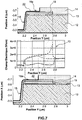
- the figure 7 represents the electric field in absolute value in the barrier layer 13 of a heterojunction transistor according to an exemplary embodiment of the invention (in solid line) and, by way of comparison, that of a transistor according to the document US2015 / 270355 (in dotted line) and that of a transistor without a floating region (in phantom).
- the transistor according to the invention (shown at the bottom of the figure) here comprises a field plate 18a extending from the gate 15 and a single floating region 19.
- the electric field is simulated at 1 nm below the interface between the barrier layer. 13 and the passivation layer 14 (or between the barrier layer 13 and the floating region 19 in the case of document US2015 / 270355 ).
- the figure 7 shows that when the floating region 19 is introduced into the barrier layer 13, the electric field is reduced in the barrier layer 13, in particular under the flank of the field plate 18a (solid line curve vs. phantom line curve) .
- the electric field is on the contrary unchanged under the side of the field plate 18a. Worse, it increases sharply at the distal end of the floating region 19, forming a field peak 70 (dotted line curve).
- the figure 8 represents for these same transistors the electric field in absolute value at 1 nm below the heterojunction, in other words in the region called "channel" where the two-dimensional electron gas is formed (however, in the blocked state, the two-dimensional electron gas is depleted).
- This figure shows that another field peak 80 appears in the channel region, directly above the distal end of the floating region 19, when the latter is located on the barrier layer 13.
- a high field in the region. channel can create hot carriers when switching the transistor and cause its destruction.
- the first and second electrodes 15-16 and the first and second field plates 18a-18b are preferably formed simultaneously.
- the floating region 19 can in particular be formed by implantation of p-type doping impurities (such as magnesium ions) in a portion of the barrier layer 13, preferably through a thin passivation layer (thickness between 3 nm and 20 nm. nm to prevent the channeling of the implanted ions) arranged on the barrier layer 13 and the opening of a mask placed on this passivation layer.
- p-type doping impurities such as magnesium ions
- the barrier layer 13 and the floating region 19 can also be formed by successively growing on the channel layer 12 a first sub-layer of unintentionally doped semiconductor material (eg UID AlGaN) and a second sub-layer of material.
- p-doped semiconductor eg AlGaN
- implanting in regions of the second sublayer arranged on either side of the floating region 19 to be formed
- n-type doping impurities to compensate for the p-doping or hydrogen ions to neutralize p-type doping impurities.
- the same regions of the second sub-layer of p-doped semiconductor material can be etched through openings of a mask, after etching of the thin passivation layer, to delimit the floating region 19, then the barrier layer. 13 is finalized (i.e. completed) by epitaxially growing unintentionally doped semiconductor material outside of the floating region 19.
- the thin passivation layer prevents growth of unintentionally doped semiconductor material above the floating region 19.
- a final technique for forming the floating region 19 comprises the etching of a portion of the barrier layer 13 through the opening of a mask, after etching of the thin passivation layer, then the growth by epitaxy of the material. p-doped semiconductor in the etched area.
- the thin passivation layer prevents the growth of the p-doped semiconductor material outside the etched area.
Landscapes
- Electrodes Of Semiconductors (AREA)
- Junction Field-Effect Transistors (AREA)
- Photovoltaic Devices (AREA)
Applications Claiming Priority (1)
| Application Number | Priority Date | Filing Date | Title |
|---|---|---|---|
| FR2005011A FR3110770B1 (fr) | 2020-05-19 | 2020-05-19 | Composant électronique à hétérojonction comprenant une plaque de champ et une région flottante dopée p |
Publications (2)
| Publication Number | Publication Date |
|---|---|
| EP3913687A1 true EP3913687A1 (de) | 2021-11-24 |
| EP3913687B1 EP3913687B1 (de) | 2025-12-17 |
Family
ID=72178717
Family Applications (1)
| Application Number | Title | Priority Date | Filing Date |
|---|---|---|---|
| EP21174012.1A Active EP3913687B1 (de) | 2020-05-19 | 2021-05-17 | Elektronisches bauelement mit heteroübergang mit einer feldplatte und einem p-dotierten schwebenden bereich |
Country Status (3)
| Country | Link |
|---|---|
| US (1) | US12009416B2 (de) |
| EP (1) | EP3913687B1 (de) |
| FR (1) | FR3110770B1 (de) |
Cited By (1)
| Publication number | Priority date | Publication date | Assignee | Title |
|---|---|---|---|---|
| CN114678415A (zh) * | 2022-03-28 | 2022-06-28 | 江苏晶曌半导体有限公司 | 一种具有阵列浮空岛结构的氮化镓肖特基二极管器件 |
Families Citing this family (3)
| Publication number | Priority date | Publication date | Assignee | Title |
|---|---|---|---|---|
| EP3975246A1 (de) * | 2020-09-25 | 2022-03-30 | Infineon Technologies Austria AG | Halbleiterchip und verfahren zur herstellung davon |
| CN114582970A (zh) | 2020-12-01 | 2022-06-03 | 联华电子股份有限公司 | 半导体装置及其制作方法 |
| CN118073427A (zh) * | 2024-02-19 | 2024-05-24 | 松山湖材料实验室 | 半导体器件及其制备方法 |
Citations (3)
| Publication number | Priority date | Publication date | Assignee | Title |
|---|---|---|---|---|
| JP2012028409A (ja) * | 2010-07-20 | 2012-02-09 | Advanced Power Device Research Association | 半導体装置 |
| US20150270379A1 (en) * | 2014-03-19 | 2015-09-24 | Kabushiki Kaisha Toshiba | Semiconductor device |
| US20150270355A1 (en) | 2014-03-19 | 2015-09-24 | Kabushiki Kaisha Toshiba | Semiconductor device and manufacturing method for the same |
Family Cites Families (3)
| Publication number | Priority date | Publication date | Assignee | Title |
|---|---|---|---|---|
| JP5481103B2 (ja) * | 2009-06-11 | 2014-04-23 | 株式会社東芝 | 窒化物半導体素子 |
| JP5908692B2 (ja) * | 2011-09-29 | 2016-04-26 | トランスフォーム・ジャパン株式会社 | 化合物半導体装置及びその製造方法 |
| US11398546B2 (en) * | 2019-08-06 | 2022-07-26 | Vanguard International Semiconductor Corporation | Semiconductor devices and methods for fabricating the same |
-
2020
- 2020-05-19 FR FR2005011A patent/FR3110770B1/fr active Active
-
2021
- 2021-05-17 EP EP21174012.1A patent/EP3913687B1/de active Active
- 2021-05-19 US US17/324,612 patent/US12009416B2/en active Active
Patent Citations (3)
| Publication number | Priority date | Publication date | Assignee | Title |
|---|---|---|---|---|
| JP2012028409A (ja) * | 2010-07-20 | 2012-02-09 | Advanced Power Device Research Association | 半導体装置 |
| US20150270379A1 (en) * | 2014-03-19 | 2015-09-24 | Kabushiki Kaisha Toshiba | Semiconductor device |
| US20150270355A1 (en) | 2014-03-19 | 2015-09-24 | Kabushiki Kaisha Toshiba | Semiconductor device and manufacturing method for the same |
Non-Patent Citations (2)
| Title |
|---|
| "RESURF AIGaN/GaN HEMT for high voltage power switching", IEEE ELECTRON DEVICE LETTERS, vol. 22, no. 8, 2001, pages 373 - 375 |
| SEUNG-CHUL LEE ET AL: "High Breakdown Voltage GaN Schottky Barrier Diode employing Floating Metal Rings on AlGaN/GaN Hetero-junction", POWER SEMICONDUCTOR DEVICES AND ICS, 2005. PROCEEDINGS. ISPSD '05. THE 17TH INTERNATIONAL SYMPOSIUM ON SANTA BARBARA, CA, USA MAY 23-26, 2005, PISCATAWAY, NJ, USA,IEEE, 23 May 2005 (2005-05-23), pages 247 - 250, XP010820737, ISBN: 978-0-7803-8890-1, DOI: 10.1109/ISPSD.2005.1487997 * |
Cited By (2)
| Publication number | Priority date | Publication date | Assignee | Title |
|---|---|---|---|---|
| CN114678415A (zh) * | 2022-03-28 | 2022-06-28 | 江苏晶曌半导体有限公司 | 一种具有阵列浮空岛结构的氮化镓肖特基二极管器件 |
| CN114678415B (zh) * | 2022-03-28 | 2022-12-02 | 江苏晶曌半导体有限公司 | 一种具有阵列浮空岛结构的氮化镓肖特基二极管器件 |
Also Published As
| Publication number | Publication date |
|---|---|
| EP3913687B1 (de) | 2025-12-17 |
| US12009416B2 (en) | 2024-06-11 |
| FR3110770B1 (fr) | 2022-04-29 |
| FR3110770A1 (fr) | 2021-11-26 |
| US20210367069A1 (en) | 2021-11-25 |
Similar Documents
| Publication | Publication Date | Title |
|---|---|---|
| EP3913687B1 (de) | Elektronisches bauelement mit heteroübergang mit einer feldplatte und einem p-dotierten schwebenden bereich | |
| TWI450383B (zh) | 半導體結構、包括半導體結構之積體電路及用以製造半導體結構之方法 | |
| CN102308390B (zh) | 半导体异质结构二极管 | |
| US8895423B2 (en) | Method for making semiconductor diodes with low reverse bias currents | |
| EP3203526B1 (de) | Transistor mit heteroübergang mit verbessertem elektronengas-einschluss | |
| EP2421045A1 (de) | Zweite schottky-kontakt-metallschicht zur erhöhung der leistung einer gan-schottky-diode | |
| EP3240041A1 (de) | Selbstsperrender transistor mit heteroübergang und hoher schwellenspannung | |
| EP2736079B1 (de) | Herstellungsverfahren eines Transistors mit Heteroübergang vom Typ, der normalerweise blockiert ist | |
| FR3074359A1 (fr) | Composant electronique a heterojonction muni d'une couche barriere enterree amelioree | |
| FR2969386A1 (fr) | Transistor a haute mobilite electronique dote d'une couche de nitrure de gallium et d'indium | |
| EP4318597A1 (de) | Feldeffekttransistor mit p-fet-verhalten | |
| EP3378098B1 (de) | Heteroübergangdiode mit erhöhtem transientem spitzenstrom | |
| EP3896745B1 (de) | Übergangsbarriere-schottky-diode | |
| EP3561880A1 (de) | Hemt und herstellungsverfahren welches eine geringere gatelänge und einen geringeren gate-leckverlust begünstigt | |
| FR2496990A1 (fr) | Transistor a effet de champ a barriere schottky | |
| CN119008660A (zh) | 一种半导体器件及其制备方法 | |
| EP3792982B1 (de) | Elektronische leistungsvorrichtung mit superjunction | |
| WO2019224448A1 (fr) | Transistor a haute mobilite electronique en mode enrichissement | |
| EP4084085A1 (de) | Mikroelektronische vorrichtung | |
| WO2020035644A1 (fr) | Transistor a haute mobilite electronique | |
| FR3047609A1 (fr) | Transistor hemt de type normalement ouvert presentant une tension de seuil eleve et une resistance de conduction reduite | |
| EP3945605B1 (de) | Halbleiterdiode und herstellungsverfahren einer solchen diode | |
| EP3591709A1 (de) | Selbstsperrender transistor mit heteroübergang und vermindertem durchgangswiderstand | |
| JP2025179877A (ja) | ショットキーバリアダイオード | |
| EP4068386A1 (de) | Transistor mit feldeffekt und vertikaler struktur |
Legal Events
| Date | Code | Title | Description |
|---|---|---|---|
| PUAI | Public reference made under article 153(3) epc to a published international application that has entered the european phase |
Free format text: ORIGINAL CODE: 0009012 |
|
| STAA | Information on the status of an ep patent application or granted ep patent |
Free format text: STATUS: REQUEST FOR EXAMINATION WAS MADE |
|
| 17P | Request for examination filed |
Effective date: 20210517 |
|
| AK | Designated contracting states |
Kind code of ref document: A1 Designated state(s): AL AT BE BG CH CY CZ DE DK EE ES FI FR GB GR HR HU IE IS IT LI LT LU LV MC MK MT NL NO PL PT RO RS SE SI SK SM TR |
|
| B565 | Issuance of search results under rule 164(2) epc |
Effective date: 20211012 |
|
| RBV | Designated contracting states (corrected) |
Designated state(s): AL AT BE BG CH CY CZ DE DK EE ES FI FR GB GR HR HU IE IS IT LI LT LU LV MC MK MT NL NO PL PT RO RS SE SI SK SM TR |
|
| RAP3 | Party data changed (applicant data changed or rights of an application transferred) |
Owner name: COMMISSARIAT A L'ENERGIE ATOMIQUE ET AUX ENERGIESALTERNATIVES |
|
| REG | Reference to a national code |
Ref country code: DE Ref legal event code: R079 Free format text: PREVIOUS MAIN CLASS: H01L0029872000 Ipc: H10D0008600000 Ref document number: 602021044440 Country of ref document: DE |
|
| GRAJ | Information related to disapproval of communication of intention to grant by the applicant or resumption of examination proceedings by the epo deleted |
Free format text: ORIGINAL CODE: EPIDOSDIGR1 |
|
| GRAP | Despatch of communication of intention to grant a patent |
Free format text: ORIGINAL CODE: EPIDOSNIGR1 |
|
| GRAP | Despatch of communication of intention to grant a patent |
Free format text: ORIGINAL CODE: EPIDOSNIGR1 |
|
| STAA | Information on the status of an ep patent application or granted ep patent |
Free format text: STATUS: GRANT OF PATENT IS INTENDED |
|
| RIC1 | Information provided on ipc code assigned before grant |
Ipc: H10D 8/60 20250101AFI20250618BHEP Ipc: H10D 30/47 20250101ALI20250618BHEP Ipc: H10D 62/10 20250101ALI20250618BHEP Ipc: H10D 62/824 20250101ALI20250618BHEP Ipc: H10D 64/00 20250101ALI20250618BHEP Ipc: H10D 64/27 20250101ALI20250618BHEP Ipc: H10D 62/85 20250101ALN20250618BHEP |
|
| RIC1 | Information provided on ipc code assigned before grant |
Ipc: H10D 8/60 20250101AFI20250624BHEP Ipc: H10D 30/47 20250101ALI20250624BHEP Ipc: H10D 62/10 20250101ALI20250624BHEP Ipc: H10D 62/824 20250101ALI20250624BHEP Ipc: H10D 64/00 20250101ALI20250624BHEP Ipc: H10D 64/27 20250101ALI20250624BHEP Ipc: H10D 62/85 20250101ALN20250624BHEP |
|
| INTG | Intention to grant announced |
Effective date: 20250709 |
|
| GRAS | Grant fee paid |
Free format text: ORIGINAL CODE: EPIDOSNIGR3 |
|
| GRAA | (expected) grant |
Free format text: ORIGINAL CODE: 0009210 |
|
| STAA | Information on the status of an ep patent application or granted ep patent |
Free format text: STATUS: THE PATENT HAS BEEN GRANTED |
|
| AK | Designated contracting states |
Kind code of ref document: B1 Designated state(s): AL AT BE BG CH CY CZ DE DK EE ES FI FR GB GR HR HU IE IS IT LI LT LU LV MC MK MT NL NO PL PT RO RS SE SI SK SM TR |
|
| REG | Reference to a national code |
Ref country code: CH Ref legal event code: F10 Free format text: ST27 STATUS EVENT CODE: U-0-0-F10-F00 (AS PROVIDED BY THE NATIONAL OFFICE) Effective date: 20251217 Ref country code: GB Ref legal event code: FG4D Free format text: NOT ENGLISH |
|
| REG | Reference to a national code |
Ref country code: DE Ref legal event code: R096 Ref document number: 602021044440 Country of ref document: DE |
|
| REG | Reference to a national code |
Ref country code: LT Ref legal event code: MG9D |
|
| PG25 | Lapsed in a contracting state [announced via postgrant information from national office to epo] |
Ref country code: NO Free format text: LAPSE BECAUSE OF FAILURE TO SUBMIT A TRANSLATION OF THE DESCRIPTION OR TO PAY THE FEE WITHIN THE PRESCRIBED TIME-LIMIT Effective date: 20260317 |
|
| PG25 | Lapsed in a contracting state [announced via postgrant information from national office to epo] |
Ref country code: HR Free format text: LAPSE BECAUSE OF FAILURE TO SUBMIT A TRANSLATION OF THE DESCRIPTION OR TO PAY THE FEE WITHIN THE PRESCRIBED TIME-LIMIT Effective date: 20251217 Ref country code: FI Free format text: LAPSE BECAUSE OF FAILURE TO SUBMIT A TRANSLATION OF THE DESCRIPTION OR TO PAY THE FEE WITHIN THE PRESCRIBED TIME-LIMIT Effective date: 20251217 |
|
| PG25 | Lapsed in a contracting state [announced via postgrant information from national office to epo] |
Ref country code: RS Free format text: LAPSE BECAUSE OF FAILURE TO SUBMIT A TRANSLATION OF THE DESCRIPTION OR TO PAY THE FEE WITHIN THE PRESCRIBED TIME-LIMIT Effective date: 20260317 |
|
| REG | Reference to a national code |
Ref country code: NL Ref legal event code: MP Effective date: 20251217 |
|
| PG25 | Lapsed in a contracting state [announced via postgrant information from national office to epo] |
Ref country code: LV Free format text: LAPSE BECAUSE OF FAILURE TO SUBMIT A TRANSLATION OF THE DESCRIPTION OR TO PAY THE FEE WITHIN THE PRESCRIBED TIME-LIMIT Effective date: 20251217 |