EP3916914B1 - Carte de circuit d'étalonnage et appareil d'antenne la comprenant - Google Patents
Carte de circuit d'étalonnage et appareil d'antenne la comprenant Download PDFInfo
- Publication number
- EP3916914B1 EP3916914B1 EP21174965.0A EP21174965A EP3916914B1 EP 3916914 B1 EP3916914 B1 EP 3916914B1 EP 21174965 A EP21174965 A EP 21174965A EP 3916914 B1 EP3916914 B1 EP 3916914B1
- Authority
- EP
- European Patent Office
- Prior art keywords
- couplers
- circuit board
- substrate
- calibration circuit
- coupling
- Prior art date
- Legal status (The legal status is an assumption and is not a legal conclusion. Google has not performed a legal analysis and makes no representation as to the accuracy of the status listed.)
- Active
Links
Images



Classifications
-
- H—ELECTRICITY
- H05—ELECTRIC TECHNIQUES NOT OTHERWISE PROVIDED FOR
- H05K—PRINTED CIRCUITS; CASINGS OR CONSTRUCTIONAL DETAILS OF ELECTRIC APPARATUS; MANUFACTURE OF ASSEMBLAGES OF ELECTRICAL COMPONENTS
- H05K1/00—Printed circuits
- H05K1/02—Details
-
- H—ELECTRICITY
- H01—ELECTRIC ELEMENTS
- H01Q—ANTENNAS, i.e. RADIO AERIALS
- H01Q3/00—Arrangements for changing or varying the orientation or the shape of the directional pattern of the waves radiated from an antenna or antenna system
- H01Q3/26—Arrangements for changing or varying the orientation or the shape of the directional pattern of the waves radiated from an antenna or antenna system varying the relative phase or relative amplitude of energisation between two or more active radiating elements; varying the distribution of energy across a radiating aperture
- H01Q3/267—Phased-array testing or checking devices
-
- H—ELECTRICITY
- H05—ELECTRIC TECHNIQUES NOT OTHERWISE PROVIDED FOR
- H05K—PRINTED CIRCUITS; CASINGS OR CONSTRUCTIONAL DETAILS OF ELECTRIC APPARATUS; MANUFACTURE OF ASSEMBLAGES OF ELECTRICAL COMPONENTS
- H05K1/00—Printed circuits
- H05K1/02—Details
- H05K1/0213—Electrical arrangements not otherwise provided for
- H05K1/0237—High frequency adaptations
- H05K1/0243—Printed circuits associated with mounted high frequency components
-
- H—ELECTRICITY
- H01—ELECTRIC ELEMENTS
- H01P—WAVEGUIDES; RESONATORS, LINES, OR OTHER DEVICES OF THE WAVEGUIDE TYPE
- H01P5/00—Coupling devices of the waveguide type
- H01P5/12—Coupling devices having more than two ports
- H01P5/16—Conjugate devices, i.e. devices having at least one port decoupled from one other port
- H01P5/18—Conjugate devices, i.e. devices having at least one port decoupled from one other port consisting of two coupled guides, e.g. directional couplers
- H01P5/184—Conjugate devices, i.e. devices having at least one port decoupled from one other port consisting of two coupled guides, e.g. directional couplers the guides being strip lines or microstrips
- H01P5/185—Edge coupled lines
-
- H—ELECTRICITY
- H01—ELECTRIC ELEMENTS
- H01P—WAVEGUIDES; RESONATORS, LINES, OR OTHER DEVICES OF THE WAVEGUIDE TYPE
- H01P5/00—Coupling devices of the waveguide type
- H01P5/12—Coupling devices having more than two ports
- H01P5/16—Conjugate devices, i.e. devices having at least one port decoupled from one other port
- H01P5/18—Conjugate devices, i.e. devices having at least one port decoupled from one other port consisting of two coupled guides, e.g. directional couplers
- H01P5/184—Conjugate devices, i.e. devices having at least one port decoupled from one other port consisting of two coupled guides, e.g. directional couplers the guides being strip lines or microstrips
- H01P5/187—Broadside coupled lines
-
- H—ELECTRICITY
- H01—ELECTRIC ELEMENTS
- H01Q—ANTENNAS, i.e. RADIO AERIALS
- H01Q1/00—Details of, or arrangements associated with, antennas
- H01Q1/36—Structural form of radiating elements, e.g. cone, spiral, umbrella; Particular materials used therewith
- H01Q1/38—Structural form of radiating elements, e.g. cone, spiral, umbrella; Particular materials used therewith formed by a conductive layer on an insulating support
-
- H—ELECTRICITY
- H01—ELECTRIC ELEMENTS
- H01Q—ANTENNAS, i.e. RADIO AERIALS
- H01Q1/00—Details of, or arrangements associated with, antennas
- H01Q1/50—Structural association of antennas with earthing switches, lead-in devices or lightning protectors
-
- H—ELECTRICITY
- H04—ELECTRIC COMMUNICATION TECHNIQUE
- H04B—TRANSMISSION
- H04B17/00—Monitoring; Testing
- H04B17/10—Monitoring; Testing of transmitters
- H04B17/11—Monitoring; Testing of transmitters for calibration
-
- H—ELECTRICITY
- H04—ELECTRIC COMMUNICATION TECHNIQUE
- H04B—TRANSMISSION
- H04B17/00—Monitoring; Testing
- H04B17/20—Monitoring; Testing of receivers
- H04B17/21—Monitoring; Testing of receivers for calibration; for correcting measurements
-
- H—ELECTRICITY
- H05—ELECTRIC TECHNIQUES NOT OTHERWISE PROVIDED FOR
- H05K—PRINTED CIRCUITS; CASINGS OR CONSTRUCTIONAL DETAILS OF ELECTRIC APPARATUS; MANUFACTURE OF ASSEMBLAGES OF ELECTRICAL COMPONENTS
- H05K1/00—Printed circuits
- H05K1/02—Details
- H05K1/11—Printed elements for providing electric connections to or between printed circuits
-
- H—ELECTRICITY
- H05—ELECTRIC TECHNIQUES NOT OTHERWISE PROVIDED FOR
- H05K—PRINTED CIRCUITS; CASINGS OR CONSTRUCTIONAL DETAILS OF ELECTRIC APPARATUS; MANUFACTURE OF ASSEMBLAGES OF ELECTRICAL COMPONENTS
- H05K1/00—Printed circuits
- H05K1/18—Printed circuits structurally associated with non-printed electric components
- H05K1/182—Printed circuits structurally associated with non-printed electric components associated with components mounted in printed circuit boards [PCB], e.g. insert-mounted components [IMC]
- H05K1/184—Printed circuits structurally associated with non-printed electric components associated with components mounted in printed circuit boards [PCB], e.g. insert-mounted components [IMC] associated with components inserted in holes through the PCBs and wherein terminals of the components are connected to printed contacts on the walls of the holes or at the edges thereof or protruding over or into the holes
-
- H—ELECTRICITY
- H05—ELECTRIC TECHNIQUES NOT OTHERWISE PROVIDED FOR
- H05K—PRINTED CIRCUITS; CASINGS OR CONSTRUCTIONAL DETAILS OF ELECTRIC APPARATUS; MANUFACTURE OF ASSEMBLAGES OF ELECTRICAL COMPONENTS
- H05K2201/00—Indexing scheme relating to printed circuits covered by H05K1/00
- H05K2201/10—Details of components or other objects attached to or integrated in a printed circuit board
- H05K2201/10007—Types of components
- H05K2201/10098—Components for radio transmission, e.g. radio frequency identification [RFID] tag, printed or non-printed antennas
Definitions
- the present disclosure relates generally to the field of antennas, and more particularly, to a calibration circuit board and an antenna apparatus including the calibration circuit board.
- Smart antennas also known as adaptive array antennas, have found widespread use in modern mobile communication systems.
- a smart antenna can generate spatially directional radiation beams such that the antenna main beam is directed in a particular direction of a user.
- the beam forming network is an important component of a smart antenna.
- a signal transmitted by a radio frequency transceiver enters a beam forming network where the signal is divided into multiple paths corresponding to multiple radiating elements or multiple columns of radiating elements. The signals in each path undergo independent adjustments of their amplitude, phase, and delay characteristics.
- the beam-formed signals in the multiple paths are transmitted to respective radiating elements or respective columns of radiating elements in the radiating unit.
- Each radiating element or each column of radiating elements generates an independent spatially directional beam, which, after interference and superimposition, may cause a final beam that exhibits good directivity.
- beam forming may be performed in the radio, with each column of radiating elements coupled to a respective port of the radio.
- the respective transmitting/receiving channels from the radio frequency transceiver to respective radiating elements or respective columns of radiating elements are uniform in terms of their amplitude and phase characteristics, so that the actually obtained beam is consistent with the beam expected to be obtained through adjustment by the beam forming network.
- the individual transmitting and receiving channels may have inconsistent transmission characteristics such that the resulting beam pattern may be different from what is expected even if the desired gain and phase are applied to the individual channels.
- relative changes may occur between the individual transmitting and receiving channels. Therefore, it is necessary to detect, calibrate, and compensate for differences and variations in transmission characteristics between the transmitting and receiving channels.
- US 2019/372221 A1 discloses a coupling device which includes a plurality of couplers.
- Each coupler includes a transmission main line and a coupling subline.
- the transmission main line is used for providing an input end and an output end.
- the coupling subline is coupled with the transmission main line to provide two coupling ends.
- the coupling subline includes two first parts located on opposite sides of the transmission main line and a second part connected between the two first parts.
- the coupling sublines of the plurality of couplers are connected in series to provide a first coupling output port and a second coupling output port.
- the first part of the coupling subline of at least one of the plurality of couplers has a shared section with the second part of the coupling subline of an adjacent one of the plurality of couplers.
- US 2017/324136 A1 discloses a coupler for detecting power of a radio-frequency (RF) signal.
- the coupler includes a driver arm configured to route the RF signal, and a coupler arm implemented relative to the driver arm to detect a portion of the power of the RF signal. Portions of the driver arm and the coupler arm form an overlapping region, and at least one of the driver and coupler arms have a non-straight arm shape.
- the overlapping region includes a non-zero lateral offset between the driver and coupler arms.
- a calibration circuit board for an antenna comprises: a first metal layer configured to be grounded; a first substrate disposed over the first metal layer; a second substrate disposed over the first substrate; and a plurality of couplers.
- Each coupler comprises: a transmission line provided with an input port and an output port at both ends thereof, respectively; and a coupling line coupled with the transmission line and including two first portions respectively located at both sides of the transmission line, as viewed from a direction perpendicular to the calibration circuit board, and a second portion connected between the two first portions.
- the coupling lines of the plurality of couplers are connected in series to provide a first calibration port and a second calibration port.
- one of the transmission lines and the coupling lines of the plurality of couplers is disposed between the first substrate and the second substrate, and the other of the transmission lines and the coupling lines of the plurality of couplers is disposed over the second substrate.
- the coupling lines of the plurality of couplers are disposed between the first substrate and the second substrate, and the transmission lines of the plurality of couplers are disposed over the second substrate.
- a first portion of a coupling line of at least one of the plurality of couplers has a common portion with a first portion of a coupling line of an adjacent coupler of the plurality of couplers.
- the transmission lines of the respective ones of the plurality of couplers are parallel to each other, and the two first portions of the coupling line of each of the plurality of couplers are coupled in parallel to the transmission line of that coupler.
- the transmission line of each of the plurality of couplers is in the middle of the two first portions of the coupling line of that coupler.
- a length of the first portion of the coupling line of each of the plurality of couplers is equal to a quarter wavelength of a radio frequency signal provided to the transmission line of that coupler.
- a length of the second portion of the coupling line of each of the plurality of couplers is designed to meet impedance matching requirements.
- the transmission lines of the plurality of couplers extend, as viewed in the direction perpendicular to the calibration circuit board, beyond a region where the coupling lines of the plurality of couplers are present.
- all input ports and all output ports of the transmission lines of the plurality of couplers are respectively located at the same side with respect to the region where the coupling lines of the plurality of couplers are present.
- the calibration circuit board further comprises: a third substrate disposed over the second substrate such that the other of the transmission lines and the coupling lines of the plurality of couplers is located between the second substrate and the third substrate; and a second metal layer disposed over the third substrate and configured to be grounded.
- the calibration circuit board is implemented as a multilayer printed circuit board.
- the transmission lines and the coupling lines of the plurality of couplers are metal traces formed on upper and lower sides of the second substrate, respectively.
- the calibration circuit board does not comprise the second substrate, such that the transmission lines and the coupling lines of the plurality of couplers are collectively disposed between the first substrate and the third substrate.
- an antenna apparatus comprising: a plurality of radiating units; a plurality of radio frequency ports; and the calibration circuit board according to any embodiment of the present disclosure, wherein the input port of each coupler of the calibration circuit board is connected to a respective one of the plurality of radio frequency ports, and the output port of each coupler of the calibration circuit board is connected to a respective one of the plurality of radiating units.
- any particular value should be construed as exemplary only and not as limiting. Thus, other examples of the exemplary embodiments may have different values.
- the calibration network of a beam-forming antenna may be used to monitor, potentially in real time, the power and phase of the RF signals input at each port of the smart antenna to ensure that the relative amplitudes and phases of the RF signals received at the different ports are correct, which enables the antenna to operate with the best broadcast beam and service beam for optimal communication. Therefore, the design of the calibration network is very important for the whole smart antenna.
- the number of radio frequency ports and radiating units included in the antenna is increasing.
- the number of RF ports included therein will increase from 8 to 16 or even more.
- the calibration circuit board requires more couplers to cope with the increased number of RF ports and radiating units, which makes the size of the calibration circuit board having a conventional design large, and it is difficult to meet the requirements of high integration and miniaturization of the antenna.
- the calibration network itself may introduce amplitude/phase inconsistencies.
- channel inconsistencies When channel inconsistencies are observed at the calibration port, it cannot be determined whether the source of the differences is the beam forming network and/or other feed network between the radio frequency transceiver and the radiating units, or the calibration network between the radiating units and the calibration port.
- An aspect of the present disclosure provides a calibration circuit board comprising: a first metal layer configured to be grounded; a first substrate disposed over the first metal layer; a second substrate disposed over the first substrate; and a plurality of couplers.
- Each coupler comprises: a transmission line provided with an input port and an output port at respective ends thereof; and a coupling line coupled with the transmission line and including two first portions respectively located at both sides of the transmission line, as viewed from a direction perpendicular to the calibration circuit board, and a second portion connected between the two first portions.
- the coupling lines of the plurality of couplers are connected in series to provide a first calibration port and a second calibration port.
- One of the transmission lines and the coupling lines of the plurality of couplers is disposed between the first substrate and the second substrate, and the other of the transmission lines and the coupling lines of the plurality of couplers is disposed over the second substrate.
- the calibration circuit board according to the present disclosure may be used to perform initial calibration of the antenna as well as continuous monitoring and adjustment during normal use of the antenna.
- the calibration circuit board according to the present disclosure has a plurality of couplers with their coupling lines connected in series to provide two independent calibration ports, which not only has greatly reduced size compared to conventional parallel calibration configurations, but also can be used to eliminate channel differences introduced by the calibration circuit board itself, thereby more accurately detecting amplitude/phase inconsistencies caused by the transmitting/receiving channels.
- the transmission lines and the coupling lines of the plurality of couplers included in the calibration circuit board according to the present disclosure are disposed in different layers, with the calibration signals coupling from the transmission lines to the coupling lines of the couplers through one of the substrates. Since the transmission lines and the coupling lines of the couplers can be provided in separate respective layers, the transmission lines and the coupling lines can each have more compact arrangements, thereby further reducing the size of the calibration circuit board.
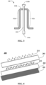
- FIGS. 1-3 a calibration circuit board 100 according to some embodiments of the present disclosure is described in detail. It should be noted that other components may be present in the actual calibration circuit board that are not shown in the drawings and discussed herein in order to avoid obscuring the gist of the present disclosure.
- the calibration circuit board 100 may include a first metal layer 101, a first substrate 102, and a second substrate 103.
- the first metal layer 101 is configured to be grounded (i.e., attached to a ground reference voltage).
- the first substrate 102 is disposed over the first metal layer 101.
- the second substrate 103 is disposed over the first substrate 102.
- the calibration circuit board 100 may include a plurality of couplers.
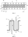
- FIG. 2 schematically illustrates that the calibration circuit board 100 includes 16 couplers 110-1, 110-2, 110-3, ..., 110-16, but this is merely an example and is not intended to limit the present disclosure.
- the calibration circuit board 100 may be provided with more or fewer couplers according to actual needs.
- the number of couplers included in the calibration circuit board 100 may depend on the specific number of ports and/or radiating units in the antenna array to which it is applied.
- couplers 110-1, 110-2, 110-3, ..., 110-16 may be collectively referred to as "couplers 110".
- the plurality of couplers 110 may have individual transmission lines 111 and serially connected coupling lines 112. As can be seen in FIGS. 1 and 2 , the coupling lines 112 of the plurality of couplers 110 are connected in series with each other.
- a first end of the first coupler 110-1 acts as a first calibration port 120a and a second end of the last coupler 110-16 acts as a second calibration port 120b.
- the first calibration port 120a and the second calibration port 120b are capable of providing outputs independently of each other.
- the calibration circuit board 100 can have the following ability: when a signal is input to the input port of any one of the couplers 110, coupled components of the input signal can be obtained at both the first calibration port 120a and the second calibration port 120b.
- the two coupled components are obtained by coupling and transferring the input signal through two different paths, where each path is independent of the other path.
- the amplitude/phase consistency between the transmitting channels may be determined by comparing the outputs of the first calibration port 120a and the second calibration port 120b.
- the particular calibration algorithm may employ any suitable algorithm known or later developed in the art without particular limitation by the present disclosure.
- the two calibration ports 120a and 120b, independent of each other, can be used to eliminate channel differences introduced by the calibration board itself, thereby more accurately detecting amplitude/phase inconsistencies caused by the transmitting/receiving channels.
- the transmission lines 111 and the coupling lines 112 of the plurality of couplers 110 may be disposed in different layers. One of the transmission lines 111 and the coupling lines 112 of the plurality of couplers 110 may be disposed between the first substrate 102 and the second substrate 103, and the other of the transmission lines 111 and the coupling lines 112 of the plurality of couplers 110 may be disposed over the second substrate 103. In the non-limiting example shown in FIG. 1 , the coupling lines 112 of the plurality of couplers 110 of the calibration circuit board 100 are disposed between the first substrate 102 and the second substrate 103, and the transmission lines 111 of the plurality of couplers 110 are disposed over the second substrate 103.
- the calibration circuit board may have a more compact arrangement.
- the area of the calibration circuit board 100 can be reduced by 40% compared to a conventional 16-port series calibration circuit board.
- Calibration signals may be coupled from the transmission lines 111 to the coupling lines 112 of the couplers through the second substrate 103.
- the first metal layer 101 may take the form of a metal plate. In some embodiments, the first metal layer 101 may be deposited on the lower surface of the first substrate 102, for example, by electroplating. In some embodiments, the first and second substrates 102, 103 may take the form of dielectric plates. In some embodiments, the thickness of the second substrate 103 may be between 20 mil and 40 mil (e.g., 30 mil). The thickness of the second substrate 103 may be specifically set in consideration of the required coupling strength between the transmission line and the coupling line, and the like.
- the transmission line 111 and the coupling line 112 may be any one of a coaxial line, a rectangular waveguide, a circular waveguide, a strip line, a microstrip line, and other transmission lines.
- the transmission lines 111 and the coupling lines 112 may be formed of a conductive material.
- the transmission lines 111 and the coupling lines 112 may be made of a metal such as copper.
- the transmission lines 111 and the coupling lines 112 may be made of a metal foil such as a copper foil, and the coupling lines 112 disposed between the first substrate 102 and the second substrate 103 may be bonded (e.g., by adhesion, etc.) to the upper surface of the first substrate 102 and the lower surface of the second substrate 103 simultaneously, while the transmission lines 111 disposed over the second substrate 103 may be bonded (e.g., by adhesion, etc.) to the upper surface of the second substrate 103.
- the first substrate 102 may be a double-sided metal-bonded dielectric substrate, for example, a double-sided copper-bonded dielectric substrate.
- the lower surface of the double-sided metal-bonded dielectric substrate 102 may be considered as the first metal layer 101 of the calibration circuit board 100 for grounding, and the metal on the upper surface of the double-sided metal-bonded dielectric substrate 102 may be etched to form the coupling lines 112.
- the second substrate 103 may be a double-sided metal-bonded dielectric substrate, for example, a double-sided copper-bonded dielectric substrate.
- the metal on the lower surface of the double-sided metal-bonded dielectric substrate 103 may be etched to form the coupling lines 112, and the metal on the upper surface of the double-sided metal-bonded dielectric substrate 103 may be etched to form the transmission lines 111.
- the transmission lines and the coupling lines of the plurality of couplers may be metal traces formed on upper and lower sides of the second substrate, respectively. In the embodiments in which the transmission lines and the coupling lines are formed on different surfaces of the second substrate, respectively, when a main functional component of the calibration circuit board 100, such as a coupler, fails, only the second substrate may be replaced without replacing the first substrate and the first metal layer, thereby facilitating repair and/or maintenance and saving costs.
- Each coupler 110 may include a transmission line 111 and a coupling line 112.
- An input port 111a and an output port 111b are provided at respective ends of the transmission line 111.
- the transmission line 111 may be used to transmit signals between the respective radio frequency port and the respective radiating unit.
- the input port 111a may be used to receive an RF signal, for example from a beam forming network or other feed network, which is then passed to the corresponding radiating unit via the output port 111b.
- the coupling line 112 is coupled to the transmission line 111, and includes two first portions (which may also be referred to as coupling portions) 112a and 112c respectively located at both sides of the transmission line 111 as viewed from a direction perpendicular to the calibration circuit board, and a second portion (which may also be referred to as a connecting portion) 112b connected between the two first portions 112a and 112c.
- the coupling between the transmission line 111 and the first portions 112a, 112c of the coupling line 112 may be achieved by various known coupling techniques.
- the transmission line 111 may be parallel to the first portions 112a, 112c of the coupling line 112, respectively, so that the coupling between the transmission line 111 and the first portions 112a, 112c of the coupling line 112 may be achieved by means of parallel coupling through the substrate 103.
- the transmission lines 111 of the respective ones of the plurality of couplers are parallel to each other, and the two first portions 112a, 112c of the coupling line 112 of each of the plurality of couplers 110 are coupled in parallel to the transmission line 111 of that coupler 110.
- the coupling lines 112 of the plurality of couplers 110 may collectively form a continuous line.
- the transmission lines 111 of the plurality of couplers 110 are parallel to each other, and the coupling lines 112 of the plurality of couplers 110 may collectively form one continuous serpentine line having a plurality of parallel line segments (serving as coupling portions) that are parallel to each other and parallel to the transmission lines 111 and a plurality of connecting line segments 112b (serving as connecting portions) that connect the plurality of parallel line segments end to end, and two adjacent parallel line segments may be coupled in parallel to each respective transmission line thereabove to form a coupler.
- the transmission line 111 of each of the plurality of couplers 110 is in the middle of the two first portions of the coupling line 112 of that coupler 110.
- the transmission line 111 may be located at an intermediate position between the first portions 112a, 112c of the coupling line 112, as viewed from a direction perpendicular to the calibration circuit board 100.
- the transmission lines 111 of the plurality of couplers 110 extend beyond a region where the coupling lines 112 of the plurality of couplers 110 are present, as seen in a direction perpendicular to the calibration circuit board 100.
- the effective coupling length L of the transmission line 111 and the coupling lines 112 of the coupler 110 may be a projected length of the transmission line 111 on the first portion of the coupling line 112. In some embodiments, the effective coupling length L of the coupler 110 may be equal to a quarter wavelength of a radio frequency signal provided to the transmission line 111 of that coupler 110. In the example shown in FIG. 2 , the effective coupling length L of the transmission line 111 and the coupling line 112 of the coupler 110 is the length of the first portion of the coupling line 112. In some embodiments, a length of the first portion of the coupling line of each of the plurality of couplers 110 is equal to a quarter wavelength of an RF signal provided to the transmission line 111 of that coupler 110.
- the lengths of the first portions 112a, 112c of the coupling line 112 may be set to a quarter wavelength of an RF signal input at the input port 111a to the transmission line 111.
- the effective coupling length L may be less than the length of the first portion of the coupling line 112. It will be appreciated that the effective coupling length L of the coupler 110 may be set according to specific requirements on the coupling strength of the coupler, etc.
- the shape of the second portion 112b is not particularly limited. In some embodiments, a length of the second portion 112b may be designed to meet impedance matching requirements. In some examples, the length of the second portion 112b is designed to provide an impedance of 50 ohms.
- the main energy of the coupled component obtained at the first portion 112a of the coupling line of the coupler 110-2 passes through the coupling line of the coupler 110-1 to the first calibration port 120a in this order, and the main energy of the coupled component obtained at the first portion 112c of the coupling line of the coupler 110-2 passes through the coupling lines of the couplers 110-3 to 110-16 in this order to the second calibration port 120b. It is not necessary to ensure that the respective couplers 110 have identical circuit structures, since the difference in the circuit structures can be eliminated in the calibration algorithm based on the two coupled components at the first calibration port 120a and the second calibration port 120b.
- all input ports and all output ports of the transmission lines of the plurality of couplers are respectively located at the same side with respect to the region where the coupling lines of the plurality of couplers are present.
- all of the input ports of the transmission lines of the plurality of couplers are near the upper side of FIG. 2 and all of the output ports are near the lower side of FIG. 2 . This has the advantage that the input ports and the output ports are concentrated on one side of the substrate, respectively, for easy connection to other assemblies.
- a first portion of a coupling line of at least one of the plurality of couplers 110 has a common portion with a first portion of a coupling line of an adjacent coupler of the plurality of couplers.
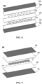
- FIGS. 4-6 illustrate a calibration circuit board 200 according to some embodiments of the present disclosure.
- the calibration circuit board 200 is different from the calibration circuit board 100 in that the first portions of the coupling line of a coupler of the plurality of couplers of the calibration circuit board 200 have common portions with the first portions of the coupling lines of adjacent couplers of the plurality of couplers, and except for this, the calibration circuit board 200 may have substantially the same configuration as the calibration circuit board 100, and thus the above discussion about the calibration circuit board 100 is also applicable to the calibration circuit board 200, which is not repeated herein.
- the calibration circuit board 200 may include a first metal layer 201, a first substrate 202 disposed over the first metal layer 201, and a second substrate 203 disposed over the first substrate 202.
- the calibration circuit board 200 may further include coupling lines 212 disposed between the first substrate 202 and the second substrate 203 and transmission lines 211 disposed over the second substrate 203.
- the calibration circuit board 200 includes a plurality of couplers 210-1, 210-2, 210-3, ..., 210-16 (also sometimes referred to hereinafter collectively as couplers 210).
- the coupling lines of the plurality of couplers 210 are connected in series to provide two independent calibration ports 220a and 220b.
- the first portions of the coupling lines of adjacent ones of the plurality of couplers of the calibration circuit board 200 have common portions.
- the adjacent couplers 210-1 and 210-2 are illustrated as examples.
- the coupler 210-1 includes a transmission line 211-1, at both ends of which an input port 211-1a and an output port 211-1b are provided, respectively, and the coupler 210-2 includes a transmission line 211-2, at both ends of which an input port 211-2a and an output port 211-2b are provided, respectively.
- the coupling line of the coupler 210-1 includes two first portions 212a, 212c respectively located at both sides of the transmission line 211-1 thereof as viewed in a direction perpendicular to the calibration circuit board 200 and a second portion 212b connected between the two first portions 212a, 212c
- the coupling line of the coupler 210-2 includes two first portions 212c, 212e respectively located at both sides of the transmission line 211-2 thereof as viewed in a direction perpendicular to the calibration circuit board 200 and a second portion 212d connected between the two first portions 212c, 212e.
- the coupler 210-1 and the coupler 210-2 share the first portion 212c. As shown in FIG.
- a plurality of couplers 210 share the serially connected coupling lines in a manner similar to that shown in FIG. 6 . Since there is a common portion between the first portions of the coupling lines of adjacent couplers, the arrangement among the couplers can be more compact, reducing the size of the calibration circuit board, and in addition, since the path from the input port of the coupler to the calibration port is shortened, the insertion loss of the calibration port with respect to the input port is also reduced.
- the calibration circuit board according to the present disclosure may further include: a third substrate disposed over the second substrate such that one of the transmission lines and the coupling lines of the plurality of couplers disposed over the second substrate is located between the second substrate and the third substrate; and a second metal layer disposed over the third substrate and configured to be grounded.
- the calibration circuit board 100' as shown in FIG. 7 further includes a third substrate 104 disposed over the second substrate 103 and a second metal layer 105 disposed over the third substrate 104, in which the transmission lines 111 are disposed between the second substrate 103 and the third substrate 104.
- the calibration circuit board 200' shown in FIG. 8 further includes a third substrate 204 disposed over the second substrate 203 and a second metal layer 205 disposed over the third substrate 204, in which the transmission lines 211 are disposed between the second substrate 203 and the third substrate 204.
- the third substrate 104, 204 may be similar to the first substrate and the second substrate as described above, and the second metal layer 105, 205 may be similar to the first metal layer as described above, which will not be described herein again.
- the closed design of the calibration circuit boards 100', 200' is more resistant to external interference than an open design of the calibration circuit boards 100, 200 where the transmission lines are exposed to the outside, especially when the frequencies of the signals increase, which reduces amplitude/phase fluctuations of the signals.
- the calibration circuit board may be implemented as a multilayer printed circuit board.
- the calibration circuit board may be implemented to include three separate boards, wherein a first board may include a first metal layer and a first substrate, a second board may include coupling lines, a second substrate, and transmission lines, and a third board may include a third substrate and a second metal layer.
- the first board and the third board may be dielectric plates with metal layers deposited on their surfaces, and the second board may be a dielectric plate with metal lines formed on its upper and lower sides.
- a main functional component of the calibration circuit board such as a coupler, fails, only the second board may be replaced without replacing the first board and the third board, thereby facilitating repair and/or maintenance and saving costs.
- the calibration circuit board including the third substrate may not include the second substrate, such that the transmission lines and the coupling lines of the plurality of couplers are collectively disposed between the first substrate and the third substrate.
- the calibration circuit board 300 differs from the calibration circuit board 200' in that it does not include the second substrate 203.
- the calibration circuit board 300 includes a first metal layer 301, a first substrate 302 disposed over the first metal layer 301, a third substrate 304 disposed over the first substrate 302, and a second metal layer 305 disposed over the third substrate 304.
- the transmission lines 311 and the coupling lines 312 of the plurality of couplers are commonly disposed between the first substrate 302 and the third substrate 304.
- Such a closed design is resistant to external interference, especially when the frequencies of the signals increase, thereby reducing amplitude/phase fluctuations of the signals.
- an antenna apparatus comprising: a plurality of radiating units; a plurality of RF ports; and the calibration circuit board according to any embodiment of the present disclosure, wherein the input port of each coupler of the calibration circuit board is connected to a respective one of the plurality of RF ports, and the output port of each coupler of the calibration circuit board is connected to a respective one of the plurality of radiating units.
- An antenna apparatus 400 according to some embodiments of the present disclosure is now described with reference to FIG. 10 . It should be noted that other components may be present in an actual antenna apparatus, and are not shown in the drawings and discussed herein in order to avoid obscuring the gist of the present disclosure.
- the antenna apparatus 400 may comprise an RF processing module 401, a calibration circuit board 402 and an antenna array 403.
- the antenna array 403 may comprise a plurality of radiating units 403-1, 403-2, ..., 403-n (n is a positive integer), each radiating unit may comprise a radiating element or a vertically arranged column of multiple radiating elements.
- the RF processing module 401 may generally comprise an antenna interface unit, an RF transceiver, a beam forming network, and the like.
- the antenna interface unit may receive a signal to be transmitted from a baseband unit, divide the signal into a number of identical sub-components (e.g., the number of sub-components may be equal to the number of radiating units 403-1, 403-2, ..., 403-n), and apply a predetermined gain and phase to each sub-component, and then provide the respective sub-components to the corresponding RF transceiver.
- the individual sub-components of the signal are converted to analog signals at the RF transceiver and then reach the corresponding radiating units via the beam forming network.
- the signals radiated from the radiating units are interferometrically superimposed to form a desired beam pattern.
- the RF processing module 401 provides a plurality of RF ports 401-1, 401-2, ..., 401-n (n is a positive integer) for providing signals to the plurality of radiating units 403-1, 403-2, ..., 403-n, respectively.
- the calibration circuit board 402 may be the calibration circuit board according to any embodiment of the present disclosure, which may be disposed between the RF processing module 401 and the antenna array 403.
- the calibration circuit board 402 may comprise a plurality of couplers 402-1, 402-2, ..., 402-n (n is a positive integer).
- the coupling lines of the plurality of couplers 402-1, 402-2, ..., 402-n are connected in series with each other (not specifically depicted in FIG. 10 ).
- the input ports 402-1a, 402-2a, ..., 402-na of the respective couplers 402-1, 402-2, ..., 402-n of the calibration circuit board 402 may be connected to respective ones of the plurality of RF ports 401-1, 401-2, ..., 401-n, and the output ports 402-1b, 402-2b, ..., 402-nb of the respective couplers 402-1, 402-2, ..., 402-n of the calibration circuit board may be connected to respective ones of the plurality of radiating units 403-1, 403-2, ..., 403-n.
- calibration test signals are transmitted from the RF ports 401-1, 401-2, ..., 401-n to the radiating units 403-1, 403-2, ..., 403-n.
- a portion of the power of the calibration test signal transmitted on the transmitting channels is extracted via the couplers 402-1, 402-2, ..., 402-n of the calibration circuit board 402 and output from the calibration ports of the calibration circuit board.
- the gains and phases of all the transmitting/receiving channels of the antenna apparatus 400 can be accurately monitored and adjusted so that a desired beam pattern can be formed.
- the antenna apparatus 400 according to the embodiments of the present disclosure can realize more ports while having a small size, thereby meeting the requirements of high integration and miniaturization of the antenna.
- an element described as being “over,” “attached to,” “connected to,” “coupled to,” or “contacting” another element or the like may be directly over, directly attached to, directly connected to, directly coupled to or directly contact the other element, or one or more intermediate elements may be present.
- one feature may be arranged to be “adjacent to” another feature, which may mean that the one feature has a portion that overlaps with the adjacent feature or has a portion above or below the adjacent feature.
- the term "exemplary” means “serving as an example, instance, or illustration,” and not as a “model” that is to be reproduced exactly. Any implementation exemplarily described herein is not necessarily to be construed as preferred or advantageous over other implementations. Furthermore, the present disclosure is not restricted by any expressed or implied theory presented in the technical field, background, summary of the invention, or detailed description.
- the term “substantially” is intended to encompass any minor variations due to design or manufacturing imperfections, tolerances of the devices or elements, environmental influences and/or other factors.
- the term “substantially” also allows for differences from a perfect or ideal situation due to parasitic effect, noise, and other practical considerations that may exist in a practical implementation.
- first,” “second,” and the like may also be used herein for reference purposes only, and thus are not intended to be limiting.
- the terms “first,” “second,” and other such numerical terms referring to structures or elements do not imply a sequence or order unless clearly indicated by the context.
- providing is used broadly to encompass all ways of obtaining an object, and thus “providing an object” includes, but is not limited to, “purchasing,” “preparing/manufacturing,” “arranging/setting,” “installing/assembling,” and/or “ordering” the object, and the like.
Landscapes
- Engineering & Computer Science (AREA)
- Microelectronics & Electronic Packaging (AREA)
- Physics & Mathematics (AREA)
- Electromagnetism (AREA)
- Computer Networks & Wireless Communication (AREA)
- Signal Processing (AREA)
- Variable-Direction Aerials And Aerial Arrays (AREA)
- Transceivers (AREA)
Claims (13)
- Carte de circuit d'étalonnage (100, 200, 100', 200', 402) pour une antenne, comprenant :une première couche métallique (101, 201) ;un premier substrat (102, 202) sur la première couche métallique (101, 201) ;un deuxième substrat (103, 203) sur le premier substrat (102, 202) ; etune pluralité de coupleurs (110, 210), chaque coupleur comprenant :une ligne de transmission (111, 211) pourvue d'un port d'entrée (111a, 211-1a, 211-2a) et d'un port de sortie (111b, 211-1b, 211-2b) à leurs extrémités respectives ; etune ligne de couplage (112, 212) couplée à la ligne de transmission (111, 211) et comprenant deux premières portions (112a, 112c, 212a, 212c, 212c, 212e) situées respectivement des deux côtés de la ligne de transmission (111, 211), telles que vues depuis une direction perpendiculaire à la carte de circuit d'étalonnage, et une deuxième portion (112b, 212b, 212d) connectée entre les deux premières portions,dans laquelle les lignes de couplage (112, 212) de la pluralité de coupleurs (110, 210) sont connectées en série pour fournir un premier port d'étalonnage (120a) et un deuxième port d'étalonnage (120b),dans laquelle les unes parmi les lignes de transmission (111, 211) et les lignes de couplage (112, 212) de la pluralité de coupleurs (110, 210) sont entre le premier substrat (102, 202) et le deuxième substrat (103, 203), et les autres parmi les lignes de transmission (111, 211) et les lignes de couplage (112, 212) de la pluralité de coupleurs (110, 210) sont sur le deuxième substrat (103, 203).
- Carte de circuit d'étalonnage selon la revendication 1, dans laquelle les lignes de couplage (112, 212) de la pluralité de coupleurs (110, 210) sont entre le premier substrat (102, 202) et le deuxième substrat (103, 203), et les lignes de transmission (111, 211) de la pluralité de coupleurs (110, 210) sont sur le deuxième substrat (103, 203).
- Carte de circuit d'étalonnage selon la revendication 1 ou la revendication 2, dans laquelle une première portion d'une ligne de couplage de l'au moins un parmi la pluralité de coupleurs (110, 210) a une portion commune avec une première portion d'une ligne de couplage d'un coupleur adjacent de la pluralité de coupleurs (110, 210).
- Carte de circuit d'étalonnage selon l'une quelconque des revendications 1 à 3, dans laquelle les lignes de transmission (111, 211) des coupleurs respectifs parmi la pluralité de coupleurs (110, 210) sont parallèles les unes par rapport aux autres, et les deux premières portions (112a, 112c, 212a, 212c, 212c, 212e) de la ligne de couplage (112, 212) de chacun de la pluralité de coupleurs (110, 210) sont couplées parallèlement à la ligne de transmission (111, 211) de ce coupleur.
- Carte de circuit d'étalonnage selon l'une quelconque des revendications 1 à 4, dans laquelle la ligne de transmission (111, 211) de chacun de la pluralité de coupleurs (110, 210) est entre les deux premières portions (112a, 112c, 212a, 212c, 212c, 212e) de la ligne de couplage (112, 212) de ce coupleur.
- Carte de circuit d'étalonnage selon l'une quelconque des revendications 1 à 5, dans laquelle la carte de circuit d'étalonnage (100, 200, 100', 200', 402) est configurée pour fonctionner sur des signaux de fréquence radio dans une première bande de fréquence, et dans laquelle une longueur de l'au moins une parmi les premières portions de la ligne de couplage (112, 212) de chacun de la pluralité de coupleurs (110, 210) est égale à un quart de longueur d'onde d'une fréquence centrale de la première bande radiofréquence.
- Carte de circuit d'étalonnage selon l'une quelconque des revendications 1 à 6, dans laquelle une longueur de la deuxième portion (112b, 212b, 212d) de la ligne de couplage (112, 212) de chacun de la pluralité de coupleurs (110, 210) est configurée pour satisfaire aux exigences d'adaptation d'impédance.
- Carte de circuit d'étalonnage selon l'une quelconque des revendications 1 à 7, dans laquelle les lignes de transmission (111, 211) de la pluralité de coupleurs (110, 210) s'étendent, vues dans la direction perpendiculaire à la carte de circuit d'étalonnage, au-delà d'une région où les lignes de couplage (112, 212) de la pluralité de coupleurs (110, 210) sont présentes.
- Carte de circuit d'étalonnage selon l'une quelconque des revendications 1 à 8, dans laquelle tous les ports d'entrée (111a, 211-1a, 211-2a) des lignes de transmission (111, 211) de la pluralité de coupleurs (110, 210) sont respectivement situés d'un premier côté d'une région où les lignes de couplage (112, 212) de la pluralité de coupleurs (110, 210) sont présentes, et dans laquelle tous les ports de sortie (111b, 211-1b, 211-2b) des lignes de transmission (111, 211) de la pluralité de coupleurs (110, 210) sont respectivement situés d'un deuxième côté de la région où les lignes de couplage (112, 212) de la pluralité de coupleurs (110, 210) sont présentes.
- Carte de circuit d'étalonnage selon l'une quelconque des revendications 1 à 9, comprenant en outre :un troisième substrat (104, 204) sur le deuxième substrat (103, 203) de telle sorte que les autres parmi les lignes de transmission (111, 211) et les lignes de couplage (112, 212) de la pluralité de coupleurs (110, 210) sont situées entre le deuxième substrat (103, 203) et le troisième substrat (104, 204) ; etune deuxième couche métallique (105, 205) sur le troisième substrat (104, 204).
- Carte de circuit d'étalonnage selon l'une quelconque des revendications 1 à 10, dans laquelle la carte de circuit d'étalonnage est mise en oeuvre sous la forme d'une carte de circuit imprimé multicouche.
- Carte de circuit d'étalonnage selon l'une quelconque des revendications 1 à 11, dans laquelle les lignes de transmission (111, 211) et les lignes de couplage (112, 212) de la pluralité de coupleurs (110, 210) sont des pistes métalliques formées sur les côtés supérieur et inférieur du deuxième substrat, respectivement.
- Appareil d'antenne (400), comprenant :une pluralité d'unités rayonnantes (403-1, 403-2, ..., 403-n) ;une pluralité de ports radiofréquence ; etla carte de circuit d'étalonnage selon l'une quelconque des revendications 1 à 12, dans lequel le port d'entrée de chaque coupleur (110, 210) de la carte de circuit d'étalonnage est connecté à l'un respectif de la pluralité de ports radiofréquence, et le port de sortie de chaque coupleur (110, 210) de la carte de circuit d'étalonnage est connecté à l'une respective de la pluralité d'unités rayonnantes.
Applications Claiming Priority (1)
| Application Number | Priority Date | Filing Date | Title |
|---|---|---|---|
| CN202010472391.2A CN113745820B (zh) | 2020-05-29 | 2020-05-29 | 校准电路板及包含该校准电路板的天线装置 |
Publications (2)
| Publication Number | Publication Date |
|---|---|
| EP3916914A1 EP3916914A1 (fr) | 2021-12-01 |
| EP3916914B1 true EP3916914B1 (fr) | 2025-01-15 |
Family
ID=76034515
Family Applications (1)
| Application Number | Title | Priority Date | Filing Date |
|---|---|---|---|
| EP21174965.0A Active EP3916914B1 (fr) | 2020-05-29 | 2021-05-20 | Carte de circuit d'étalonnage et appareil d'antenne la comprenant |
Country Status (4)
| Country | Link |
|---|---|
| US (1) | US11985761B2 (fr) |
| EP (1) | EP3916914B1 (fr) |
| CN (1) | CN113745820B (fr) |
| FI (1) | FI3916914T3 (fr) |
Families Citing this family (4)
| Publication number | Priority date | Publication date | Assignee | Title |
|---|---|---|---|---|
| CN111525220B (zh) * | 2019-02-01 | 2022-12-30 | 康普技术有限责任公司 | 耦合装置及天线 |
| CN114512805B (zh) * | 2022-01-19 | 2023-08-25 | 中国电子科技集团公司第十研究所 | 埋藏式夹心宽带耦合校准网络 |
| CN115275555B (zh) * | 2022-08-05 | 2023-11-10 | 中国船舶集团有限公司第七二三研究所 | 一种集成于天线的超宽带定向耦合器 |
| CN119487697A (zh) | 2022-08-08 | 2025-02-18 | 户外无线网络有限公司 | 混合耦合器和用于制造混合耦合器的方法 |
Family Cites Families (6)
| Publication number | Priority date | Publication date | Assignee | Title |
|---|---|---|---|---|
| US6356233B1 (en) * | 2000-12-12 | 2002-03-12 | Lockheed Martin Corporation | Structure for an array antenna, and calibration method therefor |
| JP6660892B2 (ja) * | 2014-06-12 | 2020-03-11 | スカイワークス ソリューションズ, インコーポレイテッドSkyworks Solutions, Inc. | 方向性結合器に関連するデバイスおよび方法 |
| CN105390814B (zh) * | 2015-10-18 | 2018-06-26 | 中国电子科技集团公司第十研究所 | 具有内校准网络的有源相控阵天线 |
| CN110557206B (zh) * | 2018-05-31 | 2022-09-06 | 康普技术有限责任公司 | 天线校准装置 |
| CN111147159B (zh) * | 2019-12-31 | 2025-05-27 | 京信通信技术(广州)有限公司 | 校准电路、校准网络和智能天线 |
| CN211980895U (zh) * | 2020-05-29 | 2020-11-20 | 康普技术有限责任公司 | 校准电路板及包含该校准电路板的天线装置 |
-
2020
- 2020-05-29 CN CN202010472391.2A patent/CN113745820B/zh active Active
-
2021
- 2021-05-12 US US17/318,514 patent/US11985761B2/en active Active
- 2021-05-20 FI FIEP21174965.0T patent/FI3916914T3/fi active
- 2021-05-20 EP EP21174965.0A patent/EP3916914B1/fr active Active
Also Published As
| Publication number | Publication date |
|---|---|
| EP3916914A1 (fr) | 2021-12-01 |
| FI3916914T3 (fi) | 2025-03-12 |
| CN113745820B (zh) | 2025-12-05 |
| US20210378091A1 (en) | 2021-12-02 |
| CN113745820A (zh) | 2021-12-03 |
| US11985761B2 (en) | 2024-05-14 |
Similar Documents
| Publication | Publication Date | Title |
|---|---|---|
| EP3916914B1 (fr) | Carte de circuit d'étalonnage et appareil d'antenne la comprenant | |
| US10797408B1 (en) | Antenna structure and method for manufacturing the same | |
| US10333228B2 (en) | Low coupling 2×2 MIMO array | |
| EP3826105B1 (fr) | Système d'antennes et station de base | |
| WO2015109706A1 (fr) | Unité d'antenne et terminal | |
| US11705614B2 (en) | Coupling device and antenna | |
| US12294141B2 (en) | Antenna calibration boards having non-uniform coupler sections | |
| CN112242612A (zh) | 贴片天线 | |
| KR20140118388A (ko) | 안테나 장치 및 그를 구비하는 전자 기기 | |
| US11968782B2 (en) | Coupler and base station antenna | |
| EP4136758B1 (fr) | Agencement d'émetteur, émetteur-récepteur, système de communication radio et procédé | |
| CN211980895U (zh) | 校准电路板及包含该校准电路板的天线装置 | |
| EP4290688A1 (fr) | Ensembles antennes et modules d'antennes destinés à être utilisés dans des systèmes de communication sans fil | |
| CN110416706B (zh) | 用于波束成形天线和相关基站天线的校准电路 | |
| EP4128548B1 (fr) | Groupement d'antennes réseau | |
| EP1168493B1 (fr) | Antenne à deux polarisations | |
| WO2023091876A1 (fr) | Antennes de station de base comprenant un circuit d'alimentation et un circuit d'étalonnage qui partagent une carte | |
| WO2024050198A1 (fr) | Antenne de station de base | |
| WO2020253938A1 (fr) | Structure d'antenne à orientation de faisceau continu | |
| KR102722676B1 (ko) | 다중 대역 방사체 모듈 | |
| CN117199778A (zh) | 用于无线通信系统的天线组件和天线模块 | |
| EP3582326B1 (fr) | Couplage d'antenne |
Legal Events
| Date | Code | Title | Description |
|---|---|---|---|
| PUAI | Public reference made under article 153(3) epc to a published international application that has entered the european phase |
Free format text: ORIGINAL CODE: 0009012 |
|
| STAA | Information on the status of an ep patent application or granted ep patent |
Free format text: STATUS: REQUEST FOR EXAMINATION WAS MADE |
|
| 17P | Request for examination filed |
Effective date: 20210520 |
|
| AK | Designated contracting states |
Kind code of ref document: A1 Designated state(s): AL AT BE BG CH CY CZ DE DK EE ES FI FR GB GR HR HU IE IS IT LI LT LU LV MC MK MT NL NO PL PT RO RS SE SI SK SM TR |
|
| B565 | Issuance of search results under rule 164(2) epc |
Effective date: 20211028 |
|
| STAA | Information on the status of an ep patent application or granted ep patent |
Free format text: STATUS: EXAMINATION IS IN PROGRESS |
|
| 17Q | First examination report despatched |
Effective date: 20230301 |
|
| RAP3 | Party data changed (applicant data changed or rights of an application transferred) |
Owner name: COMMSCOPE TECHNOLOGIES LLC |
|
| RAP1 | Party data changed (applicant data changed or rights of an application transferred) |
Owner name: OUTDOOR WIRELESS NETWORKS LLC |
|
| GRAP | Despatch of communication of intention to grant a patent |
Free format text: ORIGINAL CODE: EPIDOSNIGR1 |
|
| STAA | Information on the status of an ep patent application or granted ep patent |
Free format text: STATUS: GRANT OF PATENT IS INTENDED |
|
| INTG | Intention to grant announced |
Effective date: 20241009 |
|
| GRAS | Grant fee paid |
Free format text: ORIGINAL CODE: EPIDOSNIGR3 |
|
| GRAA | (expected) grant |
Free format text: ORIGINAL CODE: 0009210 |
|
| STAA | Information on the status of an ep patent application or granted ep patent |
Free format text: STATUS: THE PATENT HAS BEEN GRANTED |
|
| AK | Designated contracting states |
Kind code of ref document: B1 Designated state(s): AL AT BE BG CH CY CZ DE DK EE ES FI FR GB GR HR HU IE IS IT LI LT LU LV MC MK MT NL NO PL PT RO RS SE SI SK SM TR |
|
| REG | Reference to a national code |
Ref country code: CH Ref legal event code: EP Ref country code: GB Ref legal event code: FG4D |
|
| REG | Reference to a national code |
Ref country code: DE Ref legal event code: R096 Ref document number: 602021024871 Country of ref document: DE |
|
| REG | Reference to a national code |
Ref country code: IE Ref legal event code: FG4D |
|
| REG | Reference to a national code |
Ref country code: FI Ref legal event code: FGE |
|
| REG | Reference to a national code |
Ref country code: SE Ref legal event code: TRGR |
|
| REG | Reference to a national code |
Ref country code: NL Ref legal event code: MP Effective date: 20250115 |
|
| PG25 | Lapsed in a contracting state [announced via postgrant information from national office to epo] |
Ref country code: NL Free format text: LAPSE BECAUSE OF FAILURE TO SUBMIT A TRANSLATION OF THE DESCRIPTION OR TO PAY THE FEE WITHIN THE PRESCRIBED TIME-LIMIT Effective date: 20250115 |
|
| PG25 | Lapsed in a contracting state [announced via postgrant information from national office to epo] |
Ref country code: RS Free format text: LAPSE BECAUSE OF FAILURE TO SUBMIT A TRANSLATION OF THE DESCRIPTION OR TO PAY THE FEE WITHIN THE PRESCRIBED TIME-LIMIT Effective date: 20250415 |
|
| PGFP | Annual fee paid to national office [announced via postgrant information from national office to epo] |
Ref country code: FI Payment date: 20250526 Year of fee payment: 5 |
|
| PG25 | Lapsed in a contracting state [announced via postgrant information from national office to epo] |
Ref country code: PL Free format text: LAPSE BECAUSE OF FAILURE TO SUBMIT A TRANSLATION OF THE DESCRIPTION OR TO PAY THE FEE WITHIN THE PRESCRIBED TIME-LIMIT Effective date: 20250115 |
|
| PG25 | Lapsed in a contracting state [announced via postgrant information from national office to epo] |
Ref country code: ES Free format text: LAPSE BECAUSE OF FAILURE TO SUBMIT A TRANSLATION OF THE DESCRIPTION OR TO PAY THE FEE WITHIN THE PRESCRIBED TIME-LIMIT Effective date: 20250115 |
|
| REG | Reference to a national code |
Ref country code: LT Ref legal event code: MG9D |
|
| PG25 | Lapsed in a contracting state [announced via postgrant information from national office to epo] |
Ref country code: IS Free format text: LAPSE BECAUSE OF FAILURE TO SUBMIT A TRANSLATION OF THE DESCRIPTION OR TO PAY THE FEE WITHIN THE PRESCRIBED TIME-LIMIT Effective date: 20250515 Ref country code: NO Free format text: LAPSE BECAUSE OF FAILURE TO SUBMIT A TRANSLATION OF THE DESCRIPTION OR TO PAY THE FEE WITHIN THE PRESCRIBED TIME-LIMIT Effective date: 20250415 |
|
| REG | Reference to a national code |
Ref country code: AT Ref legal event code: MK05 Ref document number: 1760449 Country of ref document: AT Kind code of ref document: T Effective date: 20250115 |
|
| PG25 | Lapsed in a contracting state [announced via postgrant information from national office to epo] |
Ref country code: HR Free format text: LAPSE BECAUSE OF FAILURE TO SUBMIT A TRANSLATION OF THE DESCRIPTION OR TO PAY THE FEE WITHIN THE PRESCRIBED TIME-LIMIT Effective date: 20250115 |
|
| PG25 | Lapsed in a contracting state [announced via postgrant information from national office to epo] |
Ref country code: PT Free format text: LAPSE BECAUSE OF FAILURE TO SUBMIT A TRANSLATION OF THE DESCRIPTION OR TO PAY THE FEE WITHIN THE PRESCRIBED TIME-LIMIT Effective date: 20250515 Ref country code: LV Free format text: LAPSE BECAUSE OF FAILURE TO SUBMIT A TRANSLATION OF THE DESCRIPTION OR TO PAY THE FEE WITHIN THE PRESCRIBED TIME-LIMIT Effective date: 20250115 |
|
| PG25 | Lapsed in a contracting state [announced via postgrant information from national office to epo] |
Ref country code: GR Free format text: LAPSE BECAUSE OF FAILURE TO SUBMIT A TRANSLATION OF THE DESCRIPTION OR TO PAY THE FEE WITHIN THE PRESCRIBED TIME-LIMIT Effective date: 20250416 Ref country code: BG Free format text: LAPSE BECAUSE OF FAILURE TO SUBMIT A TRANSLATION OF THE DESCRIPTION OR TO PAY THE FEE WITHIN THE PRESCRIBED TIME-LIMIT Effective date: 20250115 |
|
| PG25 | Lapsed in a contracting state [announced via postgrant information from national office to epo] |
Ref country code: AT Free format text: LAPSE BECAUSE OF FAILURE TO SUBMIT A TRANSLATION OF THE DESCRIPTION OR TO PAY THE FEE WITHIN THE PRESCRIBED TIME-LIMIT Effective date: 20250115 |
|
| PGFP | Annual fee paid to national office [announced via postgrant information from national office to epo] |
Ref country code: SE Payment date: 20250527 Year of fee payment: 5 |
|
| PG25 | Lapsed in a contracting state [announced via postgrant information from national office to epo] |
Ref country code: SM Free format text: LAPSE BECAUSE OF FAILURE TO SUBMIT A TRANSLATION OF THE DESCRIPTION OR TO PAY THE FEE WITHIN THE PRESCRIBED TIME-LIMIT Effective date: 20250115 |
|
| PG25 | Lapsed in a contracting state [announced via postgrant information from national office to epo] |
Ref country code: DK Free format text: LAPSE BECAUSE OF FAILURE TO SUBMIT A TRANSLATION OF THE DESCRIPTION OR TO PAY THE FEE WITHIN THE PRESCRIBED TIME-LIMIT Effective date: 20250115 |
|
| PG25 | Lapsed in a contracting state [announced via postgrant information from national office to epo] |
Ref country code: IT Free format text: LAPSE BECAUSE OF FAILURE TO SUBMIT A TRANSLATION OF THE DESCRIPTION OR TO PAY THE FEE WITHIN THE PRESCRIBED TIME-LIMIT Effective date: 20250115 |
|
| REG | Reference to a national code |
Ref country code: DE Ref legal event code: R097 Ref document number: 602021024871 Country of ref document: DE |
|
| PG25 | Lapsed in a contracting state [announced via postgrant information from national office to epo] |
Ref country code: CZ Free format text: LAPSE BECAUSE OF FAILURE TO SUBMIT A TRANSLATION OF THE DESCRIPTION OR TO PAY THE FEE WITHIN THE PRESCRIBED TIME-LIMIT Effective date: 20250115 Ref country code: EE Free format text: LAPSE BECAUSE OF FAILURE TO SUBMIT A TRANSLATION OF THE DESCRIPTION OR TO PAY THE FEE WITHIN THE PRESCRIBED TIME-LIMIT Effective date: 20250115 |
|
| PG25 | Lapsed in a contracting state [announced via postgrant information from national office to epo] |
Ref country code: RO Free format text: LAPSE BECAUSE OF FAILURE TO SUBMIT A TRANSLATION OF THE DESCRIPTION OR TO PAY THE FEE WITHIN THE PRESCRIBED TIME-LIMIT Effective date: 20250115 |
|
| PG25 | Lapsed in a contracting state [announced via postgrant information from national office to epo] |
Ref country code: SK Free format text: LAPSE BECAUSE OF FAILURE TO SUBMIT A TRANSLATION OF THE DESCRIPTION OR TO PAY THE FEE WITHIN THE PRESCRIBED TIME-LIMIT Effective date: 20250115 |
|
| PLBE | No opposition filed within time limit |
Free format text: ORIGINAL CODE: 0009261 |
|
| STAA | Information on the status of an ep patent application or granted ep patent |
Free format text: STATUS: NO OPPOSITION FILED WITHIN TIME LIMIT |
|
| REG | Reference to a national code |
Ref country code: CH Ref legal event code: L10 Free format text: ST27 STATUS EVENT CODE: U-0-0-L10-L00 (AS PROVIDED BY THE NATIONAL OFFICE) Effective date: 20251126 |
|
| REG | Reference to a national code |
Ref country code: DE Ref legal event code: R119 Ref document number: 602021024871 Country of ref document: DE |
|
| REG | Reference to a national code |
Ref country code: CH Ref legal event code: H13 Free format text: ST27 STATUS EVENT CODE: U-0-0-H10-H13 (AS PROVIDED BY THE NATIONAL OFFICE) Effective date: 20251223 |
|
| 26N | No opposition filed |
Effective date: 20251016 |
|
| PG25 | Lapsed in a contracting state [announced via postgrant information from national office to epo] |
Ref country code: LU Free format text: LAPSE BECAUSE OF NON-PAYMENT OF DUE FEES Effective date: 20250520 |
|
| PG25 | Lapsed in a contracting state [announced via postgrant information from national office to epo] |
Ref country code: CH Free format text: LAPSE BECAUSE OF NON-PAYMENT OF DUE FEES Effective date: 20250531 |
|
| GBPC | Gb: european patent ceased through non-payment of renewal fee |
Effective date: 20250520 |
|
| REG | Reference to a national code |
Ref country code: BE Ref legal event code: MM Effective date: 20250531 |
|
| PG25 | Lapsed in a contracting state [announced via postgrant information from national office to epo] |
Ref country code: MC Free format text: LAPSE BECAUSE OF FAILURE TO SUBMIT A TRANSLATION OF THE DESCRIPTION OR TO PAY THE FEE WITHIN THE PRESCRIBED TIME-LIMIT Effective date: 20250115 |
|
| PG25 | Lapsed in a contracting state [announced via postgrant information from national office to epo] |
Ref country code: GB Free format text: LAPSE BECAUSE OF NON-PAYMENT OF DUE FEES Effective date: 20250520 |
|
| PG25 | Lapsed in a contracting state [announced via postgrant information from national office to epo] |
Ref country code: DE Free format text: LAPSE BECAUSE OF NON-PAYMENT OF DUE FEES Effective date: 20251202 Ref country code: IE Free format text: LAPSE BECAUSE OF NON-PAYMENT OF DUE FEES Effective date: 20250520 |
|
| PG25 | Lapsed in a contracting state [announced via postgrant information from national office to epo] |
Ref country code: BE Free format text: LAPSE BECAUSE OF NON-PAYMENT OF DUE FEES Effective date: 20250531 |
|
| PG25 | Lapsed in a contracting state [announced via postgrant information from national office to epo] |
Ref country code: FR Free format text: LAPSE BECAUSE OF NON-PAYMENT OF DUE FEES Effective date: 20250531 |