EP3916941B1 - Einschaltstrombegrenzer und system damit - Google Patents
Einschaltstrombegrenzer und system damit Download PDFInfo
- Publication number
- EP3916941B1 EP3916941B1 EP21169370.0A EP21169370A EP3916941B1 EP 3916941 B1 EP3916941 B1 EP 3916941B1 EP 21169370 A EP21169370 A EP 21169370A EP 3916941 B1 EP3916941 B1 EP 3916941B1
- Authority
- EP
- European Patent Office
- Prior art keywords
- input
- voltage
- inrush current
- terminal
- transistor
- Prior art date
- Legal status (The legal status is an assumption and is not a legal conclusion. Google has not performed a legal analysis and makes no representation as to the accuracy of the status listed.)
- Active
Links
Images


Classifications
-
- H—ELECTRICITY
- H02—GENERATION; CONVERSION OR DISTRIBUTION OF ELECTRIC POWER
- H02H—EMERGENCY PROTECTIVE CIRCUIT ARRANGEMENTS
- H02H9/00—Emergency protective circuit arrangements for limiting excess current or voltage without disconnection
- H02H9/02—Emergency protective circuit arrangements for limiting excess current or voltage without disconnection responsive to excess current
- H02H9/025—Current limitation using field effect transistors
-
- H—ELECTRICITY
- H02—GENERATION; CONVERSION OR DISTRIBUTION OF ELECTRIC POWER
- H02H—EMERGENCY PROTECTIVE CIRCUIT ARRANGEMENTS
- H02H9/00—Emergency protective circuit arrangements for limiting excess current or voltage without disconnection
- H02H9/02—Emergency protective circuit arrangements for limiting excess current or voltage without disconnection responsive to excess current
-
- H—ELECTRICITY
- H02—GENERATION; CONVERSION OR DISTRIBUTION OF ELECTRIC POWER
- H02H—EMERGENCY PROTECTIVE CIRCUIT ARRANGEMENTS
- H02H9/00—Emergency protective circuit arrangements for limiting excess current or voltage without disconnection
- H02H9/001—Emergency protective circuit arrangements for limiting excess current or voltage without disconnection limiting speed of change of electric quantities, e.g. soft switching on or off
-
- G—PHYSICS
- G05—CONTROLLING; REGULATING
- G05F—SYSTEMS FOR REGULATING ELECTRIC OR MAGNETIC VARIABLES
- G05F1/00—Automatic systems in which deviations of an electric quantity from one or more predetermined values are detected at the output of the system and fed back to a device within the system to restore the detected quantity to its predetermined value or values, i.e. retroactive systems
- G05F1/10—Regulating voltage or current
- G05F1/46—Regulating voltage or current wherein the variable actually regulated by the final control device is DC
- G05F1/56—Regulating voltage or current wherein the variable actually regulated by the final control device is DC using semiconductor devices in series with the load as final control devices
- G05F1/565—Regulating voltage or current wherein the variable actually regulated by the final control device is DC using semiconductor devices in series with the load as final control devices sensing a condition of the system or its load in addition to means responsive to deviations in the output of the system, e.g. current, voltage, power factor
- G05F1/569—Regulating voltage or current wherein the variable actually regulated by the final control device is DC using semiconductor devices in series with the load as final control devices sensing a condition of the system or its load in addition to means responsive to deviations in the output of the system, e.g. current, voltage, power factor for protection
- G05F1/573—Regulating voltage or current wherein the variable actually regulated by the final control device is DC using semiconductor devices in series with the load as final control devices sensing a condition of the system or its load in addition to means responsive to deviations in the output of the system, e.g. current, voltage, power factor for protection with overcurrent detector
-
- H—ELECTRICITY
- H02—GENERATION; CONVERSION OR DISTRIBUTION OF ELECTRIC POWER
- H02H—EMERGENCY PROTECTIVE CIRCUIT ARRANGEMENTS
- H02H9/00—Emergency protective circuit arrangements for limiting excess current or voltage without disconnection
- H02H9/005—Emergency protective circuit arrangements for limiting excess current or voltage without disconnection avoiding undesired transient conditions
-
- H—ELECTRICITY
- H03—ELECTRONIC CIRCUITRY
- H03K—PULSE TECHNIQUE
- H03K17/00—Electronic switching or gating, i.e. not by contact-making and –breaking
- H03K17/51—Electronic switching or gating, i.e. not by contact-making and –breaking characterised by the components used
- H03K17/56—Electronic switching or gating, i.e. not by contact-making and –breaking characterised by the components used by the use, as active elements, of semiconductor devices
- H03K17/687—Electronic switching or gating, i.e. not by contact-making and –breaking characterised by the components used by the use, as active elements, of semiconductor devices the devices being field-effect transistors
Definitions
- Exemplary embodiments of the present invention relate to an inrush current limiter and a system including the same.
- Inrush current is a transient phenomenon that occurs depending on the size of a load when an input voltage is applied in an electrical and electronic system.
- the inrush current needs to be limited because it may cause permanent damage, faults, or abnormal operation of the system.
- BMS battery management system
- a battery management system (BMS) applied to a battery pack is also applied with a technology for limiting an inrush current.
- a lead acid battery as a low voltage (LV) power source. Accordingly, due to influence of inductive and capacitive loads connected to the lead acid battery, a system should normally operate in a very wide supply voltage range (e.g., at a maximum of 58.5 V) in an electromagnetic compatibility (EMC) test.
- EMC electromagnetic compatibility
- US2004/085698A1 discloses an inrush current limited for limiting current surges on a power supply bus.
- the problem to be solved through exemplary embodiments of the present invention relates to an inrush current limiter and a system including the same, which enables normal operation of the system even in an EMC test environment by improving an operation voltage range of an inrush current limiting circuit.
- an inrush current limiter according to claim 1.
- Embodiments of the invention are set out in the dependent claims.
- the transistor may include a first terminal connected to the first input node and a second terminal connected to the first output node, and turn-on of the transistor may be controlled by a voltage between the first terminal and the control terminal.
- the transistor may be a metal-oxide semiconductor field-effect transistor (MOSFET), the first terminal and the second terminal may be respectively a source and a drain of the transistor, and the control terminal may be a gate of the transistor.
- MOSFET metal-oxide semiconductor field-effect transistor
- the second input node may be connected to a ground.
- the inrush current limiter may include a gate driver that gradually increases a voltage between the first terminal and the control terminal when the input voltage is input.
- the gate driver may include a first resistor connected in parallel between the first terminal and the control terminal, and a first capacitor; and a third resistor that is connected between the control terminal and the second input node.
- the gate driver may further include a Zener diode that is connected between the first terminal and the control terminal and limits a voltage between the first terminal and the control terminal.
- the inrush current limiter may further include a feedback portion that is connected between the second terminal and the control terminal, and may stabilize a voltage between the first terminal and the control terminal.
- the feedback portion may include a second capacitor that is connected in series between the first terminal and the control terminal, and a second resistor.
- the mode controller may include a comparator, wherein the comparator may include: a first input terminal to which a comparison voltage corresponding to the input voltage is input, a second input terminal to which a reference voltage is input, and an output terminal that outputs an output signal corresponding to a comparison result of voltages input through the first and second input terminals to a control terminal of the switch.
- the mode controller may include a fourth resistor and a fifth resistor that are connected in series, and may further include a voltage divider circuit that outputs the comparison voltage divided from the input voltage to the first input terminal.
- the mode controller may further include a sixth resistor that connects between the second input terminal and the output terminal of the comparator, and the comparator may operate as a hysteresis comparator based on a hysteresis band having a lower limit that is lower than the reference voltage and an upper limit that is higher than the reference voltage, and may output an output signal that turns on the switch to the output terminal when the comparison voltage is lower than the lower limit and outputs an output signal that turns off the switch when the comparison voltage is higher than the upper limit.
- the fourth resistor and the fifth resistor may be connected between the first output node and the ground, and the comparator may be activated after a predetermined time lapses after application of the input voltage.
- the fourth resistor and the fifth resistor may be connected between the first input node and the ground.
- a system according to claim 15 may include the inrush current limiter of the present invention.
- the operation voltage range of the inrush current limiting circuit is improved to enable normal operation of the system even in an EMC test environment.
- first and second are used to describe elements of various configurations, but these constituent elements are not limited by these terms. These terms are only used to distinguish one constituent element from another.
- a second constituent element may be named a first constituent element without departing from the right range of the present invention, and similarly, a first constituent element may be named a second constituent element.
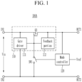
- FIG. 1 schematically illustrates an inrush current limiter.
- an inrush current limiter 100A includes input nodes IN1 and IN2 that are connected with a power source (not shown), output nodes OUT1 and OUT2 that are connected with a load (not shown), an inrush current limiting portion 110, a mode control switch SW1, and a mode controller 120.
- the inrush current limiting portion 110 is a circuit that is connected between the input nodes IN1 and IN2 and the output nodes OUT1 and OUT2 and performs an inrush current limitation function when power is connected.
- the inrush current limiting portion 110 includes a transistor Q1 connected between the input node IN1 and the output node OUT1, and may include a gate driver 111 connected between an input terminal and a control terminal, and a feedback portion 112 connected between an output terminal and a control terminal of the transistor Q1.
- the gate driver 111 controls the turn on of the transistor Q1 when an input voltage Vin of a first voltage level or higher is input, and may gradually increase a voltage between the control terminal and an input terminal of the transistor Q1 such that the transistor Q1 is fully turned on after a predetermined time period elapses after application of the input voltage Vin. On-resistance of the transistor Q1 is gradually decreased during the predetermined time period by the gate driver 111 after application of the input voltage Vin, and accordingly, a sudden current fluctuation due to the turn-on of the transistor Q1 does not occur, thereby limiting the inrush current.
- the feedback portion 112 is a negative feedback portion that is connected between the output terminal and the control terminal of the transistor Q1, and performs a function of suppressing the inrush current by stabilizing (or planarizing) a voltage between the control terminal and the input terminal of the transistor Q1. That is, the inrush current can be suppressed by suppressing the sudden fluctuation of the voltage between the control terminal and the input terminal of the transistor Q1.
- the mode control switch SW1 is connected between the control terminal of the transistor Q1 and the input node IN2 in the inrush current limiting portion 110, and performs a function of switching electrical connection between the input node IN2 and the control terminal of the transistor Q1.
- the mode control switch SW1 When the mode control switch SW1 is turned off, the transistor Q1 operates in an inrush current limitation mode during which the turning-on is controlled by the gate driver 111 in the inrush current limiting portion 110.
- the mode control switch SW1 is turned on, the control terminal of the transistor Q1 is electrically connected with the input node IN2, and the transistor Q1 operates in a mode (e.g., an EMC test mode) during which the turning-on is controlled according to the input voltage Vin regardless of operation of the gate driver 111.
- the control terminal of the transistor Q1 When the mode control switch SW1 is turned on, the control terminal of the transistor Q1 is directly connected to the input node IN2, and the input voltage Vin corresponds to a voltage between the input terminal and the control terminal of the transistor Q1. Accordingly, the transistor Q1 may be turned on when a voltage level of the input voltage Vin is equal to or higher than a threshold voltage level (hereinafter referred to as a second voltage level) of the transistor Q1.
- a threshold voltage level hereinafter referred to as a second voltage level
- the transistor Q1 When the mode control switch SW1 is turned off, that is, when the transistor Q1 operates in the inrush current limitation mode, the transistor Q1 is turned on by the gate driver 111 when the voltage level of the input voltage Vin is equal to or higher than a first voltage level.
- the gate driver 111 transmits a voltage divided from the input voltage Vin through a voltage divider circuit (not shown) to the control terminal of the transistor Q1, and this will be described later.
- the first voltage level that determines turning-on of the transistor Q1 in the inrush current limitation that the transistor Q1 is fully turned on after a predetermined time period elapses after application of the input voltage Vin.
- On-resistance of the transistor Q1 is gradually decreased during the predetermined time period by the gate driver 111 after application of the input voltage Vin, and accordingly, a sudden current fluctuation due to the turn-on of the transistor Q1 does not occur, thereby limiting the inrush current.
- the feedback portion 112 is a negative feedback portion that is connected between the output terminal and the control terminal of the transistor Q1, and performs a function of suppressing the inrush current by stabilizing (or planarizing) a voltage between the control terminal and the input terminal of the transistor Q1. That is, the inrush current can be suppressed by suppressing the sudden fluctuation of the voltage between the control terminal and the input terminal of the transistor Q1.
- the mode control switch SW1 is connected between the control terminal of the transistor Q1 and the input node IN2 in the inrush current limiting portion 110, and performs a function of switching electrical connection between the input node IN2 and the control terminal of the transistor Q1.
- the mode control switch SW1 When the mode control switch SW1 is turned off, the transistor Q1 operates in an inrush current limitation mode during which the turning-on is controlled by the gate driver 111 in the inrush current limiting portion 110.
- the mode control switch SW1 when the mode control switch SW1 is turned on, the control terminal of the transistor Q1 is electrically connected with the input node IN2, and the transistor Q1 may operate in a mode (e.g., an EMC test mode) during which the turning-on is controlled according to the input voltage Vin regardless of operation of the gate driver 111.
- a mode e.g., an EMC test mode
- the control terminal of the transistor Q1 When the mode control switch SW1 is turned on, the control terminal of the transistor Q1 is directly connected to the input node IN2, and the input voltage Vin corresponds to a voltage between the input terminal and the control terminal of the transistor Q1. Accordingly, the transistor Q1 may be turned on when a voltage level of the input voltage Vin is equal to or higher than a threshold voltage level (hereinafter referred to as a second voltage level) of the transistor Q1.
- a threshold voltage level hereinafter referred to as a second voltage level
- the transistor Q1 When the mode control switch SW1 is turned off, that is, when the transistor Q1 operates in the inrush current limitation mode, the transistor Q1 may be turned on by the gate driver 111 when the voltage level of the input voltage Vin is equal to or higher than a first voltage level.
- the gate driver 111 transmits a voltage divided from the input voltage Vin through a voltage divider circuit (not shown) to the control terminal of the transistor Q1, and this will be described later.
- the first voltage level that determines turning-on of the transistor Q1 in the inrush current limitation mode may be higher than the above-stated second voltage level.
- the mode controller 120 receives the input voltage Vin supplied from the power source, and controls turn-on/turn-off of the mode control switch SW1 according to a level of the received input voltage Vin. That is, the mode controller 120 compares the input voltage Vin or the voltage level of the voltage divided from the input voltage Vin with a predetermined reference voltage Vref or a reference voltage range, and controls switching of the mode control switch SW1 according to a comparison result.
- the mode controller 120 may turn on the mode control switch SW1 when the voltage level of the input voltage Vin or the voltage divided from the input voltage Vin is lower than the predetermined reference voltage Vref or lower than the lower limit of the predetermined reference voltage range in the turn-off state of the mode control switch SW1.
- the mode controller 120 may turn off the mode control switch SW1 when the voltage level of the input voltage Vin or the voltage divided from the input voltage Vin is higher than the predetermined reference voltage Vref or higher than the upper limit of the predetermined reference voltage range in the turn-on state of the mode control switch SW1.
- the upper limit and the lower limit of the reference voltage range may be set based on a reference voltage Vref input to the mode controller 120.
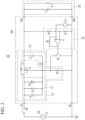
- FIG. 2 shows a system where the inrush current limiter according to the exemplary embodiment of the present invention is applied.
- a system 10A may include an inrush current limiter 100A that is connected between a power source 300 and a load 200.
- a system 10A may be, for example, a vehicle system.
- the power source 300 is electrically connected to the input nodes IN1 and IN2 of the inrush current limiter 100A and supplies an input voltage Vin to the inrush current limiter 100A.
- the power source 300 may be a high voltage battery back.
- the power source 300 may be an external power source for an EMC test.
- the power source 300 may supply an input voltage Vin from approximately 5 V to 58.5 V to the inrush current limiter 100A.
- the system 10A further includes a main switch SW2, and a connection with the inrush current limiter 100A may be controlled by the power source 300.
- the inrush current limiter 100A may include an inrush current limiting portion 110, a mode control switch SW1, and a mode controller 120.
- the inrush current limiting portion 110 may include a transistor Q1, a gate driver 111, and a feedback portion 112.
- the transistor Q1 may operate as a switch that is connected between an input node IN1 and an output node OUT1 to block or allow a current flow between the two nodes.
- the transistor Q1 may be, for example, a P-channel metal-oxide semiconductor field-effect transistor (P-channel MOSFET).
- P-channel MOSFET P-channel metal-oxide semiconductor field-effect transistor
- the exemplary embodiment of the present invention is not limited thereto, and the transistor Q1 may be an N-channel MOSFET.
- the input node IN2 of the inrush current limiter 100A may be connected to the positive output of the power source 300 and the input node IN1 may be connected to the negative output of the power source 300.
- the transistor Q1 is a P-channel MOSFET
- the gate driver 111 may include a first capacitor C1 and a first resistor R1 that are connected in parallel between a source and a gate of the transistor Q1, and a third resistor R3 that is connected between the gate of the transistor Q1 and the second input node IN2.
- a time constant that determines the time when the gate-source voltage Vgs of the transistor Q1 reaches the threshold voltage Vth of the transistor Q1 may be determined by capacitance of the first capacitor C1 and resistance values of the first resistor R1 and the third resistor R3.
- a voltage level of the input voltage Vin that turns on the transistor Q1 may be determined by the resistance values of the first resistor R1 and the third resistor R3.
- the gate driver 111 may further include a Zener diode ZD1 that includes a cathode connected to the source of the transistor Q1 and an anode connected to the gate of the transistor Q1.
- the Zener diode ZD1 may serve to limit the gate-source voltage Vgs of the transistor Q1 within its rated voltage.
- a voltage between lateral ends of the first capacitor C1 connected with the Zener diode ZD1 in parallel may be limited by the Zener diode ZD1.
- the feedback portion 112 may include a second capacitor C2 connected in series between a drain and the gate of the transistor Q1, and a second resistor R2. Such a feedback portion 112 provides a feedback path between the drain and the gate of the transistor Q1 to provide a function of suppressing an inrush current transmitted to a load-side capacitor C_L by stabilizing the gate-source voltage Vgs of the transistor Q1.
- the mode controller 120 may include a comparator U1 and voltage divider circuits R4 and R5.
- the voltage divider circuits R4 and R5 include a fourth resistor R4 and a fifth resistor R5 that are connected in series between the output node OUT1 and the input node IN2 (i.e., a ground), and divide a voltage, transmitted to the output node OUT1, through the transistor Q1 and transmit it as an input voltage of the comparator U1.
- the fourth resistor R4 is connected between the output node OUT1 and a first input terminal of the comparator U1
- the fifth resistor R5 may be connected between the first input terminal of the comparator U1 and the second input node IN2, that is, the ground.
- the comparator U1 may include a first input terminal (e.g., a negative input) that receives a voltage divided from the voltage divider circuits R4 and R5, a second input terminal (e.g., a positive input) to which the reference voltage Vref is input, and an output terminal outputting a control signal to the mode control switch SW1.
- a first input terminal e.g., a negative input
- a second input terminal e.g., a positive input
- the comparator U1 may output a signal (e.g., a high level signal) to turn on the mode control switch SW1 to the output terminal when the voltage received through the first input terminal is lower than the reference voltage Vref.
- the comparator U1 may output a signal (e.g., a high level signal) to turn off the mode control switch SW1 to the output terminal when the voltage input through the first input terminal is higher than the reference voltage Vref.
- the comparator U1 may be a hysteresis comparator.
- the hysteresis comparator U1 may operate by a hysteresis band (referred to as a reference voltage range in this specification) defined by an upper limit and a lower limit.
- the mode controller 120 may further include a sixth resistor R6 that is connected between the second input terminal and the output terminal of the comparator U1 and determines the hysteresis band of the comparator U1.
- the hysteresis band of the hysteresis comparator U1 is determined by a lower limit determined at a lower level and an upper limit determined at a higher level based on the reference voltage Vref input to the second input terminal of comparator U1, and the upper and lower limits may be determined by the sixth resistor R6.
- Such a hysteresis comparator U1 may output a signal (e.g., a high level signal) to turn on the mode control switch SW1 to the output terminal when a voltage input to the first input terminal is lower than the lower limit of the reference voltage range, and outputs a signal (e.g., a low level signal) to turn off the mode control switch SW1 to the output terminal when the voltage input to the first input terminal is higher than the upper limit of the reference voltage range.
- a signal e.g., a high level signal
- a signal e.g., a low level signal
- the above-described reference voltage Vref or the reference voltage range may be set so that the mode control switch SW1 can be turned on when the input voltage Vin has a lower voltage level than the first voltage level.
- the mode controller 120 that is, the comparator U1 of the mode controller 120
- the mode controller 120 is prevented from malfunctioning due to transmission of a part of the input voltage Vin to the output node OUT1 at the early connection stage of the power source 300, that is, while the inrush current limiting portion 110 performs an inrush current limitation operation, and in order to prevent power wastage due to unnecessary operation of the comparator U1 while performing the inrush current limiting operation, the comparator U1 may be controlled to be activated after a predetermined time after power from the power source 300 is applied.
- an operation voltage for operating the comparator U1 is applied after a predetermined delay after the power source 300 is connected such that the comparator U1 operates in a state in which the voltage transmitted to the load 200 through the output node OUT1 is stabilized. In such a state, the transistor Q1 is completely turned on (fully turned on) to operate in saturation, and an input voltage Vin may be applied to the output node OUT1.
- the mode controller 120 is connected to the output node OUT1 of the inrush current limiter 100A to monitor the input voltage Vin input from the power source 300 is described, but the exemplary embodiment of the present invention is not limited thereto.
- FIG. 3 schematically illustrates an inrush current limiter 100B according to another exemplary embodiment of the present invention
- FIG. 4 schematically illustrates a system 10B to which the inrush current limiter of FIG. 3 is applied.
- the inrush current limiter 100B and the system 10B according to another exemplary embodiment of the present invention are different from the inrush current limiter 100A and the system 10A according to the above-described exemplary embodiment of the present invention in that voltage divider circuits R4 and R5 are not connected to a first output node OUT1 but are connected to a first input node IN1. Therefore, hereinafter, in order to avoid unnecessary redundant description, descriptions of the remaining constituent elements that operate similarly to the inrush current limiters 100A and the system 10A described above will be omitted.
- a predetermined delay occurs until a voltage Vin supplied by a power source 300 is normally transmitted to an output node OUT1 due to operation of the inrush current limiting portion 110, and accordingly, a predetermined delay occurs until voltage divider circuits R4 and R5 transmit a voltage corresponding to the normal input voltage Vin to the comparator U1.
- the comparator U1 when the first input terminal of the comparator U1 is connected to the first input node IN1 through voltage divider circuits R4 and R5, the input voltage Vin is transmitted directly to the voltage divider circuits R4 and R5 when the power source 300 is connected, and accordingly, the comparator U1 also directly receives the voltage corresponding to the normal input voltage Vin.
- the comparator U1 may be activated after a predetermined time lapses after connection of the power source 300 so as to prevent occurrence of power waste due to unnecessary operation of the comparator U1 while the inrush current limiter 100B performs inrush current limitation operation.
- FIG. 5 schematically illustrates an operation timing diagram of the inrush current limiters 100A and 100B according to the exemplary embodiments of the present invention, and exemplarily illustrates a case that a low-voltage test voltage is applied for an EMC test after connection of the power source 300 to the systems 10A and 10B.
- the inrush current limiter 100A at the beginning of the connection of the power supply 300 operates in the inrush current limiting mode to suppress the inrush current transmitted to the load 200.
- the comparator U1 is activated for monitoring of the input voltage Vin, and the inrush current limiters 100A and 100B continuously monitor a voltage level of the input voltage Vin through the comparator U1 (Mode 1). In this case, the transistor Q1 is completely turned on and the comparator U1 operates in saturation.
- the mode controller 120 turns on the mode control switch SW1 when it detects that the input voltage Vin drops below the rated voltage of the system 10A for EMC tests while monitoring the input voltage Vin through the comparator U1 (Mode 2). That is, when the voltage input corresponding to the input voltage Vin is lower than a first threshold value VHL, an output signal V_out_comp for controlling the mode control switch SW1 to turn on is transmitted to a control terminal of the mode control switch SW1.
- the first threshold value VHL corresponds to the lower limit of the hysteresis band of the hysteresis comparator U1.
- the mode control switch SW1 when the voltage level of the input voltage Vin is higher than the threshold voltage level of the transistor Q1, the transistor Q1 may be completely turned on. Therefore, it is possible to operate the transistor Q1 even when a lower voltage than the rated voltage of systems 10A and 10B is input as in the case of the EMC test.
- the mode controller 120 continuously monitors the voltage level of the input voltage Vin through the comparator U1 even in the Mode 2 section, and turns off the mode control switch SW1 when it is detected that the input voltage Vin increases within the rated voltage range of the system 10A due to the termination of the EMC situation during the monitoring (Mode 4). That is, the comparator U1 controls an output signal V_out_comp to control the mode control switch SW1 to the turn off state when the voltage input corresponding to the input voltage Vin is higher than the second threshold value VHU.
- the second threshold value VHU corresponds to the upper limit of the hysteresis band of the hysteresis comparator U1.
- the mode control switch SW1 As the mode control switch SW1 is turned off, the inrush current limiters 100A and 100B return to the inrush current limit mode, and the turn on of the transistor Q1 is controlled by the gate driver 111 (Mode 5).
- the transistor Q1 is turned on even when the input voltage Vin is lower than the rated voltage of the systems 10A and 10B is input as in the EMC test process such that it is possible to prevent a situation where power is not supplied to the load 200 due to malfunction of the transistor Q1.
- An electronic or electrical device and/or any other related device or constituent element according to the exemplary embodiments of the present invention described herein can be implemented using any suitable hardware, firmware (e.g., application-specific integrated circuits), software, or a combination of software, firmware, and hardware.
- the elements of various configurations of the devices can be formed on a single integrated circuit (IC) chip or on separate IC chips.
- the elements of various configurations of the devices can be implemented as a flexible printed circuit film, a tape carrier package (TCP), or a printed circuit board (PCB), or may be implemented on a single substrate.
- the electrical connection or interconnection described in the present specification can be implemented by wire or conductive elements on, for example, a PCB or other type of circuit carrier.
- the conductive element may include metallization such as surface metallization and/or pins, and may include conductive polymers or ceramics.
- electrical energy may be transmitted through a wireless connection using, for example, electron radiation or light.
- the various configurations elements of the devices may be a process or a thread that runs on at least one processor and at least one computing device to perform the various functions described herein, executes computer program instructions, and interacts with other system constituent elements.
- the computer program instructions are stored in a memory that can be implemented in a computing device using standard memory devices, such as a random access memory (RAM).
- the computer program instructions may also be stored on other non-transitory computer readable media such as, for example, a CD-ROM, a flash drive, and the like.
Landscapes
- Engineering & Computer Science (AREA)
- Power Engineering (AREA)
- Physics & Mathematics (AREA)
- Electromagnetism (AREA)
- General Physics & Mathematics (AREA)
- Radar, Positioning & Navigation (AREA)
- Automation & Control Theory (AREA)
- Emergency Protection Circuit Devices (AREA)
- Direct Current Feeding And Distribution (AREA)
Claims (15)
- Einschaltstrombegrenzer (100A, 100B), umfassend:einen ersten Eingangsknoten, IN1, und einen zweiten Eingangsknoten, IN2, die eine Eingangsspannung Vin von einer Stromquelle (300) empfangen;einen ersten Ausgangsknoten, OUT1, und einen zweiten Ausgangsknoten, OUT2, die mit einer Last (200) verbunden sind;einen Einschaltstrombegrenzungsabschnitt (110), der einen Transistor, Q1, beinhaltet, der einen ersten Anschluss, der mit dem ersten Eingangsknoten, IN1, verbunden ist, einen zweiten Anschluss, der mit dem ersten Ausgangsknoten, OUT1, verbunden ist, und einen Steueranschluss aufweist, wobei das Einschalten des Transistors durch eine Spannung zwischen dem ersten Anschluss und dem Steueranschluss gesteuert wird;einen Schalter, SW1, der zwischen dem Steueranschluss des Transistors und dem zweiten Eingangsknoten, IN2, angeschlossen ist; undeinen Modus-Controller (120), der konfiguriert ist, um:den Schalter auszuschalten, wenn ein Spannungspegel der Eingangsspannung höher als ein erster Pegel, VHU, ist, undden Schalter einzuschalten, wenn der Spannungspegel der Eingangsspannung niedriger als ein zweiter Pegel, VHL, ist, wobei der zweite Pegel niedriger als der erste Pegel ist,wobei, wenn der Schalter ausgeschaltet ist, der Einschaltstrombegrenzungsabschnitt (110) dazu konfiguriert ist, den Transistor so zu steuern, dass er sich allmählich einschaltet, um einen Einschaltstrom zu begrenzen, undwenn der Schalter eingeschaltet ist und ein Spannungspegel der Eingangsspannung gleich oder höher als der zweite Pegel ist, die Eingangsspannung zwischen dem zweiten Eingangsknoten und dem Steueranschluss des Transistors angelegt wird, um den Transistor einzuschalten.
- Einschaltstrombegrenzer nach Anspruch 1, wobei der Einschaltstrombegrenzungsabschnitt (110) dazu angeordnet ist, das allmähliche Einschalten des Transistors zu steuern, indem er die Zeit steuert, bis der Transistor nach Anlegen der Eingangsspannung vollständig eingeschaltet ist.
- Einschaltstrombegrenzer nach Anspruch 1 oder 2, wobei der Transistor ein Metalloxid-Halbleiter-Feldeffekttransistor (MOSFET) ist,der erste Anschluss und der zweite Anschluss jeweils eine Quelle und ein Drain des Transistors sind undder Steueranschluss ein Gate des Transistors ist.
- Einschaltstrombegrenzer nach einem der vorhergehenden Ansprüche, wobei der der zweite Eingangsknoten mit einer elektrischen Masse verbunden ist.
- Einschaltstrombegrenzer nach einem der vorhergehenden Ansprüche, wobei der Einschaltstrombegrenzungsabschnitt (110) einen Gate-Treiber (111) umfasst, der dazu konfiguriert ist, eine Spannung zwischen dem ersten Anschluss und dem Steueranschluss allmählich zu erhöhen, wenn die Eingangsspannung eingegeben wird.
- Einschaltstrombegrenzer nach Anspruch 5, wobei der Gate-Treiber (111) umfasst: einen ersten Kondensator, C1;einen ersten Widerstand R1, der parallel zwischen dem ersten Anschluss und dem Steueranschluss angeschlossen ist; undeinen dritten Widerstand, R3, der zwischen dem Steueranschluss und dem zweiten Eingangsknoten angeschlossen ist.
- Einschaltstrombegrenzer nach Anspruch 6, wobei der Gate-Treiber (111) ferner eine Zenerdiode, ZD1, umfasst, die zwischen dem ersten Anschluss und dem Steueranschluss angeschlossen ist und dazu konfiguriert ist, eine Spannung zwischen dem ersten Anschluss und dem Steueranschluss zu begrenzen.
- Einschaltstrombegrenzer nach Anspruch 5, 6 oder 7, wobei der Einschaltstrombegrenzungsabschnitt (110) ferner einen Rückkopplungsabschnitt (112) umfasst, der zwischen dem zweiten Anschluss und dem Steueranschluss angeschlossen ist und dazu konfiguriert ist, eine Spannung zwischen dem ersten Anschluss und dem Steueranschluss zu stabilisieren.
- Einschaltstrombegrenzer nach Anspruch 8, wobei der Rückkopplungsabschnitt (112) umfasst:einen zweiten Kondensator, C2, der in Reihe zwischen dem ersten Anschluss und dem Steueranschluss geschaltet ist, undeinen zweiten Widerstand, R2.
- Einschaltstrombegrenzer nach einem der vorhergehenden Ansprüche, wobei der Modus-Controller (120) einen Komparator, U1, umfasst, wobei der Komparator umfasst:einen ersten Eingangsanschluss, an dem eine der Eingangsspannung entsprechende Vergleichsspannung eingegeben wird,einen zweiten Eingangsanschluss, an dem eine Referenzspannung, Vref, eingegeben wird, undeinen Ausgangsanschluss, der dazu konfiguriert ist, ein Ausgangssignal entsprechend einem Vergleichsergebnis von über den ersten und zweiten Eingangsanschluss eingegebenen Spannungen an einen Steueranschluss des Schalters auszugeben.
- Einschaltstrombegrenzer nach Anspruch 10, wobei der Modus-Controller (120) umfasst:
einen vierten Widerstand, R4, und einen fünften Widerstand, R5, die in Reihe geschaltet sind, und eine Spannungsteilerschaltung, die dazu konfiguriert ist, die aus der Eingangsspannung geteilte Vergleichsspannung an den ersten Eingangsanschluss auszugeben. - Einschaltstrombegrenzer nach Anspruch 11, wobei der Modus-Controller (120) ferner einen sechsten Widerstand, R6, umfasst, der zwischen dem zweiten Eingangsanschluss und dem Ausgangsanschluss des Komparators angeschlossen ist, und
der Komparator als Hysteresekomparator basierend auf einem Hystereseband mit einer Untergrenze, die niedriger als die Referenzspannung ist, und einer Obergrenze, die höher als die Referenzspannung ist, arbeitet und dazu konfiguriert ist, ein Ausgangssignal, das den Schalter einschaltet, an den Ausgangsanschluss auszugeben, wenn die Vergleichsspannung niedriger als die Untergrenze ist, und ein Ausgangssignal auszugeben, das den Schalter ausschaltet, wenn die Vergleichsspannung höher als die Obergrenze ist. - Einschaltstrombegrenzer nach Anspruch 11 oder 12, wobei der vierte Widerstand und der fünfte Widerstand zwischen dem ersten Ausgangsknoten und der Masse angeschlossen sind, und
der Komparator nach Ablauf einer vorgegebenen Zeitspanne nach Anlegen der Eingangsspannung aktiviert wird. - Einschaltstrombegrenzer nach Anspruch 11 oder 12, wobei der vierte Widerstand und der fünfte Widerstand zwischen dem ersten Eingangsknoten und der Masse angeschlossen sind.
- System, umfassend den Einschaltstrombegrenzer nach einem der vorhergehenden Ansprüche.
Applications Claiming Priority (1)
| Application Number | Priority Date | Filing Date | Title |
|---|---|---|---|
| KR1020200064398A KR102555498B1 (ko) | 2020-05-28 | 2020-05-28 | 돌입 전류 제한 장치 및 이를 포함하는 시스템 |
Publications (2)
| Publication Number | Publication Date |
|---|---|
| EP3916941A1 EP3916941A1 (de) | 2021-12-01 |
| EP3916941B1 true EP3916941B1 (de) | 2025-02-19 |
Family
ID=75625324
Family Applications (1)
| Application Number | Title | Priority Date | Filing Date |
|---|---|---|---|
| EP21169370.0A Active EP3916941B1 (de) | 2020-05-28 | 2021-04-20 | Einschaltstrombegrenzer und system damit |
Country Status (6)
| Country | Link |
|---|---|
| US (1) | US11539205B2 (de) |
| EP (1) | EP3916941B1 (de) |
| KR (1) | KR102555498B1 (de) |
| CN (1) | CN113746076B (de) |
| HU (1) | HUE070811T2 (de) |
| PL (1) | PL3916941T3 (de) |
Families Citing this family (7)
| Publication number | Priority date | Publication date | Assignee | Title |
|---|---|---|---|---|
| EP4372940A1 (de) * | 2022-11-18 | 2024-05-22 | Lilium eAircraft GmbH | Leistungsregler mit strombegrenzungsfunktion zum vorladen |
| KR20240082077A (ko) * | 2022-12-01 | 2024-06-10 | 삼성에스디아이 주식회사 | 돌입 전류 제한 장치 및 이를 포함하는 시스템 |
| US20240396325A1 (en) * | 2023-05-26 | 2024-11-28 | Texas Instruments Incorporated | Disable circuit for a current inrush limiter |
| TWI860817B (zh) * | 2023-08-18 | 2024-11-01 | 台達電子工業股份有限公司 | 可抑制湧浪電流的開關觸發器 |
| CN119496491A (zh) | 2023-08-18 | 2025-02-21 | 台达电子工业股份有限公司 | 可抑制涌浪电流的开关触发器 |
| KR20250060552A (ko) * | 2023-10-26 | 2025-05-07 | 삼성에스디아이 주식회사 | 돌입전류 저감 회로 |
| CN118380981B (zh) * | 2024-03-29 | 2025-02-11 | 北京华电众信技术股份有限公司 | 浪涌抑制电路和网络设备 |
Family Cites Families (15)
| Publication number | Priority date | Publication date | Assignee | Title |
|---|---|---|---|---|
| KR100453849B1 (ko) | 2002-04-27 | 2004-10-28 | 주식회사 동진아이엔피 | 스위칭전원공급장치의 보호장치 |
| US7099135B2 (en) * | 2002-11-05 | 2006-08-29 | Semiconductor Components Industries, L.L.C | Integrated inrush current limiter circuit and method |
| KR20110033485A (ko) * | 2009-09-25 | 2011-03-31 | (주)빅텍 | 돌입전류제한회로 |
| KR102077557B1 (ko) * | 2012-10-26 | 2020-02-14 | 온세미컨덕터코리아 주식회사 | 스위치 제어 회로 및 이를 포함하는 전력 공급 장치 |
| US8878593B2 (en) | 2012-10-26 | 2014-11-04 | Fairchild Korea Semiconductor Ltd. | Switch control circuit and power supply device including the same |
| KR101974024B1 (ko) * | 2012-11-26 | 2019-05-02 | 온세미컨덕터코리아 주식회사 | 저전압 차단 회로, 이를 포함하는 스위치 제어 회로 및 전력 공급 장치 |
| JP6381023B2 (ja) * | 2013-08-27 | 2018-08-29 | 矢崎総業株式会社 | 突入電流制限回路 |
| JP6369890B2 (ja) * | 2014-02-19 | 2018-08-08 | Necエンベデッドプロダクツ株式会社 | 電源用スイッチング回路、システム、及びプログラム |
| US9653912B2 (en) | 2014-12-16 | 2017-05-16 | Nxp B.V. | Inrush current limiter |
| US9627962B2 (en) * | 2015-03-09 | 2017-04-18 | Texas Instruments Incorporated | Fast blocking switch |
| CN205960636U (zh) * | 2016-07-25 | 2017-02-15 | 昆山龙腾光电有限公司 | 浪涌电流控制电路及供电装置 |
| JP6412092B2 (ja) | 2016-12-19 | 2018-10-24 | ファナック株式会社 | 突入電流防止回路、突入電流防止方法、及び突入電流防止用プログラム |
| JP7145726B2 (ja) * | 2018-10-19 | 2022-10-03 | 新電元工業株式会社 | 電源装置、及び突入電流防止回路 |
| CN109510448A (zh) * | 2018-11-09 | 2019-03-22 | 天津航空机电有限公司 | 一种航空变换器的浪涌抑制电路 |
| KR102163423B1 (ko) | 2018-11-29 | 2020-10-07 | 주식회사 아이티엠반도체 | 외장형 셀 블록으로 조립되는 배터리 모듈 및 그 설치방법 |
-
2020
- 2020-05-28 KR KR1020200064398A patent/KR102555498B1/ko active Active
-
2021
- 2021-04-12 CN CN202110389299.4A patent/CN113746076B/zh active Active
- 2021-04-13 US US17/229,436 patent/US11539205B2/en active Active
- 2021-04-20 PL PL21169370.0T patent/PL3916941T3/pl unknown
- 2021-04-20 HU HUE21169370A patent/HUE070811T2/hu unknown
- 2021-04-20 EP EP21169370.0A patent/EP3916941B1/de active Active
Also Published As
| Publication number | Publication date |
|---|---|
| KR20210147335A (ko) | 2021-12-07 |
| KR102555498B1 (ko) | 2023-07-12 |
| EP3916941A1 (de) | 2021-12-01 |
| CN113746076B (zh) | 2024-03-12 |
| PL3916941T3 (pl) | 2025-05-05 |
| US11539205B2 (en) | 2022-12-27 |
| HUE070811T2 (hu) | 2025-07-28 |
| US20210376596A1 (en) | 2021-12-02 |
| CN113746076A (zh) | 2021-12-03 |
Similar Documents
| Publication | Publication Date | Title |
|---|---|---|
| EP3916941A1 (de) | Einschaltstrombegrenzer und system damit | |
| US9214821B2 (en) | Charge/discharge control circuit and battery device | |
| US9627962B2 (en) | Fast blocking switch | |
| US10756720B2 (en) | Driver circuit for electronic switch | |
| US11271558B2 (en) | Smart electronic switch | |
| US9325168B2 (en) | Semiconductor device | |
| US10944392B2 (en) | Switch circuit and power supply system | |
| EP1671408A1 (de) | Leistungsschalterstruktur und -verfahren | |
| US7126801B2 (en) | Polarity protection implemented with a MOSFET | |
| US20130188287A1 (en) | Protection circuit, charge control circuit, and reverse current prevention method employing charge control circuit | |
| CN105914713A (zh) | 用于故障保护电路的系统和方法 | |
| US20190013725A1 (en) | Driving circuit for high-side transistor | |
| US20220001817A1 (en) | Vehicle power supply device | |
| US12592636B2 (en) | Power supply semiconductor device, including a delay circuit to protect power transistor | |
| US9541931B2 (en) | Regulator circuit and integrated circuit device forming the regulator circuit | |
| US10903644B2 (en) | Control device | |
| US10715043B2 (en) | Single inductor multiple output power converter with overload control | |
| US20230291396A1 (en) | Semiconductor device | |
| JP2020096444A (ja) | スイッチング回路 | |
| EP3471269B1 (de) | Schaltkreislauf zur verbindung und trennung einer elektrischen komponente zwischen einem hochspannungspotenzial und einem niederspannungspotenzial | |
| CN115407819A (zh) | 电压调节电路及其操作方法、以及芯片 | |
| JP7684366B2 (ja) | 突入電流制限装置およびこれを含むシステム | |
| US20250219398A1 (en) | Automotive-grade chip, protection circuit, and vehicle-mounted circuit | |
| US20250015706A1 (en) | Gate driving device and power converter | |
| US11081884B2 (en) | Semiconductor device |
Legal Events
| Date | Code | Title | Description |
|---|---|---|---|
| PUAI | Public reference made under article 153(3) epc to a published international application that has entered the european phase |
Free format text: ORIGINAL CODE: 0009012 |
|
| STAA | Information on the status of an ep patent application or granted ep patent |
Free format text: STATUS: REQUEST FOR EXAMINATION WAS MADE |
|
| 17P | Request for examination filed |
Effective date: 20210420 |
|
| AK | Designated contracting states |
Kind code of ref document: A1 Designated state(s): AL AT BE BG CH CY CZ DE DK EE ES FI FR GB GR HR HU IE IS IT LI LT LU LV MC MK MT NL NO PL PT RO RS SE SI SK SM TR |
|
| B565 | Issuance of search results under rule 164(2) epc |
Effective date: 20211015 |
|
| GRAP | Despatch of communication of intention to grant a patent |
Free format text: ORIGINAL CODE: EPIDOSNIGR1 |
|
| STAA | Information on the status of an ep patent application or granted ep patent |
Free format text: STATUS: GRANT OF PATENT IS INTENDED |
|
| RIC1 | Information provided on ipc code assigned before grant |
Ipc: H02H 9/00 20060101AFI20241015BHEP |
|
| INTG | Intention to grant announced |
Effective date: 20241025 |
|
| GRAS | Grant fee paid |
Free format text: ORIGINAL CODE: EPIDOSNIGR3 |
|
| GRAA | (expected) grant |
Free format text: ORIGINAL CODE: 0009210 |
|
| STAA | Information on the status of an ep patent application or granted ep patent |
Free format text: STATUS: THE PATENT HAS BEEN GRANTED |
|
| AK | Designated contracting states |
Kind code of ref document: B1 Designated state(s): AL AT BE BG CH CY CZ DE DK EE ES FI FR GB GR HR HU IE IS IT LI LT LU LV MC MK MT NL NO PL PT RO RS SE SI SK SM TR |
|
| REG | Reference to a national code |
Ref country code: GB Ref legal event code: FG4D |
|
| REG | Reference to a national code |
Ref country code: CH Ref legal event code: EP |
|
| REG | Reference to a national code |
Ref country code: IE Ref legal event code: FG4D |
|
| REG | Reference to a national code |
Ref country code: DE Ref legal event code: R096 Ref document number: 602021026241 Country of ref document: DE |
|
| REG | Reference to a national code |
Ref country code: SE Ref legal event code: TRGR |
|
| REG | Reference to a national code |
Ref country code: NL Ref legal event code: MP Effective date: 20250219 |
|
| PG25 | Lapsed in a contracting state [announced via postgrant information from national office to epo] |
Ref country code: RS Free format text: LAPSE BECAUSE OF FAILURE TO SUBMIT A TRANSLATION OF THE DESCRIPTION OR TO PAY THE FEE WITHIN THE PRESCRIBED TIME-LIMIT Effective date: 20250519 |
|
| PG25 | Lapsed in a contracting state [announced via postgrant information from national office to epo] |
Ref country code: FI Free format text: LAPSE BECAUSE OF FAILURE TO SUBMIT A TRANSLATION OF THE DESCRIPTION OR TO PAY THE FEE WITHIN THE PRESCRIBED TIME-LIMIT Effective date: 20250219 |
|
| PGFP | Annual fee paid to national office [announced via postgrant information from national office to epo] |
Ref country code: DE Payment date: 20250402 Year of fee payment: 5 |
|
| PG25 | Lapsed in a contracting state [announced via postgrant information from national office to epo] |
Ref country code: ES Free format text: LAPSE BECAUSE OF FAILURE TO SUBMIT A TRANSLATION OF THE DESCRIPTION OR TO PAY THE FEE WITHIN THE PRESCRIBED TIME-LIMIT Effective date: 20250219 |
|
| PGFP | Annual fee paid to national office [announced via postgrant information from national office to epo] |
Ref country code: GB Payment date: 20250401 Year of fee payment: 5 |
|
| REG | Reference to a national code |
Ref country code: LT Ref legal event code: MG9D |
|
| PG25 | Lapsed in a contracting state [announced via postgrant information from national office to epo] |
Ref country code: IS Free format text: LAPSE BECAUSE OF FAILURE TO SUBMIT A TRANSLATION OF THE DESCRIPTION OR TO PAY THE FEE WITHIN THE PRESCRIBED TIME-LIMIT Effective date: 20250619 Ref country code: NO Free format text: LAPSE BECAUSE OF FAILURE TO SUBMIT A TRANSLATION OF THE DESCRIPTION OR TO PAY THE FEE WITHIN THE PRESCRIBED TIME-LIMIT Effective date: 20250519 |
|
| PGFP | Annual fee paid to national office [announced via postgrant information from national office to epo] |
Ref country code: HU Payment date: 20250429 Year of fee payment: 5 |
|
| PG25 | Lapsed in a contracting state [announced via postgrant information from national office to epo] |
Ref country code: NL Free format text: LAPSE BECAUSE OF FAILURE TO SUBMIT A TRANSLATION OF THE DESCRIPTION OR TO PAY THE FEE WITHIN THE PRESCRIBED TIME-LIMIT Effective date: 20250219 |
|
| PG25 | Lapsed in a contracting state [announced via postgrant information from national office to epo] |
Ref country code: HR Free format text: LAPSE BECAUSE OF FAILURE TO SUBMIT A TRANSLATION OF THE DESCRIPTION OR TO PAY THE FEE WITHIN THE PRESCRIBED TIME-LIMIT Effective date: 20250219 |
|
| PG25 | Lapsed in a contracting state [announced via postgrant information from national office to epo] |
Ref country code: LV Free format text: LAPSE BECAUSE OF FAILURE TO SUBMIT A TRANSLATION OF THE DESCRIPTION OR TO PAY THE FEE WITHIN THE PRESCRIBED TIME-LIMIT Effective date: 20250219 Ref country code: PT Free format text: LAPSE BECAUSE OF FAILURE TO SUBMIT A TRANSLATION OF THE DESCRIPTION OR TO PAY THE FEE WITHIN THE PRESCRIBED TIME-LIMIT Effective date: 20250620 |
|
| PGFP | Annual fee paid to national office [announced via postgrant information from national office to epo] |
Ref country code: FR Payment date: 20250401 Year of fee payment: 5 |
|
| PG25 | Lapsed in a contracting state [announced via postgrant information from national office to epo] |
Ref country code: GR Free format text: LAPSE BECAUSE OF FAILURE TO SUBMIT A TRANSLATION OF THE DESCRIPTION OR TO PAY THE FEE WITHIN THE PRESCRIBED TIME-LIMIT Effective date: 20250520 Ref country code: BG Free format text: LAPSE BECAUSE OF FAILURE TO SUBMIT A TRANSLATION OF THE DESCRIPTION OR TO PAY THE FEE WITHIN THE PRESCRIBED TIME-LIMIT Effective date: 20250219 |
|
| REG | Reference to a national code |
Ref country code: HU Ref legal event code: AG4A Ref document number: E070811 Country of ref document: HU |
|
| REG | Reference to a national code |
Ref country code: AT Ref legal event code: MK05 Ref document number: 1769276 Country of ref document: AT Kind code of ref document: T Effective date: 20250219 |
|
| PG25 | Lapsed in a contracting state [announced via postgrant information from national office to epo] |
Ref country code: SM Free format text: LAPSE BECAUSE OF FAILURE TO SUBMIT A TRANSLATION OF THE DESCRIPTION OR TO PAY THE FEE WITHIN THE PRESCRIBED TIME-LIMIT Effective date: 20250219 |
|
| PG25 | Lapsed in a contracting state [announced via postgrant information from national office to epo] |
Ref country code: DK Free format text: LAPSE BECAUSE OF FAILURE TO SUBMIT A TRANSLATION OF THE DESCRIPTION OR TO PAY THE FEE WITHIN THE PRESCRIBED TIME-LIMIT Effective date: 20250219 |
|
| PG25 | Lapsed in a contracting state [announced via postgrant information from national office to epo] |
Ref country code: IT Free format text: LAPSE BECAUSE OF FAILURE TO SUBMIT A TRANSLATION OF THE DESCRIPTION OR TO PAY THE FEE WITHIN THE PRESCRIBED TIME-LIMIT Effective date: 20250219 |
|
| PG25 | Lapsed in a contracting state [announced via postgrant information from national office to epo] |
Ref country code: AT Free format text: LAPSE BECAUSE OF FAILURE TO SUBMIT A TRANSLATION OF THE DESCRIPTION OR TO PAY THE FEE WITHIN THE PRESCRIBED TIME-LIMIT Effective date: 20250219 |
|
| PG25 | Lapsed in a contracting state [announced via postgrant information from national office to epo] |
Ref country code: CZ Free format text: LAPSE BECAUSE OF FAILURE TO SUBMIT A TRANSLATION OF THE DESCRIPTION OR TO PAY THE FEE WITHIN THE PRESCRIBED TIME-LIMIT Effective date: 20250219 Ref country code: EE Free format text: LAPSE BECAUSE OF FAILURE TO SUBMIT A TRANSLATION OF THE DESCRIPTION OR TO PAY THE FEE WITHIN THE PRESCRIBED TIME-LIMIT Effective date: 20250219 |
|
| PG25 | Lapsed in a contracting state [announced via postgrant information from national office to epo] |
Ref country code: RO Free format text: LAPSE BECAUSE OF FAILURE TO SUBMIT A TRANSLATION OF THE DESCRIPTION OR TO PAY THE FEE WITHIN THE PRESCRIBED TIME-LIMIT Effective date: 20250219 |
|
| PG25 | Lapsed in a contracting state [announced via postgrant information from national office to epo] |
Ref country code: SK Free format text: LAPSE BECAUSE OF FAILURE TO SUBMIT A TRANSLATION OF THE DESCRIPTION OR TO PAY THE FEE WITHIN THE PRESCRIBED TIME-LIMIT Effective date: 20250219 |
|
| REG | Reference to a national code |
Ref country code: DE Ref legal event code: R097 Ref document number: 602021026241 Country of ref document: DE |
|
| REG | Reference to a national code |
Ref country code: CH Ref legal event code: H13 Free format text: ST27 STATUS EVENT CODE: U-0-0-H10-H13 (AS PROVIDED BY THE NATIONAL OFFICE) Effective date: 20251125 |
|
| PG25 | Lapsed in a contracting state [announced via postgrant information from national office to epo] |
Ref country code: LU Free format text: LAPSE BECAUSE OF NON-PAYMENT OF DUE FEES Effective date: 20250420 |
|
| PG25 | Lapsed in a contracting state [announced via postgrant information from national office to epo] |
Ref country code: MC Free format text: LAPSE BECAUSE OF FAILURE TO SUBMIT A TRANSLATION OF THE DESCRIPTION OR TO PAY THE FEE WITHIN THE PRESCRIBED TIME-LIMIT Effective date: 20250219 |
|
| PLBE | No opposition filed within time limit |
Free format text: ORIGINAL CODE: 0009261 |
|
| STAA | Information on the status of an ep patent application or granted ep patent |
Free format text: STATUS: NO OPPOSITION FILED WITHIN TIME LIMIT |
|
| REG | Reference to a national code |
Ref country code: BE Ref legal event code: MM Effective date: 20250430 |
|
| PG25 | Lapsed in a contracting state [announced via postgrant information from national office to epo] |
Ref country code: BE Free format text: LAPSE BECAUSE OF NON-PAYMENT OF DUE FEES Effective date: 20250430 |
|
| PG25 | Lapsed in a contracting state [announced via postgrant information from national office to epo] |
Ref country code: CH Free format text: LAPSE BECAUSE OF NON-PAYMENT OF DUE FEES Effective date: 20250430 |
|
| 26N | No opposition filed |
Effective date: 20251120 |
|
| PGFP | Annual fee paid to national office [announced via postgrant information from national office to epo] |
Ref country code: SE Payment date: 20260327 Year of fee payment: 6 |
|
| PG25 | Lapsed in a contracting state [announced via postgrant information from national office to epo] |
Ref country code: IE Free format text: LAPSE BECAUSE OF NON-PAYMENT OF DUE FEES Effective date: 20250420 |
|
| PGFP | Annual fee paid to national office [announced via postgrant information from national office to epo] |
Ref country code: PL Payment date: 20260327 Year of fee payment: 6 |