EP3917009A1 - Halbleiterbauelement mit passivem magneto-elektrischem wandler - Google Patents
Halbleiterbauelement mit passivem magneto-elektrischem wandler Download PDFInfo
- Publication number
- EP3917009A1 EP3917009A1 EP20472006.4A EP20472006A EP3917009A1 EP 3917009 A1 EP3917009 A1 EP 3917009A1 EP 20472006 A EP20472006 A EP 20472006A EP 3917009 A1 EP3917009 A1 EP 3917009A1
- Authority
- EP
- European Patent Office
- Prior art keywords
- semiconductor device
- layer
- diffusion region
- piezoelectric layer
- piezoelectric
- Prior art date
- Legal status (The legal status is an assumption and is not a legal conclusion. Google has not performed a legal analysis and makes no representation as to the accuracy of the status listed.)
- Granted
Links
Images

Classifications
-
- H—ELECTRICITY
- H03—ELECTRONIC CIRCUITRY
- H03K—PULSE TECHNIQUE
- H03K17/00—Electronic switching or gating, i.e. not by contact-making and –breaking
- H03K17/51—Electronic switching or gating, i.e. not by contact-making and –breaking characterised by the components used
- H03K17/80—Electronic switching or gating, i.e. not by contact-making and –breaking characterised by the components used using non-linear magnetic devices; using non-linear dielectric devices
-
- H—ELECTRICITY
- H01—ELECTRIC ELEMENTS
- H01H—ELECTRIC SWITCHES; RELAYS; SELECTORS; EMERGENCY PROTECTIVE DEVICES
- H01H36/00—Switches actuated by change of magnetic field or of electric field, e.g. by change of relative position of magnet and switch, by shielding
-
- H—ELECTRICITY
- H10—SEMICONDUCTOR DEVICES; ELECTRIC SOLID-STATE DEVICES NOT OTHERWISE PROVIDED FOR
- H10D—INORGANIC ELECTRIC SEMICONDUCTOR DEVICES
- H10D48/00—Individual devices not covered by groups H10D1/00 - H10D44/00
- H10D48/50—Devices controlled by mechanical forces, e.g. pressure
-
- G—PHYSICS
- G01—MEASURING; TESTING
- G01R—MEASURING ELECTRIC VARIABLES; MEASURING MAGNETIC VARIABLES
- G01R33/00—Arrangements or instruments for measuring magnetic variables
- G01R33/02—Measuring direction or magnitude of magnetic fields or magnetic flux
- G01R33/06—Measuring direction or magnitude of magnetic fields or magnetic flux using galvano-magnetic devices
- G01R33/09—Magnetoresistive devices
- G01R33/091—Constructional adaptation of the sensor to specific applications
-
- H—ELECTRICITY
- H03—ELECTRONIC CIRCUITRY
- H03K—PULSE TECHNIQUE
- H03K17/00—Electronic switching or gating, i.e. not by contact-making and –breaking
- H03K17/94—Electronic switching or gating, i.e. not by contact-making and –breaking characterised by the way in which the control signals are generated
- H03K17/945—Proximity switches
- H03K17/95—Proximity switches using a magnetic detector
- H03K17/9505—Constructional details
-
- H—ELECTRICITY
- H10—SEMICONDUCTOR DEVICES; ELECTRIC SOLID-STATE DEVICES NOT OTHERWISE PROVIDED FOR
- H10D—INORGANIC ELECTRIC SEMICONDUCTOR DEVICES
- H10D48/00—Individual devices not covered by groups H10D1/00 - H10D44/00
- H10D48/40—Devices controlled by magnetic fields
-
- H—ELECTRICITY
- H10—SEMICONDUCTOR DEVICES; ELECTRIC SOLID-STATE DEVICES NOT OTHERWISE PROVIDED FOR
- H10D—INORGANIC ELECTRIC SEMICONDUCTOR DEVICES
- H10D64/00—Electrodes of devices having potential barriers
- H10D64/60—Electrodes characterised by their materials
- H10D64/66—Electrodes having a conductor capacitively coupled to a semiconductor by an insulator, e.g. MIS electrodes
- H10D64/68—Electrodes having a conductor capacitively coupled to a semiconductor by an insulator, e.g. MIS electrodes characterised by the insulator, e.g. by the gate insulator
- H10D64/691—Electrodes having a conductor capacitively coupled to a semiconductor by an insulator, e.g. MIS electrodes characterised by the insulator, e.g. by the gate insulator comprising metallic compounds, e.g. metal oxides or metal silicates
-
- H—ELECTRICITY
- H10—SEMICONDUCTOR DEVICES; ELECTRIC SOLID-STATE DEVICES NOT OTHERWISE PROVIDED FOR
- H10D—INORGANIC ELECTRIC SEMICONDUCTOR DEVICES
- H10D64/00—Electrodes of devices having potential barriers
- H10D64/60—Electrodes characterised by their materials
- H10D64/66—Electrodes having a conductor capacitively coupled to a semiconductor by an insulator, e.g. MIS electrodes
- H10D64/68—Electrodes having a conductor capacitively coupled to a semiconductor by an insulator, e.g. MIS electrodes characterised by the insulator, e.g. by the gate insulator
- H10D64/693—Electrodes having a conductor capacitively coupled to a semiconductor by an insulator, e.g. MIS electrodes characterised by the insulator, e.g. by the gate insulator the insulator comprising nitrogen, e.g. nitrides, oxynitrides or nitrogen-doped materials
-
- H—ELECTRICITY
- H10—SEMICONDUCTOR DEVICES; ELECTRIC SOLID-STATE DEVICES NOT OTHERWISE PROVIDED FOR
- H10D—INORGANIC ELECTRIC SEMICONDUCTOR DEVICES
- H10D84/00—Integrated devices formed in or on semiconductor substrates that comprise only semiconducting layers, e.g. on Si wafers or on GaAs-on-Si wafers
Definitions
- the present invention is generally related to the field of semiconductor devices comprising a passive magneto-electric transducer structure and of passive magnetic switches.
- a reed switch is a well-known discrete electromechanical switch component that is operated by an applied magnetic field. It consists of a pair of contacts of ferrous metal reeds in a hermetically sealed glass envelope. The contacts may be normally open but closing when a magnetic field is present, or normally closed and opening when a magnetic field is applied.
- the switch may be actuated by a coil, making a reed relay, or by bringing a magnet near to the switch. Once the magnet is pulled away from the switch, the reed switch will go back to its original position.
- Reed switches are used for example as a proximity switch for a burglar alarm.
- the technology for making reed switches is very mature, but as such they cannot be integrated in semiconductor devices.
- a major advantage of reed switches is that they are passive devices, meaning that they do not require electrical energy for sensing the presence of a magnetic field.
- US6437558 is related to a system for detecting rotational speed of a rotor.
- the system comprises a passive magnetic field sensor with at least one multilayer material located adjacent to, but separate from, a rotatable rotor.
- the multilayer material contains a layer of a first thickness of a magnetostrictive material, connected across an interface to a layer of a second thickness of a piezoelectric material and configured so that, when the magnetostrictive material is subjected to a change in magnetic field from rotation of the rotor, a change in at least one dimension of the magnetostrictive material induces a strain in the piezoelectric material and produces a non-zero voltage signal in.
- EP3340323 B1 presents a semiconductor device comprising a passive magneto-electric transducer structure, a semiconductor switch connected thereto and a substrate.
- This substrate comprises an elastomer layer wherein the transducer structure is mounted.
- the transducer structure has a terminal electrically connected to the gate terminal of the switch.
- the invention relates to a semiconductor device comprising :
- the proposed solution indeed allows for obtaining a cost-efficient passive semiconductor device that can operate as a switch.
- said structure When the device is approached with a magnet, said structure is attracted towards the magnet, which, depending on the position of the magnet with respect to the semiconductor device, causes a tensile stress or a compression stress on the piezoelectric layer, which in turn leads to the formation of a charge above the dielectric layer, which in turn leads to the creation of a channel between the second and third diffusion region, thereby opening the switch.
- the structure has a surface with a larger area than the surface of the piezoelectric layer facing said structure. In embodiments the structure has a surface is in area at least twice said surface of the piezoelectric layer.
- the semiconductor device further comprises an additional structure arranged to perform mechanical stress on the piezoelectric layer in response to the magnetic field. Due to this additional structure a pulling force is created between the two structures which affects the piezoelectric layer to create a shear force.
- the additional structure is disposed on a support layer.
- support layer is a further piezoelectric layer.
- the semiconductor device further comprises a fourth diffusion region of the second type with embedded therein a fifth and a sixth diffusion region of the first type, said fifth and said sixth diffusion region more heavily doped than the fourth region, said fifth and sixth diffusion region each connected to a respective contact.
- the semiconductor device comprises a flexible layer whereon at least said structure is extended, said flexible layer having an opening to allow contact between said structure and the piezoelectric layer.
- the flexible layer also extends on said additional structure.
- the structure has a larger edge at an outside of the semiconductor device than at a side facing said additional structure.
- the semiconductor device comprises in a gap between the structure and the additional structure a further structure in a ferromagnetic material.
- the said further structure is thinner than said structure and said additional structure.
- the gap between said structures is comprised between 0.05 and 50 micron, most preferably between 0.05 and 5 micron.
- the semiconductor device is implemented as a field effect transistor.
- the structure and/or the additional structure is a magnetic concentrator.
- the piezoelectric layer is a polymer layer.
- the ratio of the thickness of the piezoelectric layer to the thickness of the structure is inversely proportional to the ratio of the stiffness of the piezoelectric layer to the stiffness of the structure.
- the piezoelectric layer has a surface of substantially the same area as the area of a chan nel created, when in use, between the second and third diffusion region by charge displacement in the piezoelectric layer.
- the present invention discloses in one aspect a semiconductor device comprising a passive magneto-electric transducer, meaning that the transducer does not require electrical energy for sensing the presence of a magnetic field.
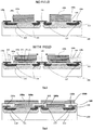
- Fig.1 illustrates an embodiment wherein the semiconductor device comprises a semiconductor substrate (50).
- the substrate may for example be a CMOS substrate.
- a diffusion region (110) lightly doped with a dopant of a first type, i.e. with either a p-type or n-type dopant.
- the lightly doped diffusion region (110) are provided the second and third regions (115) which are doped with the opposite type of dopant with a higher doping concentration than the lightly doped diffusion regions, i.e.
- the semiconductor device comprises two terminals that each form a contact with one of the regions (115). These contacts are made in an opening in a dielectric layer (120) provided on the substrate.
- the dielectric layer at least covers the surface of the substrate between the two regions (115), thereby including at least an edge of each of the two regions.
- the dielectric layer fulfils two functions. It serves as a gate and it provides insulation for the interconnect (contacts through this layer). Practically the dielectric layer between the source and drain may in some embodiments be as thin as a gate oxide (e.g.
- the semiconductor device further comprises a third terminal that acts as a control terminal, as will be detailed later in this description.
- the second and third diffusion region (115) are embedded in the first diffusion region (110), which itself forms the substrate.
- the semiconductor device is arranged to operate as a switch, so it switches between an open state and a closed state between terminal 130a and terminal 135.
- the magneto-electric transducer allows steering (controlling) the switch.
- the electrical resistive path between the two terminals changes, depending on the voltage applied to the control terminal.
- the electrical resistance is relatively low (ideally zero) and when the switch is in open state, the electrical resistance is relatively high (ideally infinitely high).
- the semiconductor device is a field effect transistor (FET).
- FET field effect transistor
- the two heavily doped regions (115), i.e. the second and the third region, then correspond to a source and a drain (or a drain and a source), respectively, and the contacts are a source contact and a drain contact.
- the second region may be the source and the third region the drain or vice versa.
- Any type of FET can be used in embodiments of the invention, for example any FET selected from the group consisting of JFET, MOSFET, MNOS, DGMOSFET, DEPFET, FREDFET, HIGFET, MODFET, TFET, IGBT, HEMT, MESFET, VeSFET, CNTFET, OFET, QFET.
- a magneto-electric transducer comprising a piezoelectric layer (140a) is placed on top of the dielectric layer (120).
- the piezeoelectric layer is disposed over, adjacent to or in contact with the dielectric layer.
- the semiconductor device has an electrode of the piezoelectric layer integrated with the control terminal of the semiconductor device (i.e. with the gate in case of an implementation as FET).
- a structure in a "soft" ferromagnetic material i.e. one that can be magnetized easily and substantially loses magnetization after the external magnetic field has been removed.
- this structure (150a) in ferromagnetic material is an integrated magnetic concentrator (IMC).
- the soft magnetic material is FeNi, i.e. a Nickel-Iron alloy.
- the structure may be a layer comprising material in for example FeGa, FeCo, FeTb, FeCoSiB or FeCoB.
- the IMC structure 150a When a magnet is approached to the soft-magnetic structure as illustrated in Fig.1 , i.e. from above the structure, the IMC structure 150a is attracted towards the magnet (a ferromagnetic structure is always attracted by a magnet regardless of whether it concerns a N or S pole) and generates a tensile stress (i.e. a stress tending to elongate the structure), in turn generating charges and opening the transistor. Similarly, if the magnet is approached from below the structure, a compression stress (i.e. a stress tending to shorten the structure) is generated.
- the behaviour is less than ideal and in such cases the voltage difference may appear like a spike, i.e. it can be a transient signal.
- the transient switch signal can be used to latch another signal.
- the charge displacement in the piezoelectric layer also has effect in the substrate : the conductivity under the dielectric layer (the gate oxide) changes and an inversion layer is created. One so obtains a channel between the second and third region (115) (i.e. between source and drain).
- the switch provides an electrical path with variable resistance, depending on the signal it receives from the magneto-electric transducer, more in particular from the piezoelectric layer.
- the area of the piezoelectric layer may be substantially equal to the area of the channel between the second and third region.
- the charge created by the piezoelectric layer directly modulates or inverts the conductivity under the dielectric layer without requiring an electrical connector or conductive plate between the piezoelectric layer and the gate. This also implies there is no need for an electrode at the top of the piezoelectric layer.
- the piezoelectric layer (140a) and the IMC structure 150a have the same area.
- the IMC structure 150a may bigger in area than the piezoelectric layer. This may be beneficial to increase the amount of stress created.
- the ratio of IMC structure area piezoelectric layer area may be in certain embodiments 2, 10 or even 100.
- the soft-magnetic structure 150a is extended on the flexible layer, which acts as a stress buffer.
- This flexible layer may for example be a polymer layer, e.g. polyimide or silicone.
- the piezoelectric layer is made in AIN, ZnO, AIScN or PZT.
- the switching functionality of the semiconductor device is realised by means of a FET.
- the semiconductor switch is assumed to be a FET. This however does in no way limit the scope of the present invention.
- the set-up of Fig.1 has been extended with an additional stack formed by an optional support layer 140b and a soft-magnetic structure 150b.
- the gap is less than one third or even one-tenth of the thickness of the soft-magnetic structures 150a and 150b to maximise the magnetic force between the two soft magnetic structures.
- the thickness of the soft magnetic structures is typically in the range of 1 to 100 ⁇ m, e.g. 20 ⁇ m.
- the support layer 140b may be disposed on, over, adjacent to or in contact with the dielectric layer.
- the support layer 140b may be a piezoelectric layer.
- the additional stack then constitutes a second magneto-electric transducer.
- the layer 140b may be produced in the same manufacturing step as piezoelectric layer 140a.
- the layer 140b is in another material than layer 140a, for example in SiO 2 .
- the layer 140b is then produced in a different manufacturing step.
- the structure 150b e.g. an integrated magnetic concentrator, similar to the structure 150a already discussed with respect to Fig.1 .
- an additional FET is positioned under the additional stack.
- the layer 140b in the additional stack is in this embodiment a piezoelectric layer, so that the stack of piezoelectric layer 140b and additional structure 150b forms a second magneto-electric transducer.
- a diffusion region (112) i.e. a fourth diffusion region, lightly doped with a dopant of the opposite type of the dopant in diffusion region (110).
- a fifth and a sixth region (117) (a source and a drain, or alternatively, a drain and a source) which are heavily doped with the opposite type of dopant, i.e.
- first region (112) is p-type doped
- regions (117) are n-type doped and vice versa.
- Two terminals are provided that form a source and a drain contact (135, 130b) (or drain and source contact), respectively.
- the piezoelectric layers (140a, 140b) preferably have an area substantially equal to the area of the channel created between the second and the third and the fifth and the sixth region, respectively.
- a terminal (135) may be shared between the two FETs.
- An opening is provided in the dielectric layer (gate oxide layer) for establishing a contact with each of the two regions (115,117). In other embodiments there is no common terminal and the two FETs have separate terminals with each a contact.
- one or more holes can be provided in the structure 150a and/or in additional structure 150b to reduce their stiffness.
- one surface of the piezoelectric layer is used as gate of the Field Effect Transistor (FET).
- FET Field Effect Transistor
- the gate terminal that acts as a control terminal in the semiconductor device is so integrated with the piezoelectric layer in embodiments according to the invention.
- the FET channel is made conductive by the charge on the piezoelectric layer created by a magnetic field applied to the soft-magnetic structures.
- the two magneto-electric transducers separated by a small gap are pulled together.
- the gap may be as narrow as one third or one tenth of the thickness of the soft magnetic structures 150.
- One FET channel is formed by a diffusion region 110 with a source and drain diffusion region 115 of the opposite type and contacted with the metal 130 and 135.
- the first diffusion region 110 is embedded in the substrate.
- the other FET channel is formed by the fourth diffusion region 112 (also embedded in the substrate in Fig.3 ) with a source and drain diffusion region 117 of the opposite type and contacted with the metal 130b and 135.
- a piezoelectric layer 140a, 140b such as AIN is placed on the gate oxide 120 above the channel areas.
- the soft magnetic structures 150a and 150b are placed on the piezoelectric layers 140a and 140b.
- the first diffusion region 110 itself is the substrate.
- the fourth diffusion region 112 is then embedded in the substrate, i.e. in the first diffusion region 110.
- the piezoelectric element may for example be dimensioned 100x100 ⁇ m or 20x20 ⁇ m.
- the piezoelectric element may have a rectangular shape with a length (L) and a width (W), where a ratio of the length and the width is a value in the range from 2 to 100 or from 2 to 40, for example in the range from 2 to 10, for example L/W equal to about 5.
- Both L and W have e.g. a value in the range of 5 to 200 ⁇ m.
- a smaller surface for example, 10x10 or 20x20 ⁇ m) offers the advantage that a smaller force is needed to generate the same stress on the piezo layer.
- the length of the gap can be smaller for a given thickness.
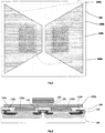
- Fig.4 illustrates a further embodiment of the device according to the invention.
- the soft-magnetic structures (150a, 150b) are made much larger than the piezoelectric structures by extending the soft-magnetic structures on a flexible layer (180).
- This flexible layer may for example be a polymer layer, e.g. polyimide or silicone. In other embodiments another elastomer can be used, e.g. PMDS.
- Embodiments as in Fig.4 are advantageous in that the force created in the entire soft-magnetic structure then is basically concentrated at the gap between the soft-magnetic structures (150a, 150b) on top of the flexible layer 180 and this gap can be made narrower than the gap between the piezoelectric structures (140a, 140b) by extending the soft-magnetic structures over the polymer layer (180).
- the force between the soft-magnetic structures (150a, 150b) is determined by the magnitude of the lateral magnetic field, the surface of the two facing walls of the soft-magnetic structures and the gap between the soft-magnetic structures.
- the flexible layer (180) By means of the flexible layer (180) one can make the surface of the soft-magnetic structures (150a, 150b) 2, 10 or even 100 times larger than the surface of the piezoelectric structures.
- the force between the larger soft-magnetic structures is then concentrated on the smaller surfaces of the piezoelectric structures (140a, 140b) as the flexible layer (180) does not counteract the displacement of the soft-magnetic structures.
- the stress generating the charge in the piezoelectric structures is then defined as the force between the (large) soft magnetic structures (150a, 150b) and only the (small) surface of the piezoelectric structures (140a, 140b). Therefore the structure presented in Fig.4 has clearly a much larger sensitivity than the structure presented in Fig.3 .
- Fig.5 shows another preferred embodiment.
- the soft magnetic structures 150a and 150b are so shaped that a much larger edge is defined at the outside of the structure than at the faces facing each other in the middle.
- the edges of the structure facing each other in the middle may have a length between 100 ⁇ m and 6 mm, for example 250 ⁇ m. This means that the magnetic field between the facing edges is amplified with a number that comes close to the ratio of the length of the edges at the outside divided by the length of the edges at the inside.
- This ratio of the length of the outer edges of the soft-magnetic structures and the length of their opposite edges may in embodiments of the invention range from 1 to 20 and consequently, also the amplification factor of the magnetic field may range from 1 to 20.
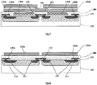
- Fig.6 and Fig.7 illustrate further embodiments of the semiconductor device.
- the devices as in Fig.6 and Fig.7 have undergone a further improvement by minimising the fringing field between two soft-magnetic structures (150a, 150b).
- the magnetic field between the soft-magnetic structures defines the force between the two structures and therefore the stress in the piezoelectric layers.
- the magnetic field in the gap decreases by forming fringing fields around the gap (not indicated in the figures). This effect can be minimised by making the gap much narrower than the height and width of the soft-magnetic structures (150a, 150b).
- Fringing fields are the peripheral magnetic fields outside of the magnet core.
- Fig.6 and Fig.7 show two possible realisations of a semiconductor device with minimum fringing fields.
- One way is to plate the outer structures (150a, 150b) with a gap larger than the thickness of these structures. These structures are then covered with a spacer layer without removing the seed layer for electroplating of the soft-magnetic structures.
- this spacer layer consists of or comprises an oxide or a metal that can be etched away selectively from the soft-magnetic structures and the seed layer used for plating the soft-magnetic structures.
- the sacrificial layer is only removed between the soft-magnetic structures 150 and a second electroplating step is carried out to grow an additional soft-magnetic structure 190 between the already formed soft-magnetic structures 150.
- the spacer layer can be removed by etching and also the seed layer for electroplating can be removed, outside the structures 150 and 190.
- the piezoelectric layer is realised by applying a doped polymer where an elastomer is filled with piezoelectric particles.
- Such piezoelectric particles consist of materials such as e.g. AIN, ZnO, AlScN or PZT, for example by using a printing technology.
- the soft-magnetic structures (150a, 150b) are disposed on top of the piezoelectric polymer layer (185). Note that in this embodiment the surface of the piezo electric layer cannot be smaller than the surface of the soft-magnetic structures.
- a computer program may be stored/distributed on a suitable medium, such as an optical storage medium or a solid-state medium supplied together with or as part of other hardware, but may also be distributed in other forms, such as via the Internet or other wired or wireless telecommunication systems. Any reference signs in the claims should not be construed as limiting the scope.
Landscapes
- Physics & Mathematics (AREA)
- Condensed Matter Physics & Semiconductors (AREA)
- General Physics & Mathematics (AREA)
- Nonlinear Science (AREA)
- Hall/Mr Elements (AREA)
- Pressure Sensors (AREA)
Priority Applications (3)
| Application Number | Priority Date | Filing Date | Title |
|---|---|---|---|
| EP20472006.4A EP3917009B1 (de) | 2020-05-29 | 2020-05-29 | Halbleiterbauelement mit passivem magneto-elektrischem wandler |
| US17/331,437 US12046685B2 (en) | 2020-05-29 | 2021-05-26 | Semiconductor device with passive magneto-electric transducer |
| CN202110592625.1A CN113871248A (zh) | 2020-05-29 | 2021-05-28 | 具有无源磁电换能器的半导体设备 |
Applications Claiming Priority (1)
| Application Number | Priority Date | Filing Date | Title |
|---|---|---|---|
| EP20472006.4A EP3917009B1 (de) | 2020-05-29 | 2020-05-29 | Halbleiterbauelement mit passivem magneto-elektrischem wandler |
Publications (2)
| Publication Number | Publication Date |
|---|---|
| EP3917009A1 true EP3917009A1 (de) | 2021-12-01 |
| EP3917009B1 EP3917009B1 (de) | 2024-12-25 |
Family
ID=71575339
Family Applications (1)
| Application Number | Title | Priority Date | Filing Date |
|---|---|---|---|
| EP20472006.4A Active EP3917009B1 (de) | 2020-05-29 | 2020-05-29 | Halbleiterbauelement mit passivem magneto-elektrischem wandler |
Country Status (3)
| Country | Link |
|---|---|
| US (1) | US12046685B2 (de) |
| EP (1) | EP3917009B1 (de) |
| CN (1) | CN113871248A (de) |
Citations (3)
| Publication number | Priority date | Publication date | Assignee | Title |
|---|---|---|---|---|
| EP0091739A1 (de) * | 1982-04-13 | 1983-10-19 | Minnesota Mining And Manufacturing Company | Integrierter, magnetostriktiver-piezoelektrischer MOS-Lese-Magnetkopf |
| US6437558B2 (en) | 1998-07-31 | 2002-08-20 | Spinix Corporation | Passive solid-state magnetic field sensors and applications therefor |
| EP3340323B1 (de) | 2016-12-22 | 2019-11-13 | Melexis Technologies NV | Halbleiterbauelement mit passiver magneto-elektrischer wandlerstruktur |
Family Cites Families (6)
| Publication number | Priority date | Publication date | Assignee | Title |
|---|---|---|---|---|
| US9082534B2 (en) * | 2009-09-15 | 2015-07-14 | Samsung Electronics Co., Ltd. | Magnetic element having perpendicular anisotropy with enhanced efficiency |
| US10379175B2 (en) * | 2010-07-20 | 2019-08-13 | King Abdullah University Of Science And Technology | Low-noise magnetic sensors |
| US9231191B2 (en) * | 2012-08-20 | 2016-01-05 | Industrial Technology Research Institute | Magnetic tunnel junction device and method of making same |
| JP6126565B2 (ja) * | 2014-09-19 | 2017-05-10 | 株式会社東芝 | 磁気抵抗素子及び磁気メモリ |
| JPWO2016158865A1 (ja) * | 2015-03-31 | 2018-01-25 | Tdk株式会社 | 磁気抵抗効果素子 |
| US10706903B2 (en) * | 2016-05-31 | 2020-07-07 | Sony Corporation | Nonvolatile memory cell, memory cell unit, and information writing method, and electronic apparatus |
-
2020
- 2020-05-29 EP EP20472006.4A patent/EP3917009B1/de active Active
-
2021
- 2021-05-26 US US17/331,437 patent/US12046685B2/en active Active
- 2021-05-28 CN CN202110592625.1A patent/CN113871248A/zh active Pending
Patent Citations (3)
| Publication number | Priority date | Publication date | Assignee | Title |
|---|---|---|---|---|
| EP0091739A1 (de) * | 1982-04-13 | 1983-10-19 | Minnesota Mining And Manufacturing Company | Integrierter, magnetostriktiver-piezoelektrischer MOS-Lese-Magnetkopf |
| US6437558B2 (en) | 1998-07-31 | 2002-08-20 | Spinix Corporation | Passive solid-state magnetic field sensors and applications therefor |
| EP3340323B1 (de) | 2016-12-22 | 2019-11-13 | Melexis Technologies NV | Halbleiterbauelement mit passiver magneto-elektrischer wandlerstruktur |
Also Published As
| Publication number | Publication date |
|---|---|
| EP3917009B1 (de) | 2024-12-25 |
| CN113871248A (zh) | 2021-12-31 |
| US20210376166A1 (en) | 2021-12-02 |
| US12046685B2 (en) | 2024-07-23 |
Similar Documents
| Publication | Publication Date | Title |
|---|---|---|
| US8320589B2 (en) | Electret condenser | |
| US4906586A (en) | Suspended gate field effect semiconductor pressure transducer device | |
| JP3521499B2 (ja) | 圧電/電歪膜型素子 | |
| US8247947B2 (en) | Coupling piezoelectric material generated stresses to devices formed in integrated circuits | |
| US20090302716A1 (en) | Piezoelectric device | |
| US5863024A (en) | Micro-Electromagnet including an integrated magnetic circuit and coil | |
| US20040056320A1 (en) | Microrelays and microrelay fabrication and operating methods | |
| US11527705B2 (en) | Semiconductor device comprising passive magnetoelectric transducer structure | |
| US3978508A (en) | Pressure sensitive field effect device | |
| US4678957A (en) | Piezoelectric ceramic switching devices and systems and methods of making the same | |
| KR102070851B1 (ko) | 나노로드 구조를 이용한 초음파 지문센서의 제조방법 | |
| EP3917009B1 (de) | Halbleiterbauelement mit passivem magneto-elektrischem wandler | |
| US8450912B2 (en) | Actuator element, method of driving actuator element, method of manufacturing actuator element, device inspection method and MEMS switch | |
| US7732991B2 (en) | Self-poling piezoelectric MEMs device | |
| US20240397828A1 (en) | Piezoelectric device having piezoelectric structure disposed between patterned conductive structures | |
| US20220359714A1 (en) | Electronic device provided with a stack of two high electron mobility transistors arranged in a bridge half-arm | |
| CN116314335A (zh) | 一种沟槽型mosfet器件的制造方法 | |
| JP2718767B2 (ja) | 半導体デバイス及びその応力制御方法 | |
| USRE33568E (en) | Piezoelectric ceramic switching devices and systems and methods of making the same | |
| EP2690418A1 (de) | Drucksensor mit flexibler Membran mit aktiven Schaltungskomponenten darauf | |
| USRE33618E (en) | Method for initially polarizing and centering a piezoelectric ceramic switching device | |
| KR102449792B1 (ko) | 유연 자기 센서 제조방법 및 이에 의해 제조된 유연 자기 센서 | |
| KR100668614B1 (ko) | 압전 구동 방식 저항형 rf mems 스위치 및 그 제조방법 | |
| CN1838837B (zh) | 固体电容式结构微型传声器 | |
| JPS6188417A (ja) | 無接点スイッチの製造方法 |
Legal Events
| Date | Code | Title | Description |
|---|---|---|---|
| PUAI | Public reference made under article 153(3) epc to a published international application that has entered the european phase |
Free format text: ORIGINAL CODE: 0009012 |
|
| STAA | Information on the status of an ep patent application or granted ep patent |
Free format text: STATUS: THE APPLICATION HAS BEEN PUBLISHED |
|
| AK | Designated contracting states |
Kind code of ref document: A1 Designated state(s): AL AT BE BG CH CY CZ DE DK EE ES FI FR GB GR HR HU IE IS IT LI LT LU LV MC MK MT NL NO PL PT RO RS SE SI SK SM TR |
|
| B565 | Issuance of search results under rule 164(2) epc |
Effective date: 20201109 |
|
| STAA | Information on the status of an ep patent application or granted ep patent |
Free format text: STATUS: REQUEST FOR EXAMINATION WAS MADE |
|
| 17P | Request for examination filed |
Effective date: 20220520 |
|
| RBV | Designated contracting states (corrected) |
Designated state(s): AL AT BE BG CH CY CZ DE DK EE ES FI FR GB GR HR HU IE IS IT LI LT LU LV MC MK MT NL NO PL PT RO RS SE SI SK SM TR |
|
| STAA | Information on the status of an ep patent application or granted ep patent |
Free format text: STATUS: EXAMINATION IS IN PROGRESS |
|
| 17Q | First examination report despatched |
Effective date: 20230209 |
|
| RIC1 | Information provided on ipc code assigned before grant |
Ipc: H03K 17/95 20060101ALI20240701BHEP Ipc: H03K 17/80 20060101AFI20240701BHEP |
|
| RAP3 | Party data changed (applicant data changed or rights of an application transferred) |
Owner name: MELEXIS BULGARIA LTD |
|
| GRAP | Despatch of communication of intention to grant a patent |
Free format text: ORIGINAL CODE: EPIDOSNIGR1 |
|
| STAA | Information on the status of an ep patent application or granted ep patent |
Free format text: STATUS: GRANT OF PATENT IS INTENDED |
|
| INTG | Intention to grant announced |
Effective date: 20240829 |
|
| GRAS | Grant fee paid |
Free format text: ORIGINAL CODE: EPIDOSNIGR3 |
|
| GRAA | (expected) grant |
Free format text: ORIGINAL CODE: 0009210 |
|
| STAA | Information on the status of an ep patent application or granted ep patent |
Free format text: STATUS: THE PATENT HAS BEEN GRANTED |
|
| AK | Designated contracting states |
Kind code of ref document: B1 Designated state(s): AL AT BE BG CH CY CZ DE DK EE ES FI FR GB GR HR HU IE IS IT LI LT LU LV MC MK MT NL NO PL PT RO RS SE SI SK SM TR |
|
| REG | Reference to a national code |
Ref country code: GB Ref legal event code: FG4D |
|
| REG | Reference to a national code |
Ref country code: CH Ref legal event code: EP |
|
| REG | Reference to a national code |
Ref country code: DE Ref legal event code: R096 Ref document number: 602020043623 Country of ref document: DE |
|
| REG | Reference to a national code |
Ref country code: IE Ref legal event code: FG4D |
|
| REG | Reference to a national code |
Ref country code: LT Ref legal event code: MG9D |
|
| PG25 | Lapsed in a contracting state [announced via postgrant information from national office to epo] |
Ref country code: HR Free format text: LAPSE BECAUSE OF FAILURE TO SUBMIT A TRANSLATION OF THE DESCRIPTION OR TO PAY THE FEE WITHIN THE PRESCRIBED TIME-LIMIT Effective date: 20241225 |
|
| PG25 | Lapsed in a contracting state [announced via postgrant information from national office to epo] |
Ref country code: FI Free format text: LAPSE BECAUSE OF FAILURE TO SUBMIT A TRANSLATION OF THE DESCRIPTION OR TO PAY THE FEE WITHIN THE PRESCRIBED TIME-LIMIT Effective date: 20241225 |
|
| PG25 | Lapsed in a contracting state [announced via postgrant information from national office to epo] |
Ref country code: BG Free format text: LAPSE BECAUSE OF FAILURE TO SUBMIT A TRANSLATION OF THE DESCRIPTION OR TO PAY THE FEE WITHIN THE PRESCRIBED TIME-LIMIT Effective date: 20241225 |
|
| PG25 | Lapsed in a contracting state [announced via postgrant information from national office to epo] |
Ref country code: NO Free format text: LAPSE BECAUSE OF FAILURE TO SUBMIT A TRANSLATION OF THE DESCRIPTION OR TO PAY THE FEE WITHIN THE PRESCRIBED TIME-LIMIT Effective date: 20250325 |
|
| PG25 | Lapsed in a contracting state [announced via postgrant information from national office to epo] |
Ref country code: LV Free format text: LAPSE BECAUSE OF FAILURE TO SUBMIT A TRANSLATION OF THE DESCRIPTION OR TO PAY THE FEE WITHIN THE PRESCRIBED TIME-LIMIT Effective date: 20241225 Ref country code: GR Free format text: LAPSE BECAUSE OF FAILURE TO SUBMIT A TRANSLATION OF THE DESCRIPTION OR TO PAY THE FEE WITHIN THE PRESCRIBED TIME-LIMIT Effective date: 20250326 |
|
| PG25 | Lapsed in a contracting state [announced via postgrant information from national office to epo] |
Ref country code: RS Free format text: LAPSE BECAUSE OF FAILURE TO SUBMIT A TRANSLATION OF THE DESCRIPTION OR TO PAY THE FEE WITHIN THE PRESCRIBED TIME-LIMIT Effective date: 20250325 |
|
| REG | Reference to a national code |
Ref country code: NL Ref legal event code: MP Effective date: 20241225 |
|
| P01 | Opt-out of the competence of the unified patent court (upc) registered |
Free format text: CASE NUMBER: APP_15933/2025 Effective date: 20250401 |
|
| PG25 | Lapsed in a contracting state [announced via postgrant information from national office to epo] |
Ref country code: NL Free format text: LAPSE BECAUSE OF FAILURE TO SUBMIT A TRANSLATION OF THE DESCRIPTION OR TO PAY THE FEE WITHIN THE PRESCRIBED TIME-LIMIT Effective date: 20241225 |
|
| REG | Reference to a national code |
Ref country code: AT Ref legal event code: MK05 Ref document number: 1755039 Country of ref document: AT Kind code of ref document: T Effective date: 20241225 |
|
| PG25 | Lapsed in a contracting state [announced via postgrant information from national office to epo] |
Ref country code: SM Free format text: LAPSE BECAUSE OF FAILURE TO SUBMIT A TRANSLATION OF THE DESCRIPTION OR TO PAY THE FEE WITHIN THE PRESCRIBED TIME-LIMIT Effective date: 20241225 |
|
| PG25 | Lapsed in a contracting state [announced via postgrant information from national office to epo] |
Ref country code: PL Free format text: LAPSE BECAUSE OF FAILURE TO SUBMIT A TRANSLATION OF THE DESCRIPTION OR TO PAY THE FEE WITHIN THE PRESCRIBED TIME-LIMIT Effective date: 20241225 |
|
| PGFP | Annual fee paid to national office [announced via postgrant information from national office to epo] |
Ref country code: DE Payment date: 20250423 Year of fee payment: 6 |
|
| PG25 | Lapsed in a contracting state [announced via postgrant information from national office to epo] |
Ref country code: ES Free format text: LAPSE BECAUSE OF FAILURE TO SUBMIT A TRANSLATION OF THE DESCRIPTION OR TO PAY THE FEE WITHIN THE PRESCRIBED TIME-LIMIT Effective date: 20241225 |
|
| PG25 | Lapsed in a contracting state [announced via postgrant information from national office to epo] |
Ref country code: IS Free format text: LAPSE BECAUSE OF FAILURE TO SUBMIT A TRANSLATION OF THE DESCRIPTION OR TO PAY THE FEE WITHIN THE PRESCRIBED TIME-LIMIT Effective date: 20250425 |
|
| PG25 | Lapsed in a contracting state [announced via postgrant information from national office to epo] |
Ref country code: PT Free format text: LAPSE BECAUSE OF FAILURE TO SUBMIT A TRANSLATION OF THE DESCRIPTION OR TO PAY THE FEE WITHIN THE PRESCRIBED TIME-LIMIT Effective date: 20250428 |
|
| PG25 | Lapsed in a contracting state [announced via postgrant information from national office to epo] |
Ref country code: EE Free format text: LAPSE BECAUSE OF FAILURE TO SUBMIT A TRANSLATION OF THE DESCRIPTION OR TO PAY THE FEE WITHIN THE PRESCRIBED TIME-LIMIT Effective date: 20241225 |
|
| PGFP | Annual fee paid to national office [announced via postgrant information from national office to epo] |
Ref country code: FR Payment date: 20250423 Year of fee payment: 6 |
|
| PG25 | Lapsed in a contracting state [announced via postgrant information from national office to epo] |
Ref country code: RO Free format text: LAPSE BECAUSE OF FAILURE TO SUBMIT A TRANSLATION OF THE DESCRIPTION OR TO PAY THE FEE WITHIN THE PRESCRIBED TIME-LIMIT Effective date: 20241225 Ref country code: AT Free format text: LAPSE BECAUSE OF FAILURE TO SUBMIT A TRANSLATION OF THE DESCRIPTION OR TO PAY THE FEE WITHIN THE PRESCRIBED TIME-LIMIT Effective date: 20241225 |
|
| PG25 | Lapsed in a contracting state [announced via postgrant information from national office to epo] |
Ref country code: SK Free format text: LAPSE BECAUSE OF FAILURE TO SUBMIT A TRANSLATION OF THE DESCRIPTION OR TO PAY THE FEE WITHIN THE PRESCRIBED TIME-LIMIT Effective date: 20241225 |
|
| PG25 | Lapsed in a contracting state [announced via postgrant information from national office to epo] |
Ref country code: CZ Free format text: LAPSE BECAUSE OF FAILURE TO SUBMIT A TRANSLATION OF THE DESCRIPTION OR TO PAY THE FEE WITHIN THE PRESCRIBED TIME-LIMIT Effective date: 20241225 |
|
| PG25 | Lapsed in a contracting state [announced via postgrant information from national office to epo] |
Ref country code: IT Free format text: LAPSE BECAUSE OF FAILURE TO SUBMIT A TRANSLATION OF THE DESCRIPTION OR TO PAY THE FEE WITHIN THE PRESCRIBED TIME-LIMIT Effective date: 20241225 |
|
| PG25 | Lapsed in a contracting state [announced via postgrant information from national office to epo] |
Ref country code: SE Free format text: LAPSE BECAUSE OF FAILURE TO SUBMIT A TRANSLATION OF THE DESCRIPTION OR TO PAY THE FEE WITHIN THE PRESCRIBED TIME-LIMIT Effective date: 20241225 |
|
| REG | Reference to a national code |
Ref country code: DE Ref legal event code: R097 Ref document number: 602020043623 Country of ref document: DE |
|
| PG25 | Lapsed in a contracting state [announced via postgrant information from national office to epo] |
Ref country code: DK Free format text: LAPSE BECAUSE OF FAILURE TO SUBMIT A TRANSLATION OF THE DESCRIPTION OR TO PAY THE FEE WITHIN THE PRESCRIBED TIME-LIMIT Effective date: 20241225 |
|
| PLBE | No opposition filed within time limit |
Free format text: ORIGINAL CODE: 0009261 |
|
| STAA | Information on the status of an ep patent application or granted ep patent |
Free format text: STATUS: NO OPPOSITION FILED WITHIN TIME LIMIT |
|
| REG | Reference to a national code |
Ref country code: CH Ref legal event code: L10 Free format text: ST27 STATUS EVENT CODE: U-0-0-L10-L00 (AS PROVIDED BY THE NATIONAL OFFICE) Effective date: 20251105 |
|
| 26N | No opposition filed |
Effective date: 20250926 |
|
| REG | Reference to a national code |
Ref country code: CH Ref legal event code: H13 Free format text: ST27 STATUS EVENT CODE: U-0-0-H10-H13 (AS PROVIDED BY THE NATIONAL OFFICE) Effective date: 20251223 |
|
| PG25 | Lapsed in a contracting state [announced via postgrant information from national office to epo] |
Ref country code: LU Free format text: LAPSE BECAUSE OF NON-PAYMENT OF DUE FEES Effective date: 20250529 |
|
| PG25 | Lapsed in a contracting state [announced via postgrant information from national office to epo] |
Ref country code: CH Free format text: LAPSE BECAUSE OF NON-PAYMENT OF DUE FEES Effective date: 20250531 |
|
| GBPC | Gb: european patent ceased through non-payment of renewal fee |
Effective date: 20250529 |
|
| REG | Reference to a national code |
Ref country code: BE Ref legal event code: MM Effective date: 20250531 |
|
| PG25 | Lapsed in a contracting state [announced via postgrant information from national office to epo] |
Ref country code: MC Free format text: LAPSE BECAUSE OF FAILURE TO SUBMIT A TRANSLATION OF THE DESCRIPTION OR TO PAY THE FEE WITHIN THE PRESCRIBED TIME-LIMIT Effective date: 20241225 |