EP3919948B1 - Film guide lumineux et son procédé de production, et dispositif guide lumineux - Google Patents
Film guide lumineux et son procédé de production, et dispositif guide lumineux Download PDFInfo
- Publication number
- EP3919948B1 EP3919948B1 EP21759001.7A EP21759001A EP3919948B1 EP 3919948 B1 EP3919948 B1 EP 3919948B1 EP 21759001 A EP21759001 A EP 21759001A EP 3919948 B1 EP3919948 B1 EP 3919948B1
- Authority
- EP
- European Patent Office
- Prior art keywords
- light guide
- light
- guide film
- ultrastructure
- reflecting surface
- Prior art date
- Legal status (The legal status is an assumption and is not a legal conclusion. Google has not performed a legal analysis and makes no representation as to the accuracy of the status listed.)
- Active
Links
Images


Classifications
-
- G—PHYSICS
- G02—OPTICS
- G02B—OPTICAL ELEMENTS, SYSTEMS OR APPARATUS
- G02B6/00—Light guides; Structural details of arrangements comprising light guides and other optical elements, e.g. couplings
- G02B6/0001—Light guides; Structural details of arrangements comprising light guides and other optical elements, e.g. couplings specially adapted for lighting devices or systems
- G02B6/0011—Light guides; Structural details of arrangements comprising light guides and other optical elements, e.g. couplings specially adapted for lighting devices or systems the light guides being planar or of plate-like form
- G02B6/0033—Means for improving the coupling-out of light from the light guide
- G02B6/005—Means for improving the coupling-out of light from the light guide provided by one optical element, or plurality thereof, placed on the light output side of the light guide
- G02B6/0055—Reflecting element, sheet or layer
-
- G—PHYSICS
- G02—OPTICS
- G02B—OPTICAL ELEMENTS, SYSTEMS OR APPARATUS
- G02B6/00—Light guides; Structural details of arrangements comprising light guides and other optical elements, e.g. couplings
- G02B6/0001—Light guides; Structural details of arrangements comprising light guides and other optical elements, e.g. couplings specially adapted for lighting devices or systems
- G02B6/0011—Light guides; Structural details of arrangements comprising light guides and other optical elements, e.g. couplings specially adapted for lighting devices or systems the light guides being planar or of plate-like form
- G02B6/0033—Means for improving the coupling-out of light from the light guide
- G02B6/005—Means for improving the coupling-out of light from the light guide provided by one optical element, or plurality thereof, placed on the light output side of the light guide
- G02B6/0053—Prismatic sheet or layer; Brightness enhancement element, sheet or layer
-
- G—PHYSICS
- G02—OPTICS
- G02B—OPTICAL ELEMENTS, SYSTEMS OR APPARATUS
- G02B6/00—Light guides; Structural details of arrangements comprising light guides and other optical elements, e.g. couplings
- G02B6/0001—Light guides; Structural details of arrangements comprising light guides and other optical elements, e.g. couplings specially adapted for lighting devices or systems
- G02B6/0011—Light guides; Structural details of arrangements comprising light guides and other optical elements, e.g. couplings specially adapted for lighting devices or systems the light guides being planar or of plate-like form
- G02B6/0013—Means for improving the coupling-in of light from the light source into the light guide
- G02B6/0015—Means for improving the coupling-in of light from the light source into the light guide provided on the surface of the light guide or in the bulk of it
-
- G—PHYSICS
- G02—OPTICS
- G02B—OPTICAL ELEMENTS, SYSTEMS OR APPARATUS
- G02B6/00—Light guides; Structural details of arrangements comprising light guides and other optical elements, e.g. couplings
- G02B6/0001—Light guides; Structural details of arrangements comprising light guides and other optical elements, e.g. couplings specially adapted for lighting devices or systems
- G02B6/0011—Light guides; Structural details of arrangements comprising light guides and other optical elements, e.g. couplings specially adapted for lighting devices or systems the light guides being planar or of plate-like form
- G02B6/0013—Means for improving the coupling-in of light from the light source into the light guide
- G02B6/0023—Means for improving the coupling-in of light from the light source into the light guide provided by one optical element, or plurality thereof, placed between the light guide and the light source, or around the light source
- G02B6/0028—Light guide, e.g. taper
-
- G—PHYSICS
- G02—OPTICS
- G02B—OPTICAL ELEMENTS, SYSTEMS OR APPARATUS
- G02B6/00—Light guides; Structural details of arrangements comprising light guides and other optical elements, e.g. couplings
- G02B6/0001—Light guides; Structural details of arrangements comprising light guides and other optical elements, e.g. couplings specially adapted for lighting devices or systems
- G02B6/0011—Light guides; Structural details of arrangements comprising light guides and other optical elements, e.g. couplings specially adapted for lighting devices or systems the light guides being planar or of plate-like form
- G02B6/0033—Means for improving the coupling-out of light from the light guide
- G02B6/0035—Means for improving the coupling-out of light from the light guide provided on the surface of the light guide or in the bulk of it
- G02B6/004—Scattering dots or dot-like elements, e.g. microbeads, scattering particles, nanoparticles
- G02B6/0041—Scattering dots or dot-like elements, e.g. microbeads, scattering particles, nanoparticles provided in the bulk of the light guide
-
- G—PHYSICS
- G02—OPTICS
- G02B—OPTICAL ELEMENTS, SYSTEMS OR APPARATUS
- G02B6/00—Light guides; Structural details of arrangements comprising light guides and other optical elements, e.g. couplings
- G02B6/0001—Light guides; Structural details of arrangements comprising light guides and other optical elements, e.g. couplings specially adapted for lighting devices or systems
- G02B6/0011—Light guides; Structural details of arrangements comprising light guides and other optical elements, e.g. couplings specially adapted for lighting devices or systems the light guides being planar or of plate-like form
- G02B6/0033—Means for improving the coupling-out of light from the light guide
- G02B6/0058—Means for improving the coupling-out of light from the light guide varying in density, size, shape or depth along the light guide
- G02B6/0061—Means for improving the coupling-out of light from the light guide varying in density, size, shape or depth along the light guide to provide homogeneous light output intensity
-
- G—PHYSICS
- G02—OPTICS
- G02B—OPTICAL ELEMENTS, SYSTEMS OR APPARATUS
- G02B6/00—Light guides; Structural details of arrangements comprising light guides and other optical elements, e.g. couplings
- G02B6/0001—Light guides; Structural details of arrangements comprising light guides and other optical elements, e.g. couplings specially adapted for lighting devices or systems
- G02B6/0011—Light guides; Structural details of arrangements comprising light guides and other optical elements, e.g. couplings specially adapted for lighting devices or systems the light guides being planar or of plate-like form
- G02B6/0065—Manufacturing aspects; Material aspects
Definitions
- the application relates to the field of light guide materials, and more particularly, to a light guide film, a production method thereof and a light guide device.
- a light guide structure is commonly found in a light guide plate, and the light guide plate is a high-tech product for converting a linear light source into a surface light source.
- Light guide spots are printed on the bottom surface of an optical-grade acrylic/PC plate by using an engraving printing technology.
- the light emitted from the light source is absorbed by the optical-grade acrylic plate and is continuously and totally reflected inside the plate, when the light irradiates each light guide spot, the reflected light can be diffused at various angles, and then emitted from the front surface of the light guide plate after breaking the reflection condition.
- the light guide plate can emit light uniformly through various light guide spots with different densities and sizes.
- the light guide plate is high in manufacturing cost and precise in optical structure, and the whole light guide plate needs to be wasted once being damaged.
- the light guide plate is replaced by combining a light guide film with a transparent substrate, such as Chinese patent application with the publication number of CN102565923A , a composite light guide plate is disclosed, which has a transparent substrate and a transparent film, and a plurality of light guide spots are printed on the transparent film and attached to the back surface of the transparent substrate.
- the above solution is to print the light guide spots on the transparent film firstly, and then combine the transparent film printed with the light guide spots with the transparent substrate, to form the composite light guide plate.
- the light guide spots are printed on the transparent thin film, it is easier to implement than direct printing on the transparent substrate, which reduces manufacturing difficulty, and even if bad scrapping occurs, only the part of the transparent film needs to be scrapped while the part of the transparent substrate is intact, so that the cost can be reduced.
- WO2019224705A1 discloses a controlled light distribution element, which comprises a lightguide medium configured for light propagation, a first functional layer configured as an optical filter layer and disposed on an at least one surface of the lightguide medium,and a second functional layer comprising an at least one optically functional pattern, wherein the first functional layer and the second functional layer are rendered with an at least one optical function related to incident light and,in particular, to light incident at an angle equal and/or below the critical angle.
- the patent No. WO2019087118A1 discloses a light distribution structure and a related element 100, such as a light guide.
- the structure 10 is preferably an optically functional layer comprising an at least one feature pattern 11, 11A established in a light-transmitting carrier by a plurality of three-dimensional optical features variable in terms of at least one of the cross-sectional profile, dimensions, periodicity. orientation and disposition thereof within the feature pattern.
- the optical features are embodied as internal optical cavities 12 capable to establish the total internal reflection (TIR) function at a horizontal surface and at an essentially vertical surface thereof.
- TIR total internal reflection
- the patent No. WO2019182098A1 discloses an optical device which realizes uniform light distribution and sufficient display quality with a simple structure.
- the optical device has light guide layer, a first optical functional layer, a light control structure.
- the patent No. US2013315534A1 discloses a system and method for using bubble structures to control the extraction of light from a waveguide top surface.
- the method determines a maximum angle (a) of light propagation through a waveguide medium relative to a first horizontal direction parallel to a waveguide top surface.
- a plurality of bubble structures is provided having a refractive index less than the waveguide medium.
- the bubble structures have a base, and sides formed at an acute angle upwards with respect to the base.
- the bubble structure bases are separated by gap (W), have a height (H), and have a top separated from a waveguide top surface by a space (h).
- the method varies the gap (W), the height (H), and the space (h). In response, the intensity oflight extraction at even the maximum angle ( ⁇ ) of light propagation, can be controlled from the waveguide top surface.
- the patent No. US2011244187A1 is directed to techniques to manufacture internal cavity optical patterns and to apparatuses manufactured using the manufacturing techniques.
- Internal cavity optical patterns include small cavities (e.g., microcavities, nanocavities, etc.) spread across a surface of a thin transparent material.
- the thin material may then be laminated to a second material to join the surface having the cavities with the second material and thereby enclose the cavities within the resulting combination.
- the internal cavities may be filled with air or another medium (e.g., a fluid, gas, or solid), which enable the cavity to redirect light in accordance with design requirements.
- the cavities may remain free of debris that may reduce an effectiveness of the optics.
- additional layers of material may be laminated together to create additional layers of the internal cavity optics.
- the above-mentioned solution has certain drawbacks, because the transparent film and the transparent substrate are separately arranged, the firmness of the bonding between the transparent film and the transparent substrate should be considered when the transparent film and the transparent substrate are bonded.
- the light guide points are arranged on the transparent film, when the surface with the light guide points on the transparent film is in contact with the transparent substrate, not the surface-to-surface bonding but the point-to-surface bonding is adopted between the two.
- the transparent film and the transparent substrate are not made of the same material, and the point-to-surface bonding is easy to separate, which is not beneficial for long-term use.
- this application provides a light guide film, a production method thereof and a light guide device, which can improve the bonding area and intensity between the light guide film and the substrate, and better protect the ultrastructure without affecting the light guiding effect.
- a light guide film is provided, an upper surface of the light guide film is a light exit surface and a lower surface is a light incident surface; the lower surface of the light guide film is smooth, and used for being connected with a transparent substrate; a plurality of hollow ultrastructures are disposed in the light guide film, each hollow ultrastructure includes a conduction reflecting surface close to the lower surface of the light guide film, a top surface close to the upper surface of the light guide film, and a light exit reflecting surface connecting the conduction reflecting surface and the top surface, and a gap between every two adjacent ultrastructures is a light exit gap, a distance between the bottom line of the conduction reflecting surface and the light incident surface is 0.001-1 mm, the conduction reflecting surface is a curved surface, and an included angle between a tangent plane at any point on the curved surface and the light incident surface is less than 10°, and the light guide film is made of a soft material.
- the lower surface of the light guide film is smoothly arranged, so that when the lower surface of the light guide film is fixed with the substrate, the whole surface can be bonded, the contact area is maximized, the fixing effect can also be optimized, and the light guide film and the substrate are not easy to separate.
- a hollow ultrastructure is arranged inside the light guide film, so that light can be guided, light directly emitted to the hollow ultrastructure from the substrate can be totally reflected, light emitted to the light exit gap from the substrate can be finally emitted from the light exit surface, thereby achieving the light guide function.
- the ultrastructure of the light guide is arranged inside the light guide film, so that the ultrastructure for light guide is not easy to damage and has stronger stretch-resistant capability.
- the hollow ultrastructure is sealed by the conduction reflecting surface, the top surface and the light exit reflecting surface, and the interior of the hollow ultrastructure is air, or other material having a large difference from the refractive index of the film material, and light emitted to the conduction reflecting surface may be totally reflected, and the optical path extends within the substrate. Light emitted to the light exit gap is emitted onto the light exit reflecting surface, and then reflected and emitted from the light exit surface.
- a plurality of hollow ultrastructures are arranged inside the light guide film to play a role of guiding light, and the included angle between the light reflecting surface and the light exit reflecting surface, and the size of the light exit gap are controlled, so as to control the light path, and light rays are gradually distributed on the light exit surface of the whole light guide film.
- the conduction reflecting surface is a curved surface, the included angle between a tangent plane at any point on the curved surface and the light incident surface is less than 10°.
- the conduction reflecting surface when the conduction reflecting surface is a flat surface, the conduction reflecting surface can be parallel to the light incident surface, and the reflection path of light is regular.
- the conduction reflecting surface is a curved surface, the light path is irregular, and different light guiding effects and differentiated visual effects are generated.
- the light exit reflecting surface is an inclined surface or a curved surface; when the light exit reflecting surface is an inclined surface, the included angle between the light exit reflecting surface and the light incident surface is 45° to 85°; when the light exit reflecting surface is a curved surface, the included angle between a tangent plane at any point on the curved surface and the light incident surface is 45° to 85°.
- the angle of the cambered surface is arranged in advance, such that the light rays are vertically emitted to the light exit surface as much as possible, after the light lays are reflected by the cambered surface, so that light rays emitted from the light exit surfaces reaches the maximum light intensity, substantially remains uniform, and the light rays are emitted more uniformly.
- the distance between the bottom line of the conduction reflecting surface and the light incident surface is 0.001-1 mm, and the bottom lines of all the conduction reflecting surfaces are equidistant or non-equidistant from the light incident surface.
- the ultrastructure is arranged on the surface of the light guide film, and light rays pass through the substrate and then are directly emitted to the ultrastructure, so that the light utilization efficiency is very high.
- the ultrastructure in order to achieve a better bonding effect between the light guide film and the substrate, the ultrastructure is arranged inside the light guide film, therefore, the ultrastructure and the substrate are spaced apart by a thin layer of light guide film, which has a certain influence on the light path, and light needs to pass through the thin layer of film before reaching the ultrastructure. Therefore, the thinner the thin layer of film, the smaller the effect of the thin film on light refraction, the smaller the change of the light path; generally, when the thickness of the thin film is less than 1mm, and the light path change is negligible.
- the light exit gap between every two adjacent ultrastructures are equidistant or non-equidistant.
- the light exit gap between ultrastructures can be equidistant or non-equidistant, if equidistant, the light emission is relatively uniform; and if non-equidistant, the light guiding efficiency of each light exit gap can be changed, so that the light finally emitted from the light guide film is significantly changed, and the visual effect is better.
- This application further provides a process for producing a light guide film, which includes the following steps of:
- the polymer material can be selected from transparent silicone, or other transparent thermosetting or thermoplastic polymer materials, and an integrally formed light guide film, the process is simpler, and the hollow ultrastructure is arranged inside the light guide film, and is not easily damaged by itself and has a stronger stretch-resistant capability while guiding light.
- the ultrastructure is disposed inside the light guide film, it is difficult to form at a time through a single mold.
- the mold is divided into two parts, and the light guide film is divided into two parts, which are respectively formed.
- the two materials are attached by utilizing the characteristics of the silica gel material, so that curing forming is realized.
- the upper die or the lower die is provided with a micro-structure matching with the ultrastructure.
- the precision of the ultrastructure is too high. If the upper die and the lower die each has a part of the ultrastructure, the precise bonding cannot be ensured when the last two parts of the finished product are bonded, the ultrastructure is easily displaced, which affects the light guiding effect. Therefore, the micro-structure is individually disposed in the upper die or the lower die, so that one of the molded finished products has an ultrastructure and can be bonded to another finished product, thereby ensuring accuracy of the ultrastructure.
- This application further provides a process for producing a light guide film, which includes the following steps of:
- the light guide film can be formed at a time through a single mold, the process is simpler, the molding effect is better, and the light guide film is not easily deformed.
- This application further provides a process for producing a light guide film, which includes the following steps of:
- the light guide film can be formed at a time through a single mold, the process is simpler, the molding effect is better, and the light guide film is not easily deformed.
- This application further provides a light guide device, which includes the light guide film described above, and further includes a transparent substrate, wherein a lower surface of the light guide film is fixed to the transparent substrate.
- the lower surface of the light guide film is a smoothly transitioned flat surface, so that when the light guide film is fixed to the substrate, the whole surface can be attached, the contact area reaches the maximum, the fixing effect can be optimized, and the light guide film and the substrate are not easy to separate.
- a protective layer is arranged on the upper surface of the light guide film.
- the light guide film is made of a soft material and is easily stained with dirt such as dust, the light emitting effect can be improved by additionally arranging the protective layer, and cleaning is also convenient.
- the protection layer is preferably made of PET, and the PET is good in light transmittance, good in bonding effect with a silica gel light guide film, stable in physical performance and not prone to abrasion and deformation.
- the present application has the following beneficial effects: the lower surface of the light guide film is smoothly arranged, so that when the lower surface of the light guide film is fixed with the substrate, the whole surface can be bonded, the contact area is maximized, the fixing effect can also be optimized, and the light guide film and the substrate are not easy to separate. Meanwhile, the ultrastructure is arranged inside the light guide film, so that light can be guided, the ultrastructure is not easy to damage and has stronger stretch-resistant capability.
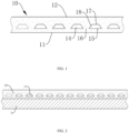
- substrate 4. protective layer; 10. light guide film; 11. light incident surface; 12. light exit surface; 14. Ultrastructure; 15. conduction reflecting surface; 16. light exit gap; 17. top surface; 18. light exit reflecting surface; 21. upper die; 22. lower die; 23. micro-structure.
- a light guide film 10 is provided, an upper surface of the light guide film 10 is a light exit surface 12, and a lower surface of the light guide film 10 is a light incident surface 11.
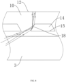
- the lower surface of the light guide film 10 is smooth and is used for being fixedly connected with the substrate 3 (see FIG. 2 ).
- a plurality of hollow ultrastructures 14 are disposed in the light guide film 10, and a side of the hollow ultrastructures 14 close to the lower surface of the light guide film 10 is a conduction reflecting surface 15, and a gap between every two adjacent ultrastructures 14 is a light exit gap 16.
- the lower surface of the light guide film 10 is arranged to be smooth, so that when the light guide film 10 is fixed to the substrate 3, the whole surface can be attached, the contact area reaches the maximum, the fixing effect can be optimized, and the light guide film 10 and the substrate 3 are not easy to separate.
- the hollow ultrastructure 14 includes a conduction reflecting surface 15 close to the lower surface of the light guide film 10, a top surface 17 close to the upper surface of the light guide film 10, and a light exit reflecting surface 18 connecting the conduction reflecting surface 15 and the top surface 17.
- the hollow ultrastructure 14 is disposed inside the light guide film 10, so that light can be guided, light directly emitted from the substrate 3 to the hollow ultrastructure 14 can be totally reflected, light emitted from the substrate 3 to the light exit gap 16 can be finally emitted from the light exit surface 12, thereby achieving the light guide function. Furthermore, the light guide ultrastructure is disposed inside the light guide film 10, so that the light guide film 10 is not easy to damage and stronger in stretch-resistant capability.
- the hollow ultrastructure 14 is sealed by the conduction reflecting surface 15, the top surface 17 and the light exit reflecting surface 18, and the interior of the hollow ultrastructure 14 is air, or other material having a large difference from the refractive index of the film material, and light emitted to the conduction reflecting surface 15 may be totally reflected, and the optical path extends within the substrate 3. Light emitted to the light exit gap 16 is emitted onto the light exit reflecting surface 18, and then reflected and emitted from the light exit surface 12.
- a plurality of hollow ultrastructures 14 are arranged inside the light guide film 10 to play a role of guiding light, and the included angle between the light reflecting surface 15 and the light exit reflecting surface 18, and the size of the light exit gap 16 are controlled, so as to control the light path, and light rays are gradually distributed on the light exit surface 12 of the whole light guide film 10.
- the top surface 17 since the top surface 17 has no light guiding effect, the top surface 17 can be designed in any shape, such as a flat surface, a cambered surface, a dot, or the like, as shown in FIG. 3 .
- the light exit gaps 16 between the ultrastructures 14 may be equidistant or non-equidistant, as shown in FIG. 4 .
- the conduction reflecting surface 15 may be a flat surface, in embodiments not part of the claimed invention, or a curved surface, in embodiments according to the claimed invention, and an included angle between a tangent plane at any point on the curved surface and the light incident surface is less than 10°.
- the light distribution can be achieved according to different designs, so that there is a sense of hierarchy when light is emitted.
- the first one is that the light rays are emitted to the junction between the substrate 3 and the light guide film 10, refracted into the light guide film 10, and then emitted to the light exit gap 16 between light guide structures in the light guide film 10, and the light continues to pass through the light exit gap 16 and is emitted to the light exit reflecting surface 18. Since the other side of the light exit reflecting surface 18 is a hollow ultrastructure 14, the refractive index of the air is low, the light rays are totally reflected on the light exit reflecting surface 18 and are emitted from the light exit surface 12.
- the second one is that the light rays are emitted to the junction between the substrate 3 and the light guide film 10, refracted into the light guide film 10, and then emitted to the lower surface of the hollow ultrastructure 14 in the light guide film 10, that is, the conduction reflecting surface 15. Since the other side of the conduction reflecting surface 15 is a hollow ultrastructure 14, the refractive index of the air is low, the light rays are totally reflected on the conduction reflecting surface 15 and are emitted back to the substrate 3. The light rays continue to be totally reflected on one side of the substrate 3 away from the light guide film 10, and are emitted to the light guide film 10 again.
- the light rays are emitted to the conduction reflecting surface 15 of the hollow ultrastructure 14 after passing through the light guide film 10, the light rays continue to be totally reflected repeatedly; if the light rays are emitted to the light exit gap 16 between the light guide structures after passing through the light guide film 10, the light rays are emitted from the light exit surface 12, as with the first case described above.
- the third one is that the light rays are emitted to the one side of the substrate 3 away from the light guide film 10, and then are emitted to the light guide film 10 after being totally reflected, if the light rays are emitted to the light exit gap 16 between the light guide structures after passing through the light guide film 10, then the light rays are as with the first case described above; if the light rays are emitted to the conduction reflecting surface 15 of the hollow ultrastructure 14 after passing through the light guide film 10, then the light rays are as with the second case described above.
- the distance between the conduction reflecting surface 15 and the light incident surface 11 is 0.001-1 mm.
- the ultrastructure 14 is arranged on the surface of the light guide film 10, and light rays pass through the substrate 3 and then are directly emitted to the ultrastructure 14, so that the light utilization efficiency is very high.
- the ultrastructure 14 in order to achieve a better bonding effect between the light guide film 10 and the substrate 3, the ultrastructure 14 is arranged inside the light guide film 10, therefore, the ultrastructure 14 and the substrate 3 are spaced apart by a thin layer of light guide film 10, which has a certain influence on the light path, and light needs to pass through the thin layer of film before reaching the ultrastructure 14. Therefore, the thinner the thin layer of film, the smaller the effect of the thin film on light refraction, the smaller the change of the light path; generally, when the thickness of the thin film is less than 1mm, and the light path change is negligible.
- the distance between the conduction reflecting surface 15 and the light incident surface 11 is 0.001-1 mm, preferably 0.6 mm.
- the distance has certain influence on the light path, and after the light passes through the substrate 3, the light needs to be emitted to the conduction reflecting surface 15 or the light exit gap 16 only after passing through the small distance. Therefore, the shorter the distance, the smaller the effect of the thin film on light refraction, the smaller the change of the light path; when the thickness of the thin film is less than 1mm, and the light path change is negligible.
- the height of the conduction reflecting surface 15 to the light incident surface 11 of each ultrastructure 14 may be uniform or non-uniform, if uniform, the light emission is relatively uniform; and if non-uniform, as shown in FIG. 5 , different light guiding effects and differentiated visual effects are generated.
- the conduction reflecting surface 15 may be a flat surface or a curved surface.
- the conduction reflecting surface 15 can be parallel to the light incident surface, and the reflection path of light is regular.
- the conduction reflecting surface 15 is a curved surface, the included angle between a tangent plane at any point on the curved surface and the light incident surface is less than 10°, the light path is irregular, the light distribution can be achieved according to different designs, and different light guiding effects and differentiated visual effects are generated.
- Embodiment 1 differs from Embodiment 1 in that, in this embodiment, the light exit reflecting surface 18 is a cambered surface.
- FIG. 8 it is shown a light emitting path when the light exit reflecting surface 18 is an inclined surface in Embodiment 1.
- the light rays are irradiated on the inclined surface, the light rays are reflected and then irradiated on the light exit surface 12, and since the angles of the light irradiated on the inclined surface are different, the angles of the light irradiated on the light exit surface 12 after being reflected are also different, and the intensity of the light emitted is different.
- the light exit reflecting surface 18 is arranged as a cambered surface.
- the included angle between a tangent plane at any point on the curved surface and the light incident surface is 45° to 85°.
- the angle of the cambered surface is designed such that the light rays are vertically emitted to the light exit surface 12 as much as possible, after the light lays are reflected by the cambered surface, so that light rays emitted from the light exit surfaces 12 reaches the maximum light intensity, substantially remains uniform, and the light rays are emitted more uniformly.
- the height of the light exit reflecting surface 18 is 0.5-3 times of the light exit gap 16, so that the number of the light exit gaps 16 that light passes through can be controlled, thus the light reflected out of the light guide film from the light exit reflecting surface 18 can be controlled, and the light emitting efficiency of the light guide film can be controlled.
- This embodiment provides a production process of a hollow ultrastructure light guide film, which is used for producing the light guide film of Embodiment 1, and the production process includes the following steps of:
- An integrally formed light guide film the process is simpler, and the hollow ultrastructure is arranged inside the light guide film, and is not easily damaged by itself and has a stronger stretch-resistant capability while guiding light.
- Embodiment 3 differs from Embodiment 3 in that, the light guide film is formed by hollow extrusion molding.
- the mold includes a micro-structure core mold, the raw materials are molded in the mold, and then stretched after leaving a die orifice, to obtain the light guide film with a hollow ultrastructure.
- the light guide film can be formed at a time through a single mold, the process is simpler, the molding effect is better, and the light guide film is not easily deformed.
- this embodiment differs from Embodiment 1 in that, in this embodiment, the mold includes an upper die 21 and a lower die 22, and after the raw materials are respectively injected into the upper die 21 and the lower die 22, the semi-finished raw materials are removed from the mold after the raw materials are semi-formed, and the semi-finished raw materials are bonded to each other before being fully cured.
- the ultrastructure is disposed inside the light guide film, it is difficult to form at a time through a single mold.
- the mold is divided into two parts, and the light guide film is divided into two parts, which are respectively formed.
- the two materials are attached by utilizing the characteristics of the silica gel material, so that curing forming is realized.
- the upper die 21 or the lower die 22 is provided with a micro-structure 23 matching with the ultrastructure.
- the precision of the ultrastructure is too high. If the upper die 21 and the lower die 22 each has a part of the ultrastructure, the precise bonding cannot be ensured when the last two parts of the finished product are bonded, the ultrastructure is easily displaced, which affects the light guiding effect. Therefore, the micro-structure 23 is individually disposed in the upper die 21 or the lower die 22, so that one of the molded finished products has an ultrastructure and can be bonded to another finished product, thereby ensuring accuracy of the ultrastructure. In this embodiment, the micro-structure 23 is provided in the upper die 21.
- this embodiment discloses a light guide structure, which adopts the light guide film 10 of Embodiment 1, and further includes a transparent substrate 3 and a protective layer 4.
- the lower surface of the light guide film 10 is fixed with the transparent substrate 3, and a protective layer 4 is arranged on the upper surface of the light guide film 10.
- the light guide film 10 is made of a soft material and is easily stained with dirt such as dust, the light emitting effect can be improved by additionally arranging the protective layer 4, and cleaning is also convenient.
- the protection layer 4 is preferably made of PET, and the PET is good in light transmittance, good in bonding effect with a silica gel light guide film, stable in physical performance and not prone to abrasion and deformation.
- the protective layer 4 can be firstly attached to the light guide film 10, so that the hardness and strength of the light guide film can be increased. Then, the light guide film 10 is attached to the substrate 3, so that the light guide film 10 is not easily deformed when bonding.
Landscapes
- Physics & Mathematics (AREA)
- General Physics & Mathematics (AREA)
- Optics & Photonics (AREA)
- Engineering & Computer Science (AREA)
- Manufacturing & Machinery (AREA)
- Light Guides In General And Applications Therefor (AREA)
- Planar Illumination Modules (AREA)
- Optical Elements Other Than Lenses (AREA)
Claims (11)
- Film guide lumineux, en ce qu'une surface supérieure du film guide lumineux (10) est une surface de sortie de lumière (12) et une surface inférieure est une surface d'incidence de lumière (11) ; la surface inférieure du film guide lumineux (10) est uniforme et utilisée pour être reliée à un substrat transparent (3) ; une pluralité d'ultrastructures (14) creuses sont disposées dans le film guide lumineux (10), chaque ultrastructure (14) creuse comprend une surface réfléchissante conductrice (15) proche de la surface inférieure du film guide lumineux (10), une surface supérieure (17) proche de la surface supérieure du film guide lumineux (10), et une surface réfléchissante de sortie de lumière (18) reliée à la surface réfléchissante conductrice (15) et à la surface supérieure (17), un espace entre deux ultrastructures (14) adjacentes est un espace de sortie de lumière (16), et une distance entre la ligne inférieure de la surface réfléchissante conductrice (15) et la surface d'incidence de lumière (11) est de 0,001 à 1 mm ; caractérisé en ce quela surface réfléchissante conductrice (15) est une surface incurvée, et un angle d'ouverture entre un plan tangent à un point quelconque sur la surface incurvée et la surface d'incidence de lumière (11) est inférieur à 10°, etle film guide lumineux est constitué d'un matériau souple.
- Film guide lumineux selon la revendication 1, caractérisé en ce que la surface réfléchissante de sortie de lumière (18) est une surface inclinée ou une surface incurvée ; lorsque la surface réfléchissante de sortie de lumière (18) est une surface inclinée, l'angle d'ouverture entre la surface réfléchissante de sortie de lumière (18) et la surface d'incidence de lumière (11) est de 45° à 85° ; et lorsque la surface réfléchissante de sortie de lumière (18) est une surface incurvée, l'angle d'ouverture entre un plan tangent à un point quelconque sur la surface incurvée et la surface d'incidence de lumière (11) est de 45° à 85°.
- Film guide lumineux selon la revendication 1, caractérisé en ce que des lignes inférieures de toutes les surfaces réfléchissantes conductrices (15) sont équidistantes.
- Film guide lumineux selon la revendication 1, caractérisé en ce que des lignes inférieures de toutes les surfaces réfléchissantes conductrices (15) ne sont pas équidistantes de la surface d'incidence de lumière (11).
- Film guide lumineux selon la revendication 1, caractérisé en ce que l'espace de sortie de lumière (16) entre deux ultrastructures (14) adjacentes est équidistant.
- Film guide lumineux selon la revendication 1, caractérisé en ce que l'espace de sortie de lumière (16) entre deux ultrastructures (14) adjacentes n'est pas équidistant.
- Procédé de production d'un film guide lumineux selon l'une des revendications 1 à 6, caractérisé en ce qu'il comprend les étapes suivantes consistant à :1) sélectionner des matières premières, en ce que les matières premières du film guide lumineux (10) sont des matériaux hauts polymères transparents ;2) sélectionner un moule conforme au film guide lumineux (10), en ce que le moule comprend une matrice supérieure (21) et une matrice inférieure (22) ; et3) injecter les matières premières respectivement dans la matrice supérieure (21) et dans la matrice inférieure (22), retirer ou étirer en continu des produits semi-finis du moule une fois les matières premières semi-formées, et mouler par liaison mutuelle avant durcissement complet.
- Procédé de production d'un film guide lumineux selon la revendication 7, caractérisé en ce que la matrice supérieure (21) ou la matrice inférieure (22) est dotée d'une microstructure (23) correspondant à l'ultrastructure (14).
- Procédé de production d'un film guide lumineux selon l'une des revendications 1 à 6, caractérisé en ce qu'il comprend les étapes suivantes consistant à :1) sélectionner des matières premières, en ce que les matières premières du film guide lumineux (10) sont des matériaux hauts polymères transparents ;2) sélectionner un moule conforme au film guide lumineux (10), en ce que le film guide lumineux (10) est formé par moulage par extrusion creuse, un moule d'extrusion comprend un moule à noyau de microstructure, les matières premières sont moulées dans le moule, puis étirées après avoir quitté un orifice de la matrice, pour obtenir le film guide lumineux (10) ayant une ultrastructure (14) creuse.
- Procédé de production d'un film guide lumineux selon l'une des revendications 1 à 6, caractérisé en ce qu'il comprend les étapes suivantes consistant à :1) sélectionner des matières premières, en ce que les matières premières du film guide lumineux (10) sont des matériaux hauts polymères transparents ; et2) sélectionner un moule conforme au film guide lumineux (10), en ce que le film guide lumineux (10) est formé par moulage par extrusion creuse, ouvrir les matrices pour retirer des produits puis le noyau du moule, pour obtenir le film guide lumineux (10) ayant une ultrastructure (14) creuse.
- Film guide lumineux, caractérisé en ce qu'il est constitué du film guide lumineux (10) selon l'une des revendications 1 à 6 et d'un substrat transparent (3), en ce qu'une surface inférieure du film guide lumineux (10) est fixée au substrat transparent (3).
Applications Claiming Priority (2)
| Application Number | Priority Date | Filing Date | Title |
|---|---|---|---|
| CN202010213902.9A CN111239887B (zh) | 2020-03-24 | 2020-03-24 | 一种导光膜及其生产方法及导光装置 |
| PCT/CN2021/073199 WO2021190114A1 (fr) | 2020-03-24 | 2021-01-22 | Film guide lumineux et son procédé de production, et dispositif guide lumineux |
Publications (4)
| Publication Number | Publication Date |
|---|---|
| EP3919948A1 EP3919948A1 (fr) | 2021-12-08 |
| EP3919948A4 EP3919948A4 (fr) | 2022-01-26 |
| EP3919948B1 true EP3919948B1 (fr) | 2025-05-14 |
| EP3919948C0 EP3919948C0 (fr) | 2025-05-14 |
Family
ID=70873554
Family Applications (1)
| Application Number | Title | Priority Date | Filing Date |
|---|---|---|---|
| EP21759001.7A Active EP3919948B1 (fr) | 2020-03-24 | 2021-01-22 | Film guide lumineux et son procédé de production, et dispositif guide lumineux |
Country Status (6)
| Country | Link |
|---|---|
| US (1) | US12025824B2 (fr) |
| EP (1) | EP3919948B1 (fr) |
| JP (1) | JP7181651B2 (fr) |
| CN (1) | CN111239887B (fr) |
| ES (1) | ES3030690T3 (fr) |
| WO (1) | WO2021190114A1 (fr) |
Families Citing this family (3)
| Publication number | Priority date | Publication date | Assignee | Title |
|---|---|---|---|---|
| CN111239887B (zh) * | 2020-03-24 | 2024-06-14 | 杭州矽能新材料有限公司 | 一种导光膜及其生产方法及导光装置 |
| US20230296217A1 (en) * | 2020-07-28 | 2023-09-21 | Nitto Denko Corporation | Surface illumination device, space including surface illumination device, and illumination method |
| CN118045264B (zh) * | 2024-04-15 | 2024-06-14 | 常州江理工技术转移中心有限公司 | 一种容器、呼吸机及容器清洁方法 |
Citations (1)
| Publication number | Priority date | Publication date | Assignee | Title |
|---|---|---|---|---|
| US20110244187A1 (en) * | 2010-04-06 | 2011-10-06 | Modilis Holdings Llc | Internal Cavity Optics |
Family Cites Families (29)
| Publication number | Priority date | Publication date | Assignee | Title |
|---|---|---|---|---|
| JPH11190841A (ja) * | 1997-12-25 | 1999-07-13 | Casio Comput Co Ltd | 表示装置 |
| JP4367801B2 (ja) * | 1999-07-22 | 2009-11-18 | シチズン電子株式会社 | 面状光源ユニット |
| US6421104B1 (en) * | 1999-10-22 | 2002-07-16 | Motorola, Inc. | Front illuminator for a liquid crystal display and method of making same |
| US7537369B2 (en) * | 2003-02-28 | 2009-05-26 | Sharp Kabushiki Kaisha | Surface radiation conversion element, liquid crystal display device, and method of producing a surface radiation conversion element |
| CN1766704A (zh) * | 2004-10-29 | 2006-05-03 | 清华大学 | 导光板和面发光装置 |
| TWI350395B (en) * | 2004-10-29 | 2011-10-11 | Hon Hai Prec Ind Co Ltd | A light guiding plate and planar luminaire devices |
| US7663712B2 (en) * | 2005-10-10 | 2010-02-16 | Skc Haas Display Films Co., Ltd. | Backlight unit with linearly reduced divergence having the width of an output aperture vary over the length of a light divergence reduction structure |
| CN101042493A (zh) * | 2006-03-22 | 2007-09-26 | 鸿富锦精密工业(深圳)有限公司 | 背光模组及其导光板 |
| US7733439B2 (en) * | 2007-04-30 | 2010-06-08 | Qualcomm Mems Technologies, Inc. | Dual film light guide for illuminating displays |
| JP4384214B2 (ja) * | 2007-09-27 | 2009-12-16 | 株式会社 日立ディスプレイズ | 面発光素子,画像表示素子及びそれを用いた画像表示装置 |
| US8956034B1 (en) * | 2009-08-27 | 2015-02-17 | Rockwell Collins, Inc. | System and method for providing a tailored angular distribution of light from a display |
| KR20130109929A (ko) * | 2010-04-06 | 2013-10-08 | 오와이 아이씨에스 인텔리전트 컨트롤 시스템즈 리미티드 | 태양전지를 이용하기 위한 매립된 공동을 갖는 라미네이트 구조 및 이들의 관련 제조 방법 |
| CN201710824U (zh) * | 2010-06-09 | 2011-01-19 | 宝竑实业有限公司 | 光疗式肤质保养装置 |
| CN202434392U (zh) * | 2011-12-05 | 2012-09-12 | 深圳市汇创达科技有限公司 | 电脑键盘热压导光膜模组 |
| CN102565923A (zh) | 2012-03-05 | 2012-07-11 | 昆山市诚泰电气股份有限公司 | 复合型导光板 |
| US8630518B2 (en) * | 2012-05-22 | 2014-01-14 | Sharp Laboratories Of America, Inc. | Ultra-thin waveguide with controlled light extraction |
| US8971680B2 (en) * | 2012-05-22 | 2015-03-03 | Sharp Laboratories Of America, Inc. | Waveguide with Controlled Light Collimation |
| CN103105641B (zh) * | 2013-02-26 | 2015-09-16 | 佘晓峰 | 复合导光板及其生产方法 |
| CN103105642B (zh) * | 2013-02-26 | 2016-04-13 | 佘晓峰 | 光引出膜及其生产方法 |
| CN204438004U (zh) * | 2014-12-31 | 2015-07-01 | 苏州通尔泰新材料科技有限公司 | 一种led一体型导光膜 |
| CN106291799B (zh) * | 2016-09-23 | 2019-11-01 | 京东方科技集团股份有限公司 | 导光膜片及其制作方法和设备、背光模组和显示装置 |
| SG11202003940UA (en) * | 2017-11-01 | 2020-05-28 | Nitto Denko Corp | Light distribution structure and element, related method and uses |
| TWI794456B (zh) * | 2018-03-22 | 2023-03-01 | 日商日東電工股份有限公司 | 光學裝置 |
| KR102746689B1 (ko) * | 2018-05-21 | 2024-12-26 | 닛토덴코 가부시키가이샤 | 개량된 배광 소자 |
| CN108828707B (zh) * | 2018-06-06 | 2021-02-23 | 宇龙计算机通信科技(深圳)有限公司 | 导光结构和移动终端 |
| KR102081955B1 (ko) * | 2018-07-20 | 2020-02-26 | 주식회사 멤스룩스 | 디스플레이 장치 및 도광판 |
| CN210007740U (zh) * | 2019-07-03 | 2020-01-31 | 东莞市钜欣电子有限公司 | 一种两端对射炫彩长条光敏导光膜 |
| CN211478700U (zh) * | 2020-03-24 | 2020-09-11 | 杭州矽能新材料有限公司 | 一种导光膜及导光装置 |
| CN111239887B (zh) * | 2020-03-24 | 2024-06-14 | 杭州矽能新材料有限公司 | 一种导光膜及其生产方法及导光装置 |
-
2020
- 2020-03-24 CN CN202010213902.9A patent/CN111239887B/zh active Active
-
2021
- 2021-01-22 ES ES21759001T patent/ES3030690T3/es active Active
- 2021-01-22 WO PCT/CN2021/073199 patent/WO2021190114A1/fr not_active Ceased
- 2021-01-22 EP EP21759001.7A patent/EP3919948B1/fr active Active
- 2021-01-22 JP JP2021538863A patent/JP7181651B2/ja active Active
- 2021-09-01 US US17/464,674 patent/US12025824B2/en active Active
Patent Citations (1)
| Publication number | Priority date | Publication date | Assignee | Title |
|---|---|---|---|---|
| US20110244187A1 (en) * | 2010-04-06 | 2011-10-06 | Modilis Holdings Llc | Internal Cavity Optics |
Also Published As
| Publication number | Publication date |
|---|---|
| CN111239887B (zh) | 2024-06-14 |
| EP3919948A4 (fr) | 2022-01-26 |
| JP7181651B2 (ja) | 2022-12-01 |
| US12025824B2 (en) | 2024-07-02 |
| US20210396925A1 (en) | 2021-12-23 |
| WO2021190114A1 (fr) | 2021-09-30 |
| EP3919948C0 (fr) | 2025-05-14 |
| JP2022530296A (ja) | 2022-06-29 |
| ES3030690T3 (en) | 2025-07-01 |
| EP3919948A1 (fr) | 2021-12-08 |
| CN111239887A (zh) | 2020-06-05 |
Similar Documents
| Publication | Publication Date | Title |
|---|---|---|
| EP3919948B1 (fr) | Film guide lumineux et son procédé de production, et dispositif guide lumineux | |
| US7128459B2 (en) | Light-guide plate and method for manufacturing the same | |
| JP4881528B2 (ja) | その長さに沿って輝度が均一に見える光導波路照明装置 | |
| CN101261338B (zh) | 导光板制备方法 | |
| CN102326020B (zh) | 面状照明装置和具备该装置的显示装置 | |
| TWI428648B (zh) | 具有光提取特徵之導光膜 | |
| CN103913798A (zh) | 导光板、背光模组、显示装置及导光板制造方法 | |
| US20150160395A1 (en) | Light guide with light input features | |
| TW201307914A (zh) | 複合型導光板的製造方法及複合型導光板 | |
| TWM508682U (zh) | 導光條結構 | |
| JP2009224076A (ja) | サイドエッジ型バックライト装置の補助導光板及びサイドエッジ型バックライト装置 | |
| JP6096705B2 (ja) | 面状照明装置及び導光板の作製方法 | |
| CN103698838A (zh) | 一种导光板及其制备方法、背光源模组、显示装置 | |
| CN101246235A (zh) | 光纤结构及其制造方法以及光纤照明装置 | |
| EP3746699B1 (fr) | Réduction des points chauds dans des guides de lumière flexibles segmentés | |
| JP6195121B2 (ja) | 成形体、金型の製造方法、金型および光学素子 | |
| KR101463898B1 (ko) | 백라이트 장치용 복합 도광판 및 그 제조방법 | |
| JP5733003B2 (ja) | 微細構造シート | |
| KR101209551B1 (ko) | 면광원장치용 도광판 및 이를 이용한 백라이트 유닛 | |
| KR102411072B1 (ko) | Led 광원용 확산 렌즈 | |
| KR101205928B1 (ko) | 면광원장치용 도광판 및 이를 이용한 백라이트 유닛 | |
| KR101609196B1 (ko) | 단차가 형성된 도광판 및 그 제조 방법 | |
| CN102890305B (zh) | 导光板的制作方法 | |
| CN111381311B (zh) | 导光板、照明模块、照明装置及导光板的制造方法 | |
| JP2015032410A (ja) | 導光板及びこれを用いたバックライトユニット並びに表示装置 |
Legal Events
| Date | Code | Title | Description |
|---|---|---|---|
| STAA | Information on the status of an ep patent application or granted ep patent |
Free format text: STATUS: UNKNOWN |
|
| STAA | Information on the status of an ep patent application or granted ep patent |
Free format text: STATUS: THE INTERNATIONAL PUBLICATION HAS BEEN MADE |
|
| PUAI | Public reference made under article 153(3) epc to a published international application that has entered the european phase |
Free format text: ORIGINAL CODE: 0009012 |
|
| STAA | Information on the status of an ep patent application or granted ep patent |
Free format text: STATUS: REQUEST FOR EXAMINATION WAS MADE |
|
| 17P | Request for examination filed |
Effective date: 20210902 |
|
| AK | Designated contracting states |
Kind code of ref document: A1 Designated state(s): AL AT BE BG CH CY CZ DE DK EE ES FI FR GB GR HR HU IE IS IT LI LT LU LV MC MK MT NL NO PL PT RO RS SE SI SK SM TR |
|
| RIN1 | Information on inventor provided before grant (corrected) |
Inventor name: HU, KEQING Inventor name: SHE, XIAOFENG |
|
| STAA | Information on the status of an ep patent application or granted ep patent |
Free format text: STATUS: EXAMINATION IS IN PROGRESS |
|
| A4 | Supplementary search report drawn up and despatched |
Effective date: 20220104 |
|
| RIC1 | Information provided on ipc code assigned before grant |
Ipc: F21V 8/00 20060101ALI20211221BHEP Ipc: G02B 6/00 20060101AFI20211221BHEP |
|
| 17Q | First examination report despatched |
Effective date: 20220114 |
|
| DAV | Request for validation of the european patent (deleted) | ||
| DAX | Request for extension of the european patent (deleted) | ||
| GRAP | Despatch of communication of intention to grant a patent |
Free format text: ORIGINAL CODE: EPIDOSNIGR1 |
|
| STAA | Information on the status of an ep patent application or granted ep patent |
Free format text: STATUS: GRANT OF PATENT IS INTENDED |
|
| INTG | Intention to grant announced |
Effective date: 20250214 |
|
| GRAS | Grant fee paid |
Free format text: ORIGINAL CODE: EPIDOSNIGR3 |
|
| GRAA | (expected) grant |
Free format text: ORIGINAL CODE: 0009210 |
|
| STAA | Information on the status of an ep patent application or granted ep patent |
Free format text: STATUS: THE PATENT HAS BEEN GRANTED |
|
| AK | Designated contracting states |
Kind code of ref document: B1 Designated state(s): AL AT BE BG CH CY CZ DE DK EE ES FI FR GB GR HR HU IE IS IT LI LT LU LV MC MK MT NL NO PL PT RO RS SE SI SK SM TR |
|
| REG | Reference to a national code |
Ref country code: GB Ref legal event code: FG4D |
|
| REG | Reference to a national code |
Ref country code: CH Ref legal event code: EP |
|
| REG | Reference to a national code |
Ref country code: IE Ref legal event code: FG4D |
|
| REG | Reference to a national code |
Ref country code: DE Ref legal event code: R096 Ref document number: 602021030821 Country of ref document: DE |
|
| REG | Reference to a national code |
Ref country code: ES Ref legal event code: FG2A Ref document number: 3030690 Country of ref document: ES Kind code of ref document: T3 Effective date: 20250701 |
|
| U01 | Request for unitary effect filed |
Effective date: 20250602 |
|
| U07 | Unitary effect registered |
Designated state(s): AT BE BG DE DK EE FI FR IT LT LU LV MT NL PT RO SE SI Effective date: 20250606 |
|
| PG25 | Lapsed in a contracting state [announced via postgrant information from national office to epo] |
Ref country code: NO Free format text: LAPSE BECAUSE OF FAILURE TO SUBMIT A TRANSLATION OF THE DESCRIPTION OR TO PAY THE FEE WITHIN THE PRESCRIBED TIME-LIMIT Effective date: 20250814 Ref country code: GR Free format text: LAPSE BECAUSE OF FAILURE TO SUBMIT A TRANSLATION OF THE DESCRIPTION OR TO PAY THE FEE WITHIN THE PRESCRIBED TIME-LIMIT Effective date: 20250815 |
|
| PG25 | Lapsed in a contracting state [announced via postgrant information from national office to epo] |
Ref country code: PL Free format text: LAPSE BECAUSE OF FAILURE TO SUBMIT A TRANSLATION OF THE DESCRIPTION OR TO PAY THE FEE WITHIN THE PRESCRIBED TIME-LIMIT Effective date: 20250514 |
|
| PG25 | Lapsed in a contracting state [announced via postgrant information from national office to epo] |
Ref country code: HR Free format text: LAPSE BECAUSE OF FAILURE TO SUBMIT A TRANSLATION OF THE DESCRIPTION OR TO PAY THE FEE WITHIN THE PRESCRIBED TIME-LIMIT Effective date: 20250514 |
|
| PG25 | Lapsed in a contracting state [announced via postgrant information from national office to epo] |
Ref country code: RS Free format text: LAPSE BECAUSE OF FAILURE TO SUBMIT A TRANSLATION OF THE DESCRIPTION OR TO PAY THE FEE WITHIN THE PRESCRIBED TIME-LIMIT Effective date: 20250814 |
|
| PG25 | Lapsed in a contracting state [announced via postgrant information from national office to epo] |
Ref country code: IS Free format text: LAPSE BECAUSE OF FAILURE TO SUBMIT A TRANSLATION OF THE DESCRIPTION OR TO PAY THE FEE WITHIN THE PRESCRIBED TIME-LIMIT Effective date: 20250914 |
|
| PG25 | Lapsed in a contracting state [announced via postgrant information from national office to epo] |
Ref country code: SM Free format text: LAPSE BECAUSE OF FAILURE TO SUBMIT A TRANSLATION OF THE DESCRIPTION OR TO PAY THE FEE WITHIN THE PRESCRIBED TIME-LIMIT Effective date: 20250514 |
|
| PG25 | Lapsed in a contracting state [announced via postgrant information from national office to epo] |
Ref country code: CZ Free format text: LAPSE BECAUSE OF FAILURE TO SUBMIT A TRANSLATION OF THE DESCRIPTION OR TO PAY THE FEE WITHIN THE PRESCRIBED TIME-LIMIT Effective date: 20250514 |
|
| PG25 | Lapsed in a contracting state [announced via postgrant information from national office to epo] |
Ref country code: SK Free format text: LAPSE BECAUSE OF FAILURE TO SUBMIT A TRANSLATION OF THE DESCRIPTION OR TO PAY THE FEE WITHIN THE PRESCRIBED TIME-LIMIT Effective date: 20250514 |
|
| U20 | Renewal fee for the european patent with unitary effect paid |
Year of fee payment: 6 Effective date: 20260129 |
|
| PLBE | No opposition filed within time limit |
Free format text: ORIGINAL CODE: 0009261 |
|
| STAA | Information on the status of an ep patent application or granted ep patent |
Free format text: STATUS: NO OPPOSITION FILED WITHIN TIME LIMIT |
|
| REG | Reference to a national code |
Ref country code: CH Ref legal event code: L10 Free format text: ST27 STATUS EVENT CODE: U-0-0-L10-L00 (AS PROVIDED BY THE NATIONAL OFFICE) Effective date: 20260325 |
|
| PGFP | Annual fee paid to national office [announced via postgrant information from national office to epo] |
Ref country code: GB Payment date: 20260123 Year of fee payment: 6 |
|
| PGFP | Annual fee paid to national office [announced via postgrant information from national office to epo] |
Ref country code: ES Payment date: 20260227 Year of fee payment: 6 |
|
| 26N | No opposition filed |
Effective date: 20260217 |