EP3919964B1 - Lichtprojektionsverfahren und lichtprojektionsvorrichtung - Google Patents
Lichtprojektionsverfahren und lichtprojektionsvorrichtung Download PDFInfo
- Publication number
- EP3919964B1 EP3919964B1 EP20749027.7A EP20749027A EP3919964B1 EP 3919964 B1 EP3919964 B1 EP 3919964B1 EP 20749027 A EP20749027 A EP 20749027A EP 3919964 B1 EP3919964 B1 EP 3919964B1
- Authority
- EP
- European Patent Office
- Prior art keywords
- light source
- light
- pattern
- optical element
- diffractive optical
- Prior art date
- Legal status (The legal status is an assumption and is not a legal conclusion. Google has not performed a legal analysis and makes no representation as to the accuracy of the status listed.)
- Active
Links
Images


Classifications
-
- G—PHYSICS
- G01—MEASURING; TESTING
- G01B—MEASURING LENGTH, THICKNESS OR SIMILAR LINEAR DIMENSIONS; MEASURING ANGLES; MEASURING AREAS; MEASURING IRREGULARITIES OF SURFACES OR CONTOURS
- G01B11/00—Measuring arrangements characterised by the use of optical techniques
- G01B11/24—Measuring arrangements characterised by the use of optical techniques for measuring contours or curvatures
- G01B11/25—Measuring arrangements characterised by the use of optical techniques for measuring contours or curvatures by projecting a pattern, e.g. one or more lines, moiré fringes on the object
- G01B11/2513—Measuring arrangements characterised by the use of optical techniques for measuring contours or curvatures by projecting a pattern, e.g. one or more lines, moiré fringes on the object with several lines being projected in more than one direction, e.g. grids, patterns
-
- G—PHYSICS
- G01—MEASURING; TESTING
- G01B—MEASURING LENGTH, THICKNESS OR SIMILAR LINEAR DIMENSIONS; MEASURING ANGLES; MEASURING AREAS; MEASURING IRREGULARITIES OF SURFACES OR CONTOURS
- G01B11/00—Measuring arrangements characterised by the use of optical techniques
- G01B11/02—Measuring arrangements characterised by the use of optical techniques for measuring length, width or thickness
- G01B11/026—Measuring arrangements characterised by the use of optical techniques for measuring length, width or thickness by measuring distance between sensor and object
-
- G—PHYSICS
- G02—OPTICS
- G02B—OPTICAL ELEMENTS, SYSTEMS OR APPARATUS
- G02B27/00—Optical systems or apparatus not provided for by any of the groups G02B1/00 - G02B26/00, G02B30/00
- G02B27/42—Diffraction optics, i.e. systems including a diffractive element being designed for providing a diffractive effect
- G02B27/4205—Diffraction optics, i.e. systems including a diffractive element being designed for providing a diffractive effect having a diffractive optical element [DOE] contributing to image formation, e.g. whereby modulation transfer function MTF or optical aberrations are relevant
-
- G—PHYSICS
- G02—OPTICS
- G02B—OPTICAL ELEMENTS, SYSTEMS OR APPARATUS
- G02B27/00—Optical systems or apparatus not provided for by any of the groups G02B1/00 - G02B26/00, G02B30/00
- G02B27/42—Diffraction optics, i.e. systems including a diffractive element being designed for providing a diffractive effect
- G02B27/4233—Diffraction optics, i.e. systems including a diffractive element being designed for providing a diffractive effect having a diffractive element [DOE] contributing to a non-imaging application
- G02B27/425—Diffraction optics, i.e. systems including a diffractive element being designed for providing a diffractive effect having a diffractive element [DOE] contributing to a non-imaging application in illumination systems
-
- G—PHYSICS
- G06—COMPUTING OR CALCULATING; COUNTING
- G06V—IMAGE OR VIDEO RECOGNITION OR UNDERSTANDING
- G06V10/00—Arrangements for image or video recognition or understanding
- G06V10/10—Image acquisition
- G06V10/12—Details of acquisition arrangements; Constructional details thereof
- G06V10/14—Optical characteristics of the device performing the acquisition or on the illumination arrangements
- G06V10/141—Control of illumination
-
- G—PHYSICS
- G06—COMPUTING OR CALCULATING; COUNTING
- G06V—IMAGE OR VIDEO RECOGNITION OR UNDERSTANDING
- G06V40/00—Recognition of biometric, human-related or animal-related patterns in image or video data
- G06V40/10—Human or animal bodies, e.g. vehicle occupants or pedestrians; Body parts, e.g. hands
- G06V40/16—Human faces, e.g. facial parts, sketches or expressions
Definitions
- the present invention relates to the technical field of optics, especially to the technical field of analysis of projected patterns to guarantee safety.
- the laser modulated by a DOE has the scattered power distribution and low power per unit area, falling under the safe and acceptable threshold for human eyes. However, if the DOE is abnormal (e.g., breaks or falls off), the unmodulated laser will have a concentrated power distribution, which may cause injuries to human eyes if irradiating the human eyes. Therefore, a set of measures is needed to ensure the safety of human eyes.
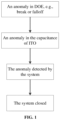
- the DOE of iPhone X has an ITO (Indium Tin Oxide Semiconductor). By monitoring the capacitance of the ITO, it can be determined whether the DOE is abnormal, and then the laser will be turned off to protect the human eyes from direct laser irradiation if an anomaly occurs.
- ITO Indium Tin Oxide Semiconductor
- FIG. 1 The working process of the facial recognition of iPhone X is shown in FIG. 1 , and the details will be described below:
- an ITO detection module is needed, which makes the facial recognition module more complex in structure, larger in size, and increased in cost while the utilization of light energy decreases.
- a collimating lens is arranged downstream of the optical path of the laser light source to collimate the laser.
- a diffractive optical element and an ITO are arranged downstream of the optical path of the collimating lens.
- US patent application US2016/0371845A1 provides a method for projection, which includes projecting a pattern of structured light with a given average intensity onto a scene.
- a sequence of images is captured of the scene while projecting the pattern.
- At least one captured image in the sequence is processed in order to extract a depth map of the scene.
- a condition is identified in the depth map indicative of a fault in projection of the pattern.
- CN patent application CN108376251A discloses a control method of a laser projector.
- the control method of the laser projector comprises the steps: acquiring a projection distance between a target user and a laser projector; according to the projection distance, acquiring an energy density of the laser projector during laser projection based on a preset parameter at a current distance; and on the basis of the energy density and a safety energy threshold, adjusting a preset parameter and controlling the laser projector based on the adjusted parameter.
- CN patent application CN108303835A discloses a structured light projector.
- the structured light projector includes a laser emitter, a collimation element, a diffractive optical element and a light-permeable extension film.
- the laser emitter is used for emitting laser.
- the collimation element is used for collimating laser.
- the diffractive optimal element is used for diffracting laser collimated by the collimation element to form a laser pattern.
- the extension film is arranged on the diffractive optimal element and is combined with the diffractive optimal element, and provides bonding force to the diffractive optimal element when the diffractive optimal element is broken.
- the present invention provides a light projection method and device with safety protection.
- the DOE designed for a divergent light source can be applied to facial recognition, thereby proposing a novel method for safety protection for human eyes, such that an ITO can be removed so as to simplify the structure, decrease the size and reduce costs, and also facilitate efficient utilization of optical energy.
- the present invention provides a light projection method with safety protection, comprising: turning on a light source at a safe power level; using a diffractive optical element to modulate light emitted from the light source so as to project a pattern onto a target surface; acquiring the pattern; and determining whether the pattern is normal and if the pattern is normal, turning on the light source at a rated power level.
- the light projection method further comprises: turning off the light source if the pattern is abnormal, wherein the light source is preferably a laser light source, and the rated power level is preferably higher than the safe power level.
- the light projection method further comprises: calculating the safe power level based on a distance between the light source or the diffractive optical element and the target surface.
- the light projection method further comprises: determining that a fault lies in the light source and/or the diffractive optical element if the pattern is abnormal.
- the light source is configured to emit divergent light of nonplanar waves
- the diffractive optical element is preferably a diffractive optical element that performs optical modulation for the wavefront phase distribution of the incident light field.
- no collimating lens is used to perform collimation processing between the light source and the diffractive optical element, and/or no ITO is used to filter the light modulated by the diffractive optical element.
- the present invention further provides a light projection device, comprising: a light source; a diffractive optical element configured to modulate light emitted from a light source so as to project a pattern onto a target surface; an image acquisition unit configured to acquire the pattern; a processing unit coupled to the image acquisition unit and determining whether the pattern is normal, and if the pattern is normal, turning on the light source at a rated power level.
- the processing unit is configured to turn off the light source if the pattern is determined to be abnormal, wherein the light source is preferably a laser light source.
- the light projection device may further comprise a proximity sensor and/or a distance sensor to measure a distance between the light source or the diffractive optical element and the target surface.
- the processing unit is also configured to calculate the safe power level based on the distance between the light source or the diffractive optical element and the target surface, wherein the rated power level is preferably higher than the safe power level.
- the light projection device further comprises: the processing unit further configured to determine that a fault lies in the light source and/or the diffractive optical element if the pattern is determined to be abnormal.
- the light source is configured to emit divergent light of nonplanar waves
- the diffractive optical element is a diffractive optical element that performs optical modulation for the wavefront phase distribution of the incident light field, wherein preferably no collimating lens is provided between the light source and the diffractive optical element, and/or no ITO is provided on the surface of the diffractive optical element or downstream of the optical path of the diffractive optical element.
- the present invention provides an electronic device, comprising: a body; and a light projection device as described above.
- the electronic device further comprises a proximity sensor and/or a distance sensor capable of detecting a distance from the light projection device, and a processing unit of the light projection device is configured to perform the following operations when the distance is detected to be within a predetermined range: turning on the light source at a safe power level; using a diffractive optical element to modulate light emitted from a light source so as to project a pattern onto a target surface; acquiring the pattern; and determining whether the pattern is normal, and if the pattern is normal, turning on the light source at a rated power level, wherein the rated power level is preferably higher than the safe power level.
- the light projection method and the light projection device according to the embodiments of the present invention can make the optical system smaller in size, simple in structure, and reduced in cost and also improve the utilization of optical energy while ensuring the safety of a user.
- connection may refer to fixed connection, dismountable connection, or integrated connection; also to mechanical connection, electric connection or intercommunication; further to direct connection, or connection by an intermediary medium; or even to internal communication between two elements or interaction between two elements.
- first feature is “above” or “below” a second one, this may cover the direct contact between the first and second features, also cover the contact via another feature there between, instead of the direct contact. Furthermore, if a first feature “above”, “over” or “on the top of” a second one, this may cover that the first feature is right above or on the inclined top of the second feature, or just indicate that the first feature has a horizontal height higher than that of the second feature.
- first feature is "below”, “under” or “on the bottom of” a second feature, this may cover that the first feature is right below and on the inclined bottom of the second feature, or just indicates that the first feature has a horizontal height lower than that of the second feature.
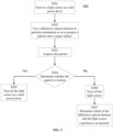
- FIG. 2 illustrates a light projection method 100 according to one embodiment of the present invention, for example, for protecting the eyes of a user from being exposed to strong light so as to prevent damage to the eyes.
- the light projection method 100 of the present invention may also be used for protecting the safety of other objects or surfaces to be illuminated, and this does not impose a limitation on the protection scope of the present invention.
- a light source is turned on at a safe power level in step S101.
- the light source may be a laser light source.
- the protection scope of the present invention is not limited to this, and other types of light sources, for example a LED light source, can also be used.
- the light source for example, is configured to emit divergent light of nonplanar waves, for example spherical waves.
- the safety power level refers to a light source power that is safe for a user or the eyes of the user.
- the safety power level can be determined according to the parameters like light source type and illumination distance. Taking a laser light source as an example, the wavelength of the laser light source can be obtained according to the parameters of the laser light source.
- the threshold R of laser radiation power allowed for an irradiated object for example human eyes
- the safe power level P of the laser light source is calculated assumed that the diffractive optical element falls off, namely under the condition that the laser light source directly irradiates the object (for example the human eyes), and the safe power level P is used as the standard for ensuring the safety of human eyes.
- the illumination distance is taken for reference at the time of calculating the safe power level. Power is related to distance, for example, the working distance from a human face to an optical module can be detected by a proximity sensor and/or distance sensor.
- step S102 light emitted from the light source is modulated by a diffractive optical element so as to project a pattern onto a target surface.
- a diffractive optical element of the present invention can modulate divergent light having nonplanar waves, and is designed with regard to the parameters of a laser irradiating light source to perform optical modulation for the wavefront phase distribution of the incident light field (for example, by means of the iterative analysis of Fourier optical transmission).
- the wavefront of the incident light field may be either planar waves or nonplanar waves (e.g., spherical waves).
- the diffractive optical element is a diffractive optical element optically designed with regard to the parameters such as the wavefront of the laser light source, being used to provide the distribution of the light field as required by the optical system.
- the light field of the laser light source after being optically modulated by the diffractive optical element, transmits regionally at a particular angle.
- step S103 the pattern is acquired.
- the pattern projected onto the target surface for example a human face
- the pattern projected onto the target surface can be collected by a camera or webcam.
- step S104 it is determined whether the pattern is normal, and if so, the light source is turned on at a rated power level.
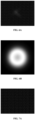
- FIG. 6A shows a pattern of light spots when an anomaly, for example a break, occurs in the diffractive optical element, from which it can be seen that there will be noise in the local area after the diffractive optical element breaks.
- FIG. 6B shows a pattern of light spots when an anomaly, for example a falloff, occurs in the diffractive optical element, in which an abnormally large light spot appears because modulation is not performed by the diffractive optical element.
- FIG. 7A shows a pattern when VCSEL has a bad pixel, in which it can be found that a large gap exists in the dot array.
- FIG. 7B shows a pattern when VCSEL has more bad pixels.
- FIG. 7C shows a pattern when VCSEL is completely off, and the image is all black. After the pattern is acquired, it can be determined whether the projected pattern is normal by means of image processing and analysis.
- the rated power level described herein may be a fixed value, or may be a variable value, for example, a variable value determined by one or more of environment, light intensity, battery, and other factors.
- the power level enables the light source to work normally, it is then regarded as a rated power level.
- the rated power level of the light source when the external light is strong, the rated power level of the light source must be high enough so as to ensure that the pattern projected onto the target surface is clearly visible and can be acquired and processed; and when the external light is weak, the rated power level of the light source can be slightly lower, namely enough to ensure that the projected pattern can be clearly visible and meet the requirements for acquisition and processing.
- the rated power level is higher than the safety power level.
- the present invention is not only limited to this.
- FIG. 3 illustrates a light projection method 200 according to one preferred embodiment of the present invention.
- the steps S201, S202, S203, S204 and S205 in the light projection method 200 correspond to the steps S101, S102, S103 and S 104 in the light projection method of the previous embodiment. These steps will not be repeated below.
- step S204 if it is determined that the image is abnormal in step S204, the light source is turned off (step S206).
- the image is determined to be abnormal, which indicates that a fault takes place in the diffractive optical element and/or the light source, the light source is then turned off such that damage to the user can be completely avoided.
- the light projection method 200 further comprises: determining that the fault lies in the light source and/or the diffractive optical element in step S207, if the pattern is abnormal.
- the pattern when the light source fails and the pattern when the diffractive optical element fails each have their own characteristics.
- the fault can be located so as to determine whether it occurs in the light source or the diffractive optical element or both.
- a database of faults is established according to the patterns of light spots with various faults, then a light spot pattern, after being acquired, is compared with patterns of various faults in the database of faults by the mode recognition method so as to recognize the fault mode and determine the fault location.
- step S206 is performed prior to step S207 as shown in FIG. 3
- the protection scope of the present invention is not limited to the sequence of step S206 and step S207, and the present invention can be performed in the sequence of steps S206 and S207, or in the sequence of steps S207 and S206, or simultaneously. These are all within the protection scope of the claims of the present invention.
- no collimating lens is used to perform collimation processing between the light source and the diffractive optical element.
- the diffractive optical element of the present invention can modulate divergent light, it is then a diffractive optical element designed with regard to the parameters of a laser irradiation light source to perform optical modulation for the wavefront phase distribution of the incident light field, for example, by means of the iterative analysis of Fourier optical transmission.
- the wavefront of the incident light field may be either planar waves or nonplanar waves (e.g., spherical waves).
- the light modulated by the diffractive optical element is not filtered by an ITO in the light projection methods 100 and 200.
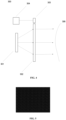
- the light projection device 300 may be used to implement the light projection methods 100 and 200 according to the present invention.
- the light projection device 300 comprises a light source 301, a diffractive optical element 302, an image acquisition unit 303, and a processing unit 304.
- the light source 301 is preferably a laser light source, and surely may also be other types of light sources, for example a LED light source, etc..
- the light source is preferably configured to emit divergent light of nonplanar waves.
- the diffractive optical element 302 can modulate the light emitted from the light source so as to project a pattern onto a target surface 306.
- the target surface 306 may be a human face or other object surfaces, for example.
- the image acquisition unit 303 is, for example, a webcam or camera and can acquire the pattern projected onto the target surface 306.
- the processing unit 304 coupled with the image acquisition unit 303 receives and processes the pattern acquired by the image acquisition unit 303, and determines whether the pattern is normal. If the pattern is normal, the light source 301 is turned on at a rated power level.
- the rated power level is preferably higher than the safe power level. The definitions of the rated power level and the safe power level are recited above and will not be repeated here.
- the processing unit 304 is further configured to turn off the light source if the pattern is determined to be abnormal.
- the pattern projected by the diffractive optical element 302 onto the target surface 306 is abnormal, this indicates that the light source or the diffractive optical element has failed. At this time, it is better to turn off the light source in order to avoid damage caused to the user's eyes or other target surfaces. After the fault is recognized and repaired, the system will be restarted.
- the light projection device 300 may further comprise a proximity sensor (not shown) and/or a distance sensor to measure a distance between the light source or the diffractive optical element and the target surface. After the distance is measured between the light source or the diffractive optical element and the target surface, the processing unit can calculate the safe power level based on the distance. The safe power level calculated in this way is more accurate.
- the proximity sensor and/or the distance sensor can also help to start the light source 301 in time. For example, when a target surface (e.g., a human face) is sensed to be within a certain distance range, this sensing event can trigger the light source 301 to start at the safe power level.
- a pattern is projected onto the target surface 306, the pattern then is acquired by the image acquisition unit 303, and processed by the processing unit 304 to determine whether the pattern is abnormal.
- the processing unit 304 is further configured to determine that the fault lies in the light source and/or the diffractive optical element if the pattern is determined to be abnormal.
- the light source 301 is configured to emit divergent light of nonplanar waves, for example spherical waves
- the diffractive optical element 302 is configured to optically modulate the wavefront phase distribution of the incident light field, wherein preferably no collimating lens is provided between the light source and the diffractive optical element, and/or no ITO is provided on the surface of the diffractive optical element or downstream of the optical path of the diffractive optical element.
- the size of the overall optical system can be made very small. This is a great advantage for increasingly compact electronic devices, especially for mobile phones.
- the present invention also relates to an electronic device, comprising: a body and a light projection device as described above.
- the electronic device may be a mobile phone, PAD, portable computer, face recognition device, monitoring device and other types of electronic devices.
- the light projection device can be installed on the body or physically separated from the body.
- the electronic device of the present invention further comprises a proximity sensor and/or a distance sensor that can detect a distance between the light projection device and the surface of the target object, and the processing unit of the light projection device is configured to perform the following operations when the distance is detected to be within a predetermined range: turning on the light source at a safe power level; using the diffractive optical element to modulate light emitted from the light source so as to project a pattern onto the target surface; acquiring the pattern; determining whether the pattern is normal, and if so, turning on the light source at a rated power level.
- the rated power level is preferably higher than the safe power level.
- the predetermined range mentioned above is 200-700mm, for example.
- the user may primarily select hardware and/or firmware media; if flexibility is valued, the user may take a software implementation mode as the first choice; or alternatively, the user can select some combination of hardware, software and/or firmware.
- the mechanism of the subject matter described herein can be distributed as various forms of program products, and the illustrative examples of the subject matter described herein are applicable regardless of the specific types of the signal-carrying media actually used to implement the distribution.
- Examples of the signal-carrying media include but are not limited to the following: recordable media such as floppy disk, hard disk drive, compact disk (CD), digital video disk (DVD), digital tape, computer memory, etc.; and transmission-type media such as digital and/or analog communication media (e.g., optical fiber cable, waveguide, wired communication link, wireless communication link, etc.).
- a typical data processing system generally includes one or more of the following: a system unit housing, a video display device, a memory such as volatile and non-volatile memory, a processor such as a microprocessor and a digital signal processor, a computing entity such as an operating system, a driver, a graphical user interface, and an application program, one or more interactive devices such as a touch pad or touch screen, and/or a control system comprising a feedback loop and a control motor (e.g., feedback for sensing position and/or speed; and a control motor for moving and/or adjusting components and/or quantities).
- a typical data processing system may be implemented using any suitable commercially available component, such as those common in data computing/communication and/or network computing/communication systems.
- any two components associated with each other as so can be further regarded as “operatively connected” or “operatively coupled” with each other to achieve the desired function
- any two components associable with each other as so can be further regarded as "capable of being operatively coupled” with each other to achieve the desired function.
- operable coupling include, but are not limited to, components that can be physically combined and/or physically interacted, and/or components that can interact wirelessly and/or wirelessly, and/or components that interact logically and/or can interact logically.
Landscapes
- Physics & Mathematics (AREA)
- General Physics & Mathematics (AREA)
- Engineering & Computer Science (AREA)
- Optics & Photonics (AREA)
- Computer Vision & Pattern Recognition (AREA)
- Theoretical Computer Science (AREA)
- Multimedia (AREA)
- Oral & Maxillofacial Surgery (AREA)
- Human Computer Interaction (AREA)
- General Health & Medical Sciences (AREA)
- Health & Medical Sciences (AREA)
- Projection Apparatus (AREA)
- Semiconductor Lasers (AREA)
- Length Measuring Devices By Optical Means (AREA)
Claims (12)
- Lichtprojektionsverfahren (100, 200) mit Sicherheitsschutz, umfassend:Einschalten einer Lichtquelle (301) bei einem sicheren Leistungspegel (S101, S201);Verwenden eines optischen Beugungselements (302), das von der Lichtquelle (301) abgestrahltes Licht moduliert, um ein Muster auf eine Zieloberfläche (306) zu projizieren (S102, S202); undErfassen des Musters (S103, S203);dadurch gekennzeichnet, dass das Lichtprojektionsverfahren (100, 200) ferner umfasst:
Bestimmen, ob das Muster normal ist (S104, S204), und wenn das Muster normal ist, Einschalten der Lichtquelle (301) bei einem Bemessungsleistungspegel (S105, S205), wobei das Bestimmen, ob das Muster normal ist, umfasst: Vergleichen des Musters mit Mustern von verschiedenen Fehlern in einer Datenbank mit Fehlern, um einen Fehlermodus zu erkennen und eine Fehlerposition zu bestimmen, wobei die Fehlerposition die Lichtquelle oder das optische Beugungselement oder beide sind, wobei die Datenbank mit Fehlern im Voraus anhand von Mustern von Lichtpunkten mit verschiedenen Fehler erstellt wird. - Lichtprojektionsverfahren nach Anspruch 1, ferner umfassend: Ausschalten der Lichtquelle (301), wenn das Muster anormal ist (S206), wobei die Lichtquelle (301) vorzugsweise eine Laserlichtquelle ist und der Bemessungsleistungspegel vorzugsweise höher als der sichere Leistungspegel ist.
- Lichtprojektionsverfahren nach den Ansprüchen 1 oder 2, ferner umfassend: Berechnen des sicheren Leistungspegels auf Grundlage eines Abstands zwischen der Lichtquelle (301) oder dem optischen Beugungselement (302) und der Zieloberfläche (306).
- Lichtprojektionsverfahren nach den Ansprüchen 1 oder 2, ferner umfassend: Bestimmen, dass ein Fehler in der Lichtquelle (301) und/oder dem optischen Beugungselement (302) vorliegt, wenn das Muster anormal ist (S207).
- Lichtprojektionsverfahren nach den Ansprüchen 1 oder 2, wobei die Lichtquelle (301) dazu konfiguriert ist, divergierendes Licht mit nichtplanaren Wellen abzustrahlen, und das optische Beugungselement (302) ein optisches Beugungselement (302) ist, das eine optische Modulation für die Wellenfrontphasenverteilung des einfallenden Lichtfelds durchführt.
- Lichtprojektionsverfahren nach den Ansprüchen 1 oder 2, wobei keine Kollimationslinse verwendet wird, um eine Kollimationsverarbeitung zwischen der Lichtquelle (301) und dem optischen Beugungselement (302) durchzuführen, und/oder kein ITO verwendet wird, um das durch das optische Beugungselement (302) modulierte Licht zu filtern.
- Lichtprojektionsvorrichtung (300), umfassend:eine Lichtquelle (301), die dazu konfiguriert ist, bei einem sicheren Leistungspegel eingeschaltet zu werden;ein optisches Beugungselement (302), das dazu konfiguriert ist, von der Lichtquelle (301) abgestrahltes Licht zu modulieren, um ein Muster auf eine Zieloberfläche (306) zu projizieren; undeine Bilderfassungseinheit (303), die dazu konfiguriert ist, das Muster zu erfassen;dadurch gekennzeichnet, dass die Lichtprojektionsvorrichtung (300) ferner umfasst:
eine Verarbeitungseinheit (304), die an die Bilderfassungseinheit (303) gekoppelt ist und bestimmt, ob das Muster normal ist, und wenn das Muster normal ist, die Lichtquelle (301) bei einem Bemessungsleistungspegel einschaltet, wobei das Bestimmen, ob das Muster normal ist, umfasst: Vergleichen des Musters mit Mustern von verschiedenen Fehlern in einer Datenbank mit Fehlern, um einen Fehlermodus zu erkennen und eine Fehlerposition zu bestimmen, wobei die Fehlerposition die Lichtquelle oder das optische Beugungselement oder beide sind, wobei die Datenbank mit Fehlern im Voraus anhand von Mustern von Lichtpunkten mit verschiedenen Fehler erstellt wird. - Lichtprojektionsvorrichtung (300) nach Anspruch 7, wobei die Verarbeitungseinheit dazu konfiguriert ist, die Lichtquelle (301) auszuschalten, wenn bestimmt wird, dass das Muster anormal ist, wobei die Lichtquelle (301) vorzugsweise eine Laserlichtquelle ist; wobei die Lichtprojektionsvorrichtung (300) vorzugsweise ferner einen Näherungssensor und/oder einen Abstandssensor zum Messen eines Abstands zwischen der Lichtquelle (301) oder dem optischen Beugungselement (302) und der Zieloberfläche (306) zu messen; wobei die Verarbeitungseinheit außerdem dazu konfiguriert ist, den sicheren Leistungspegel auf Grundlage eines Abstands zwischen der Lichtquelle (301) oder dem optischen Beugungselement (302) und der Zieloberfläche (306) zu berechnen; und wobei der Bemessungsleistungspegel vorzugsweise höher als der sichere Leistungspegel ist.
- Lichtprojektionsvorrichtung (300) nach den Ansprüchen 7 oder 8, wobei die Verarbeitungseinheit ferner dazu konfiguriert ist, zu bestimmen, dass ein Fehler bei der Lichtquelle (301) und/oder dem optischen Beugungselement (302) vorliegt, wenn bestimmt wird, dass das Muster anormal ist.
- Lichtprojektionsvorrichtung (300) nach den Ansprüchen 7 oder 8, wobei die Lichtquelle (301) dazu konfiguriert ist, divergierendes Licht mit nichtplanaren Wellen abzustrahlen, und das optische Beugungselement (302) ein optisches Beugungselement (302) ist, das eine optische Modulation für die Wellenfrontphasenverteilung des einfallenden Lichtfelds durchführt, wobei vorzugsweise keine Kollimationslinse zwischen der Lichtquelle (301) und dem optischen Beugungselement (302) bereitgestellt ist und/oder kein ITO auf der Oberfläche des optischen Beugungselements (302) oder dem optischen Weg des optischen Beugungselements (302) nachgelagert bereitgestellt ist.
- Elektronische Vorrichtung, umfassend:einen Körper; unddie Lichtprojektionsvorrichtung (300) nach einem der Ansprüche 7 bis 10.
- Elektronische Vorrichtung nach Anspruch 11, ferner umfassend einen Näherungssensor und/oder einen Entfernungssensor, die einen Abstand von der Lichtprojektionsvorrichtung (300) erkennen können, und eine Verarbeitungseinheit der Lichtprojektionsvorrichtung (300), die dazu konfiguriert ist, die folgende Vorgänge durchzuführen, wenn erkannt wird, dass das Abstand innerhalb eines vorgegebenen Bereichs liegt:Einschalten der Lichtquelle (301) bei einem sicheren Leistungspegel;Verwenden eines optischen Beugungselements (302), das von der Lichtquelle (301) abgestrahltes Licht moduliert, um ein Muster auf eine Zieloberfläche (306) zu projizieren;Erfassen des Musters;Bestimmen, ob das Muster normal ist, und wenn das Muster normal ist, Einschalten der Lichtquelle (301) bei einem Bemessungsleistungspegel, wobei der Bemessungsleistungspegel vorzugsweise höher als der sichere Leistungspegel ist.
Applications Claiming Priority (5)
| Application Number | Priority Date | Filing Date | Title |
|---|---|---|---|
| CN201920186585 | 2019-02-01 | ||
| CN201910105589 | 2019-02-01 | ||
| CN201910113196.8A CN109932828B (zh) | 2019-02-01 | 2019-02-13 | 光投射方法及光投射装置 |
| CN201920194700.7U CN209728345U (zh) | 2019-02-01 | 2019-02-13 | 光投射装置和电子设备 |
| PCT/CN2020/071356 WO2020156096A1 (zh) | 2019-02-01 | 2020-01-10 | 光投射方法及光投射装置 |
Publications (4)
| Publication Number | Publication Date |
|---|---|
| EP3919964A1 EP3919964A1 (de) | 2021-12-08 |
| EP3919964A4 EP3919964A4 (de) | 2022-11-02 |
| EP3919964C0 EP3919964C0 (de) | 2024-10-23 |
| EP3919964B1 true EP3919964B1 (de) | 2024-10-23 |
Family
ID=66985590
Family Applications (1)
| Application Number | Title | Priority Date | Filing Date |
|---|---|---|---|
| EP20749027.7A Active EP3919964B1 (de) | 2019-02-01 | 2020-01-10 | Lichtprojektionsverfahren und lichtprojektionsvorrichtung |
Country Status (4)
| Country | Link |
|---|---|
| US (1) | US11774238B2 (de) |
| EP (1) | EP3919964B1 (de) |
| CN (2) | CN209728345U (de) |
| WO (1) | WO2020156096A1 (de) |
Families Citing this family (11)
| Publication number | Priority date | Publication date | Assignee | Title |
|---|---|---|---|---|
| CN209728345U (zh) | 2019-02-01 | 2019-12-03 | 杭州驭光光电科技有限公司 | 光投射装置和电子设备 |
| US12265232B2 (en) * | 2019-02-14 | 2025-04-01 | Hangzhou Uphoton Optoelectronics Technology Co., Ltd. | Beam-splitting optical module and manufacturing method thereof |
| CN110705417A (zh) * | 2019-09-24 | 2020-01-17 | 杭州驭光光电科技有限公司 | 人头计数方法及光投射装置 |
| CN110717901B (zh) * | 2019-09-27 | 2023-05-26 | 深圳市安思疆科技有限公司 | 一种基于光标的软件场景doe性能评估方法 |
| CN110749948B (zh) * | 2019-11-15 | 2025-10-21 | 嘉兴驭光光电科技有限公司 | 衍射光学元件、包括其的光学组件以及基准线投射装置 |
| TWI801858B (zh) * | 2020-09-29 | 2023-05-11 | 仁寶電腦工業股份有限公司 | 具有輔助照明功能的電子裝置及其操作方法 |
| CN113052155B (zh) * | 2021-02-03 | 2024-04-02 | 深圳赋能光达科技有限公司 | 光源亮度调节器、结构光投射器、身份识别装置及电子设备 |
| CN113807172B (zh) * | 2021-08-11 | 2022-10-18 | 荣耀终端有限公司 | 一种人脸识别方法和装置 |
| CN115705726B (zh) * | 2021-08-11 | 2025-10-24 | 荣耀终端股份有限公司 | 一种人脸识别方法和装置 |
| CN115436963A (zh) * | 2022-09-01 | 2022-12-06 | 深圳市汇顶科技股份有限公司 | 一种飞行时差测距模组及其的异常检测方法及电子设备 |
| CN121173944A (zh) * | 2024-06-18 | 2025-12-19 | 腾讯科技(深圳)有限公司 | 视觉信息采集设备的自检方法及相关设备 |
Family Cites Families (17)
| Publication number | Priority date | Publication date | Assignee | Title |
|---|---|---|---|---|
| DE102009031732B3 (de) * | 2009-07-04 | 2010-11-25 | Sick Ag | Entfernungsmessender optoelektronischer Sensor |
| US8330134B2 (en) * | 2009-09-14 | 2012-12-11 | Microsoft Corporation | Optical fault monitoring |
| DE102010037744B3 (de) * | 2010-09-23 | 2011-12-08 | Sick Ag | Optoelektronischer Sensor |
| US9528906B1 (en) | 2013-12-19 | 2016-12-27 | Apple Inc. | Monitoring DOE performance using total internal reflection |
| US11054664B2 (en) * | 2015-06-18 | 2021-07-06 | Apple Inc. | Monitoring DOE performance using software scene evaluation |
| WO2017113286A1 (zh) * | 2015-12-31 | 2017-07-06 | 深圳先进技术研究院 | 一种认证方法及装置 |
| CN108376251B (zh) * | 2018-02-27 | 2020-04-17 | Oppo广东移动通信有限公司 | 控制方法、控制装置、终端、计算机设备和存储介质 |
| CN113156742B (zh) | 2018-02-27 | 2022-05-20 | Oppo广东移动通信有限公司 | 结构光投射器及其控制方法、深度相机和电子装置 |
| CN108760245B (zh) * | 2018-04-28 | 2019-07-23 | Oppo广东移动通信有限公司 | 光学元件检测方法和装置、电子设备、可读存储介质 |
| CN108508620B (zh) * | 2018-03-12 | 2020-03-06 | Oppo广东移动通信有限公司 | 激光投射模组的检测方法、检测装置和电子装置 |
| CN108445643B (zh) * | 2018-03-12 | 2021-05-14 | Oppo广东移动通信有限公司 | 结构光投射模组及其检测方法与装置、图像获取结构和电子装置 |
| CN108490629B (zh) * | 2018-03-12 | 2020-03-27 | Oppo广东移动通信有限公司 | 结构光投射器及其检测方法与装置、图像获取装置和电子设备 |
| CN108508624B (zh) * | 2018-03-12 | 2020-01-10 | Oppo广东移动通信有限公司 | 激光投射模组及其检测方法与装置、深度相机和电子装置 |
| US10593055B2 (en) * | 2018-03-23 | 2020-03-17 | Capsovision Inc | Method and apparatus for capturing images and associated 3D model based on a single image sensor and structured-light patterns in the visible spectrum |
| WO2019223002A1 (zh) * | 2018-05-25 | 2019-11-28 | 深圳阜时科技有限公司 | 一种结构光检测装置及检测方法、身份识别装置及电子设备 |
| CN109521627B (zh) * | 2018-06-21 | 2021-04-23 | 昆山丘钛微电子科技有限公司 | 光学投影模组及其控制方法 |
| CN209728345U (zh) * | 2019-02-01 | 2019-12-03 | 杭州驭光光电科技有限公司 | 光投射装置和电子设备 |
-
2019
- 2019-02-13 CN CN201920194700.7U patent/CN209728345U/zh active Active
- 2019-02-13 CN CN201910113196.8A patent/CN109932828B/zh active Active
-
2020
- 2020-01-10 US US17/426,540 patent/US11774238B2/en active Active
- 2020-01-10 EP EP20749027.7A patent/EP3919964B1/de active Active
- 2020-01-10 WO PCT/CN2020/071356 patent/WO2020156096A1/zh not_active Ceased
Also Published As
| Publication number | Publication date |
|---|---|
| CN109932828A (zh) | 2019-06-25 |
| WO2020156096A1 (zh) | 2020-08-06 |
| CN209728345U (zh) | 2019-12-03 |
| US20220090914A1 (en) | 2022-03-24 |
| EP3919964A1 (de) | 2021-12-08 |
| US11774238B2 (en) | 2023-10-03 |
| EP3919964A4 (de) | 2022-11-02 |
| EP3919964C0 (de) | 2024-10-23 |
| CN109932828B (zh) | 2024-10-01 |
Similar Documents
| Publication | Publication Date | Title |
|---|---|---|
| EP3919964B1 (de) | Lichtprojektionsverfahren und lichtprojektionsvorrichtung | |
| US12406384B2 (en) | Depth measurement through display | |
| US8330720B2 (en) | Optical navigation system and method for performing self-calibration on the system using a calibration cover | |
| US8492696B2 (en) | Optical projector with beam monitor including mapping apparatus capturing image of pattern projected onto an object | |
| US10230929B2 (en) | Systems, devices, and methods for laser projectors | |
| US9185352B1 (en) | Mobile eye tracking system | |
| JP2011507336A (ja) | イメージング装置の制御のための近接検知 | |
| US20230403906A1 (en) | Depth measurement through display | |
| US11973314B2 (en) | Light-source drive device and light-emitting device | |
| AU2008308677A1 (en) | Combined object capturing system and display device and associated method | |
| US9063001B2 (en) | Optical fault monitoring | |
| KR20160137313A (ko) | 3차원 카메라를 이용한 차륜 정렬 요소 측정용 타겟보드 및 이를 이용한 차륜 정렬 요소 측정 시스템 | |
| CN105319606A (zh) | 多光轴光电传感器系统 | |
| CN108508620A (zh) | 激光投射模组的检测方法、检测装置和电子装置 | |
| JP6731460B2 (ja) | プロジェクタを制御する方法及び関連する電子デバイス | |
| CN110705417A (zh) | 人头计数方法及光投射装置 | |
| CN108445643B (zh) | 结构光投射模组及其检测方法与装置、图像获取结构和电子装置 | |
| KR20210078114A (ko) | 광원 구동 제어장치 및 방법 | |
| US9207809B2 (en) | Optical touch system and optical touch control method | |
| JP2004185283A (ja) | 光学式座標入力装置 | |
| US20240288699A1 (en) | Electronic Devices with Nose Tracking Sensors | |
| JP4940591B2 (ja) | 画像表示装置及びレーザ機器 | |
| CN111857411A (zh) | 投影设备的红外触控功能控制方法、投影设备和存储介质 |
Legal Events
| Date | Code | Title | Description |
|---|---|---|---|
| STAA | Information on the status of an ep patent application or granted ep patent |
Free format text: STATUS: THE INTERNATIONAL PUBLICATION HAS BEEN MADE |
|
| PUAI | Public reference made under article 153(3) epc to a published international application that has entered the european phase |
Free format text: ORIGINAL CODE: 0009012 |
|
| STAA | Information on the status of an ep patent application or granted ep patent |
Free format text: STATUS: REQUEST FOR EXAMINATION WAS MADE |
|
| 17P | Request for examination filed |
Effective date: 20210809 |
|
| AK | Designated contracting states |
Kind code of ref document: A1 Designated state(s): AL AT BE BG CH CY CZ DE DK EE ES FI FR GB GR HR HU IE IS IT LI LT LU LV MC MK MT NL NO PL PT RO RS SE SI SK SM TR |
|
| DAV | Request for validation of the european patent (deleted) | ||
| DAX | Request for extension of the european patent (deleted) | ||
| A4 | Supplementary search report drawn up and despatched |
Effective date: 20220929 |
|
| RIC1 | Information provided on ipc code assigned before grant |
Ipc: G06V 40/16 20220101ALI20220923BHEP Ipc: G06V 10/141 20220101ALI20220923BHEP Ipc: G01B 11/02 20060101ALI20220923BHEP Ipc: G01B 11/25 20060101ALI20220923BHEP Ipc: G02B 27/42 20060101AFI20220923BHEP |
|
| GRAP | Despatch of communication of intention to grant a patent |
Free format text: ORIGINAL CODE: EPIDOSNIGR1 |
|
| STAA | Information on the status of an ep patent application or granted ep patent |
Free format text: STATUS: GRANT OF PATENT IS INTENDED |
|
| GRAS | Grant fee paid |
Free format text: ORIGINAL CODE: EPIDOSNIGR3 |
|
| INTG | Intention to grant announced |
Effective date: 20240816 |
|
| GRAA | (expected) grant |
Free format text: ORIGINAL CODE: 0009210 |
|
| STAA | Information on the status of an ep patent application or granted ep patent |
Free format text: STATUS: THE PATENT HAS BEEN GRANTED |
|
| AK | Designated contracting states |
Kind code of ref document: B1 Designated state(s): AL AT BE BG CH CY CZ DE DK EE ES FI FR GB GR HR HU IE IS IT LI LT LU LV MC MK MT NL NO PL PT RO RS SE SI SK SM TR |
|
| REG | Reference to a national code |
Ref country code: GB Ref legal event code: FG4D |
|
| REG | Reference to a national code |
Ref country code: CH Ref legal event code: EP |
|
| REG | Reference to a national code |
Ref country code: DE Ref legal event code: R096 Ref document number: 602020039918 Country of ref document: DE |
|
| REG | Reference to a national code |
Ref country code: IE Ref legal event code: FG4D |
|
| U01 | Request for unitary effect filed |
Effective date: 20241111 |
|
| U07 | Unitary effect registered |
Designated state(s): AT BE BG DE DK EE FI FR IT LT LU LV MT NL PT RO SE SI Effective date: 20241119 |
|
| U20 | Renewal fee for the european patent with unitary effect paid |
Year of fee payment: 6 Effective date: 20250108 |
|
| PG25 | Lapsed in a contracting state [announced via postgrant information from national office to epo] |
Ref country code: IS Free format text: LAPSE BECAUSE OF FAILURE TO SUBMIT A TRANSLATION OF THE DESCRIPTION OR TO PAY THE FEE WITHIN THE PRESCRIBED TIME-LIMIT Effective date: 20250223 Ref country code: HR Free format text: LAPSE BECAUSE OF FAILURE TO SUBMIT A TRANSLATION OF THE DESCRIPTION OR TO PAY THE FEE WITHIN THE PRESCRIBED TIME-LIMIT Effective date: 20241023 |
|
| PG25 | Lapsed in a contracting state [announced via postgrant information from national office to epo] |
Ref country code: ES Free format text: LAPSE BECAUSE OF FAILURE TO SUBMIT A TRANSLATION OF THE DESCRIPTION OR TO PAY THE FEE WITHIN THE PRESCRIBED TIME-LIMIT Effective date: 20241023 |
|
| PG25 | Lapsed in a contracting state [announced via postgrant information from national office to epo] |
Ref country code: NO Free format text: LAPSE BECAUSE OF FAILURE TO SUBMIT A TRANSLATION OF THE DESCRIPTION OR TO PAY THE FEE WITHIN THE PRESCRIBED TIME-LIMIT Effective date: 20250123 |
|
| PG25 | Lapsed in a contracting state [announced via postgrant information from national office to epo] |
Ref country code: GR Free format text: LAPSE BECAUSE OF FAILURE TO SUBMIT A TRANSLATION OF THE DESCRIPTION OR TO PAY THE FEE WITHIN THE PRESCRIBED TIME-LIMIT Effective date: 20250124 |
|
| PG25 | Lapsed in a contracting state [announced via postgrant information from national office to epo] |
Ref country code: PL Free format text: LAPSE BECAUSE OF FAILURE TO SUBMIT A TRANSLATION OF THE DESCRIPTION OR TO PAY THE FEE WITHIN THE PRESCRIBED TIME-LIMIT Effective date: 20241023 |
|
| PG25 | Lapsed in a contracting state [announced via postgrant information from national office to epo] |
Ref country code: RS Free format text: LAPSE BECAUSE OF FAILURE TO SUBMIT A TRANSLATION OF THE DESCRIPTION OR TO PAY THE FEE WITHIN THE PRESCRIBED TIME-LIMIT Effective date: 20250123 |
|
| PG25 | Lapsed in a contracting state [announced via postgrant information from national office to epo] |
Ref country code: SM Free format text: LAPSE BECAUSE OF FAILURE TO SUBMIT A TRANSLATION OF THE DESCRIPTION OR TO PAY THE FEE WITHIN THE PRESCRIBED TIME-LIMIT Effective date: 20241023 |
|
| PG25 | Lapsed in a contracting state [announced via postgrant information from national office to epo] |
Ref country code: SK Free format text: LAPSE BECAUSE OF FAILURE TO SUBMIT A TRANSLATION OF THE DESCRIPTION OR TO PAY THE FEE WITHIN THE PRESCRIBED TIME-LIMIT Effective date: 20241023 |
|
| PG25 | Lapsed in a contracting state [announced via postgrant information from national office to epo] |
Ref country code: CZ Free format text: LAPSE BECAUSE OF FAILURE TO SUBMIT A TRANSLATION OF THE DESCRIPTION OR TO PAY THE FEE WITHIN THE PRESCRIBED TIME-LIMIT Effective date: 20241023 |
|
| PLBE | No opposition filed within time limit |
Free format text: ORIGINAL CODE: 0009261 |
|
| REG | Reference to a national code |
Ref country code: CH Ref legal event code: PL |
|
| STAA | Information on the status of an ep patent application or granted ep patent |
Free format text: STATUS: NO OPPOSITION FILED WITHIN TIME LIMIT |
|
| PG25 | Lapsed in a contracting state [announced via postgrant information from national office to epo] |
Ref country code: MC Free format text: LAPSE BECAUSE OF FAILURE TO SUBMIT A TRANSLATION OF THE DESCRIPTION OR TO PAY THE FEE WITHIN THE PRESCRIBED TIME-LIMIT Effective date: 20241023 |
|
| GBPC | Gb: european patent ceased through non-payment of renewal fee |
Effective date: 20250123 |
|
| 26N | No opposition filed |
Effective date: 20250724 |
|
| PG25 | Lapsed in a contracting state [announced via postgrant information from national office to epo] |
Ref country code: GB Free format text: LAPSE BECAUSE OF NON-PAYMENT OF DUE FEES Effective date: 20250123 |
|
| PG25 | Lapsed in a contracting state [announced via postgrant information from national office to epo] |
Ref country code: CH Free format text: LAPSE BECAUSE OF NON-PAYMENT OF DUE FEES Effective date: 20250131 |
|
| PG25 | Lapsed in a contracting state [announced via postgrant information from national office to epo] |
Ref country code: IE Free format text: LAPSE BECAUSE OF NON-PAYMENT OF DUE FEES Effective date: 20250110 |
|
| U20 | Renewal fee for the european patent with unitary effect paid |
Year of fee payment: 7 Effective date: 20260108 |