EP3923005B1 - Auto-test d'un détecteur de cycle de service - Google Patents
Auto-test d'un détecteur de cycle de service Download PDFInfo
- Publication number
- EP3923005B1 EP3923005B1 EP20305638.7A EP20305638A EP3923005B1 EP 3923005 B1 EP3923005 B1 EP 3923005B1 EP 20305638 A EP20305638 A EP 20305638A EP 3923005 B1 EP3923005 B1 EP 3923005B1
- Authority
- EP
- European Patent Office
- Prior art keywords
- clock signal
- duty cycle
- output
- generator
- circuit
- Prior art date
- Legal status (The legal status is an assumption and is not a legal conclusion. Google has not performed a legal analysis and makes no representation as to the accuracy of the status listed.)
- Active
Links
Images


Classifications
-
- H—ELECTRICITY
- H03—ELECTRONIC CIRCUITRY
- H03K—PULSE TECHNIQUE
- H03K5/00—Manipulating of pulses not covered by one of the other main groups of this subclass
- H03K5/19—Monitoring patterns of pulse trains
-
- G—PHYSICS
- G01—MEASURING; TESTING
- G01R—MEASURING ELECTRIC VARIABLES; MEASURING MAGNETIC VARIABLES
- G01R31/00—Arrangements for testing electric properties; Arrangements for locating electric faults; Arrangements for electrical testing characterised by what is being tested not provided for elsewhere
- G01R31/28—Testing of electronic circuits, e.g. by signal tracer
- G01R31/317—Testing of digital circuits
- G01R31/31708—Analysis of signal quality
-
- G—PHYSICS
- G01—MEASURING; TESTING
- G01R—MEASURING ELECTRIC VARIABLES; MEASURING MAGNETIC VARIABLES
- G01R31/00—Arrangements for testing electric properties; Arrangements for locating electric faults; Arrangements for electrical testing characterised by what is being tested not provided for elsewhere
- G01R31/28—Testing of electronic circuits, e.g. by signal tracer
- G01R31/317—Testing of digital circuits
- G01R31/31727—Clock circuits aspects, e.g. test clock circuit details, timing aspects for signal generation, circuits for testing clocks
-
- G—PHYSICS
- G01—MEASURING; TESTING
- G01R—MEASURING ELECTRIC VARIABLES; MEASURING MAGNETIC VARIABLES
- G01R29/00—Arrangements for measuring or indicating electric quantities not covered by groups G01R19/00 - G01R27/00
- G01R29/02—Measuring characteristics of individual pulses, e.g. deviation from pulse flatness, rise time or duration
-
- G—PHYSICS
- G01—MEASURING; TESTING
- G01S—RADIO DIRECTION-FINDING; RADIO NAVIGATION; DETERMINING DISTANCE OR VELOCITY BY USE OF RADIO WAVES; LOCATING OR PRESENCE-DETECTING BY USE OF THE REFLECTION OR RERADIATION OF RADIO WAVES; ANALOGOUS ARRANGEMENTS USING OTHER WAVES
- G01S7/00—Details of systems according to groups G01S13/00, G01S15/00, G01S17/00
- G01S7/02—Details of systems according to groups G01S13/00, G01S15/00, G01S17/00 of systems according to group G01S13/00
- G01S7/40—Means for monitoring or calibrating
-
- G—PHYSICS
- G01—MEASURING; TESTING
- G01S—RADIO DIRECTION-FINDING; RADIO NAVIGATION; DETERMINING DISTANCE OR VELOCITY BY USE OF RADIO WAVES; LOCATING OR PRESENCE-DETECTING BY USE OF THE REFLECTION OR RERADIATION OF RADIO WAVES; ANALOGOUS ARRANGEMENTS USING OTHER WAVES
- G01S7/00—Details of systems according to groups G01S13/00, G01S15/00, G01S17/00
- G01S7/02—Details of systems according to groups G01S13/00, G01S15/00, G01S17/00 of systems according to group G01S13/00
- G01S7/40—Means for monitoring or calibrating
- G01S7/4004—Means for monitoring or calibrating of parts of a radar system
- G01S7/4008—Means for monitoring or calibrating of parts of a radar system of transmitters
-
- G—PHYSICS
- G01—MEASURING; TESTING
- G01S—RADIO DIRECTION-FINDING; RADIO NAVIGATION; DETERMINING DISTANCE OR VELOCITY BY USE OF RADIO WAVES; LOCATING OR PRESENCE-DETECTING BY USE OF THE REFLECTION OR RERADIATION OF RADIO WAVES; ANALOGOUS ARRANGEMENTS USING OTHER WAVES
- G01S7/00—Details of systems according to groups G01S13/00, G01S15/00, G01S17/00
- G01S7/02—Details of systems according to groups G01S13/00, G01S15/00, G01S17/00 of systems according to group G01S13/00
- G01S7/40—Means for monitoring or calibrating
- G01S7/4004—Means for monitoring or calibrating of parts of a radar system
- G01S7/4021—Means for monitoring or calibrating of parts of a radar system of receivers
-
- H—ELECTRICITY
- H03—ELECTRONIC CIRCUITRY
- H03K—PULSE TECHNIQUE
- H03K3/00—Circuits for generating electric pulses; Monostable, bistable or multistable circuits
- H03K3/01—Details
- H03K3/017—Adjustment of width or dutycycle of pulses
Definitions
- the disclosure relates to apparatus and methods for self-testing of a duty cycle detector.
- Modem radar applications such as in automotive safety and guidance systems, require accurate duty cycle detectors for monitoring whether correct clock signals are being provided. Signals having out-of-specification duty cycle values can result in degraded system performance and misinterpreted data outputs. It is therefore important that any duty cycle detector can be determined to be functional and of sufficient accuracy prior to operation of the associated radar transceiver.
- WO 2010/018544 A1 and WO 2007/010452 A2 disclose testing of a transmission and reception system, in which a test signal is sent from a transmitter to a receiver, the received signal is analyzed, a duty cycle relationship is varied between the test signal and a timing signal used by the receiver and the effect of the duty cycle variation analyzed as a form of embedded jitter insertion.
- EP 1475907 A1 discloses a method of testing an optical electrical converter, in which an input signal is applied with a parameter that is out of a specified application range defined by normal operational characteristics of the converter and an electrical output signal of the converter is evaluated in response to the input signal to determine the result of the testing procedure.
- US 2002/0079941 A1 discloses a duty cycle correction circuit that reduces distortion caused by mismatched transistor pairs.
- US 7,062,692 discloses a method of duty cycle determination and adjustment, in which an output signal is sampled and provided to a duty cycle check circuitry which characterizes the duty cycle of the sampled output signal.
- a circuit as defined in the independent claim 1 relates to a method as defined in the independent claim 11. Additionally, the invention relates to a radar transceiver, as defined in claims 9 and 10, comprising the circuit of the invention. Further embodiments of the invention are defined in the corresponding dependent claims 2-8 and 12-14.
- the description and the drawing also present additional aspects, non-claimed embodiments, examples, and implementations for the better understanding of the claimed embodiments defined in the appended claims. In this respect, the scope of the invention is defined by the claims.
- a duty cycle detector By generating a signal with a deliberately out-of-specification duty cycle, a duty cycle detector can be tested to determine whether it is correctly working and, if not, a flag can be generated as an output of a system self-test routine.
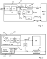
- FIG 1 illustrates a clock signal module 101 and master control unit (MCU) 102, in which clock signals 103, 104 are generated by a reference phase locked loop (PLL) module 105.
- the clock signal module 101 may for example form part of a radar transceiver, in which the clock signals are used to drive operation of various other components of a transmitter and/or receiver part of the transceiver.
- the reference PLL module 105 receives an input clock signal at a crystal frequency and generates a clock signal 113 with a clock PLL 111, which is provided to a clock signal divider 112.
- the clock signal divider 112 generates the clock signals 103, 104, which are provided to an analogue to digital converter (ADC) 106 and main PLL 107.
- ADC analogue to digital converter
- the clock signals 103, 104 are monitored by first and second duty cycle detectors 108, 109. Each detector 108, 109 provides an output flag to a safety controller 110 if an error is detected in the respective clock signal 103, 104.
- the safety controller 110 provides an error flag to the MCU 102 indicating which clock signal 103, 104 is out of range. An out of range clock signal will mean that data dependent on the clock signal is probably corrupted, or a function is not operating as expected or with degraded performance. The data processed for any frame in which a flag is raised should therefore be discarded at the application level.
- a problem with the above described clock signal module is that an out-of-specification duty cycle in any of the clock signals will only be detected if the duty cycle detectors 108, 109 are operating correctly. If either of the detectors 109, 109 is not functional, errors in the duty cycle of the respective clock signal 103, 104 will not be detected and errors will then result in data processed dependent on these clock signals.
- FIG 2 illustrates a clock signal module 201 configured to address the above-mentioned problem.
- a clock signal generator 205 is arranged to generate a clock signal 203 having a defined duty cycle.
- the clock signal 203 is provided to a block or function 206 (such as the ADC 106 or Main PLL 107 shown in Figure 1 ) that requires the clock signal 203 to operate.
- the clock signal generator 205 comprises a voltage controlled oscillator (VCO) 211 and divider 212.
- the clock signal generator 205 comprises a duty cycle generator 213, which is arranged to provide the output clock signal 203 with a predetermined duty cycle. Operation of the duty cycle generator 213 is controlled by a digital controller 214, which incorporates a built-in self-test (BIST) mode 215.
- BIST built-in self-test
- a duty cycle select signal 216 is provided to the duty cycle generator 213 to select one of a plurality of available duty cycles to be applied to the clock signal 203.
- a duty cycle detector 208 monitors the clock signal 203 and provides a flag signal to a fault collection central unit (FCCU) 210 in the event that an out-of-range duty cycle is detected in the clock signal 203.
- FCCU fault collection central unit
- the flag signal is also provided to the digital controller 214 for use in the BIST mode 215.
- FIG. 3a A more detailed diagram of the duty cycle (DTC) generator 213 is shown in Figure 3a .
- the DTC generator 213 receives a plurality of clock signals 301 from the divider 212, the clock signals 301 differing from each other by phase shifts. In the example shown in Figure 3a there are four clock signals 301 with phase shifts at 0, 90, 180 and 270 degrees. These clock signals 301 are provided to a logic module 302, which logically combines the clock signals and provides outputs to a multiplexer 303.
- the multiplexer 303 is controlled by the DTC select signal 216 provided by the digital controller 214. In the example shown, the DTC select signal 216 enables three predefined duty cycle values to be selected, as shown in Figure 3b .
- Selecting 0 enables a standard 50% duty cycle clock signal 304.
- Selecting 1 enables a 75% duty cycle clock signal 305.
- Selecting 2 enables a 25% duty cycle clock signal.
- Other arrangements of the logic module 302 and multiplexer 303 may enable different duty cycle values to be selected.
- the principle described herein is not restricted to phase differences having a multiple of 90° but may apply to other multiples such as 45° or 60°, including uneven intervals. If a higher resolution around a particular phase is required, unequal phase differences may be taken into account.
- the ability to output predefined duty cycle values in the clock signal 203 enables the BIST mode 215 of the digital controller 214 to test operation of the DTC detector 208. If the DTC select signal is provided to generate either the high (75%) or low (25%) duty cycle, the DTC detector 208 should immediately detect an out-of-range clock signal and generate a flag. This can be used by the DTC BIST 215 to check that the DTC detector 208 is operating correctly.
- FIG. 4 A more detailed example of the DTC generator 213 is illustrated in Figure 4 , showing an example arrangement of the logic module 302.
- Two clock signal outputs from the divider with phases at 0 and 270 degrees are input to an arrangement of three AND gates 401, 402, 403, one of which 403 has an inverted output.
- the first AND gate 401 has the 0° clock signal and a logic 1 as inputs and provides a normal clock signal output to the multiplexer 303, i.e. at a 50% duty cycle.
- the first AND gate 401 is optional, as the same effect may be achieved by directly connecting the 0° input.
- the second AND gate 402 has the 0° and 270° clock signals as inputs and outputs a high duty cycle clock signal to the multiplexer, i.e.
- the third AND gate 403 also receives the 0° and 270° clock signals and, due to the inverted output, provides a low duty cycle clock signal to the multiplexer 303, i.e. at a duty cycle of 25% (which is the inverse of the 75% duty cycle clock signal). It is not necessary to have the high and low duty cycles set to 75% and 25%. Other percentages may be chosen depending on the deviation from 50% that is considered sufficiently large to check operation of a DTC detector.
- the DTC select signal 216 determines which of the three clock signals is provided as the output clock signal 203.
- the logic module 302 comprises first and second AND gates 401, 402 so that the output clock signal 203 may have a duty cycle either within or outside the predetermined range.
- the additional AND gate 403 may be used to generate a symmetrical arrangement of duty cycle clock signals outside the predetermined range.
- a generalised clock signal generator 505 is illustrated in Figure 5 , the clock signal generator 505 being part of a circuit 501 comprising the clock signal generator 505, a digital controller 514, a safety controller 510, a plurality of duty cycle detectors 508 1-N and a corresponding plurality of duty cycle sensitive blocks 506 1-N .
- the clock signal generator 505 is configured to provide a corresponding plurality of clock signals 503 1-N to the respective blocks 506 1-N and duty cycle detectors 508 1-N .
- the clock signal generator 505 comprises a corresponding plurality of dividers 512 1-N and DTC generators 513 1-N .
- the clock signal generator 505 is provided with a crystal frequency signal and comprises a clock PLL core 511 to receive the crystal frequency signal and provide a clock signal 523 to each of the dividers 512 1-N .
- Divider 512i is shown in the form as described above in relation to Figures 3 and 4 , while divider 512 2 is shown as first and second dividers, a first divider 512 2a dividing the clock signal 523 by a factor M and the second divider 512 2b dividing the resulting signal by 2.
- Divider 512 N provides a plurality of clock signals with N different phases, separated by 360/N degrees, to the DTC generator 513 N .
- the clock signal generator 505 comprises one or more DTC generators and one or more corresponding clock signal dividers, each clock signal divider being arranged to provide a plurality of clock signals to each respective DTC generator, the plurality of clock signals having different phases relative to each other.
- the number N of different phases may divide equally into 360°, or in alternative cases the distribution of phases may be unequal over the 360° range.
- the digital controller 514 may enter a BIST mode, in which a select signal 516 1-N is provided to each of the DTC generators 513 1-N to cause each DTC generator 513 1-N to output a respective clock signal 503 1-N having a predetermined duty cycle set by the respective select signal 516 1-N .
- FIGS 6 and 7 illustrate alternative arrangements for the clock signal generator 605, 705.
- a clock signal 603 is provided directly to a functional block 606, for example an ADC.
- the clock signal 603 is also provided to a duty cycle detector 608 via a multiplexer 623 dependent on a mode select signal 616 received from the controller (not shown).
- the mode select signal 616 passes the clock signal 603 through to the duty cycle detector 608.
- the clock signal 603 is passed via a divider 612, which provides a pair of phase-shifted clock signals at a reduced frequency to a logic module 622 having a similar arrangement to that shown in Figure 4 .
- the logic module 622 passes clock signals having a lower frequency and with different duty cycles to the multiplexer 623, which outputs a reduced frequency clock signal 603a to the duty cycle detector 608.
- This arrangement enables the circuit to operate at higher frequencies without loading the divider phases with additional logic.
- a further advantage is that the DTC detector self-test can be carried out concurrently with functional operation of the clock 603.
- the divider 612 may for example be a divide by 2 divider, reducing the clock signal frequency by half.
- the circuit in this arrangement enables a cross-check to be carried out to determine whether a duty cycle detector is outputting a flag due to an out-of-range clock signal or due to malfunction in the detector.
- An AND gate 624 may be provided to receive the clock signal 603 in combination with a test enable signal 625 so that the divider 612 is only provided with the clock signal when the test enable signal 625 is high.
- FIG 7 illustrates a further alternative arrangement for the clock signal generator 705, similar to the arrangements in Figures 2 to 4 except that a delay element 726 is provided in one of the clock signal phases provided to the logic module 722.
- the delay element 726 may for example be provided by a flip flop clocked by the input clock signal 723.
- the components of the clock signal generator 705 are otherwise similar to those in Figure 6 , with the logic module 705 provided with a pair of clock signals having different phases and outputting clock signals with in and out of range duty cycles to a multiplexer 723, the output of which is controlled by a select signal 716 provided by a controller.
- the output clock signal 703 is provided to the functional block 706 and the duty cycle detector 708.
- An advantage of the arrangement in Figure 7 is that the delay element 726 enables use of a clock signal 723 with only a single phase available after division by the divider 712. If the delay introduced by the delay element 726 is dependent on the clock frequency, the duty cycle generated by the logic module 705 should be known before a check is carried out so that the out-of-range limits can be set for generating a flag output from the duty cycle detector 708.
- the clock signal may be generated by a divider that itself provides a large or low duty cycle, for example a scaler divider. This may be used to provide a different method of generating deviations from a nominal 50% duty cycle. The method is similar to the above described delay method, but the delay is process dependent. If the pulse out if the divider which is assumed to have a small duty cycle is delayed by one clock this can be used instead of the delayed signal.
- a divider is disclosed by Cicero et al, in "A Family of Low-Power Truly Modular Programmable Dividers in Standard 0.35mm CMOS Technology", IEEE Journal of Solid-State Circuits, Vol. 35, No. 7, July 2000 .
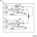
- FIG 8 illustrates schematically an example radar transceiver 800 comprising a master transceiver 801 and a slave transceiver 802.
- Each transceiver 801, 802 comprises a clock signal generator 805a, 805b.
- the phase relationship between the clock signals output by the clock signal generators 805a, 805b is set by phase select input signals 806a, 806b.
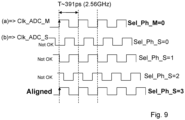
- Figure 9 illustrates the phase relationship between the master and slave clock signals Clk_ADC_M, Clk_ADC_S with varying phase select signals Sel_Ph_M, Sel_Ph_S. With the slave phase select signal set to 3 the clock signals are aligned.
- the example shown in Figure 9 illustrates clock signals at 2.56 GHz, i.e.
- Each clock signal generator 805a, 805b may be in the form of a clock signal generator as described above.
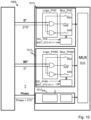
- FIG 10 illustrates an example circuit 1000 in which a multi-phase clock signal generator 1012, such as a divider, provides a clock signal with multiple phases to a plurality of duty cycle generators 1013 1-N .
- a multi-phase clock signal generator 1012 such as a divider
- Each duty cycle generator 1013 1-N is of the form as described above in relation to Figure 4 , except that the first AND gate 401 of the logic module 302 of Figure 4 is not provided.
- the outputs from each duty cycle generator are provided to a common multiplexer 1010.
- the circuit 1000 enables a calibrated initial phase relationship to be maintained while allowing a self-test to check operation of the duty cycle detectors. In each case, to allow for selection of a high (e.g. 75%), low (e.g. 25%) and normal (e.g.
- the inputs for each duty cycle generator 1013 1-N comprise a first clock signal at a first phase and a second clock signal at a second phase, where the second phase is shifted from the first phase by 270°.
- Tables 1 and 2 below show the inputs for each duty cycle generator and the corresponding output duty cycle values.
- the DTC values in each case are in relation to a local reference phase, which may differ in the case of a master and slave configuration. Depending on the phase selected at the slave side to allow for alignment with the master device, as described above, the phase may be different to that of the master device.
- the phase value input to duty cycle generator 1013 N may therefore be different to the phases input to the other generators 1013 1,2 .
- Table 1 Phase selection and switch values for duty cycle generator 1013 1 .
- Sel_PH0 1 Normal 0 0 closed open open ⁇ 50%
- Sel_PH0 1 BIST_dtcL 1 0 open closed open ⁇ 25%
- Sel_PH0 1 BIST_dtcH 0 1 open open closed ⁇ 75%
- Table 2 Phase selection and switch values for duty cycle generator 1013 2 .
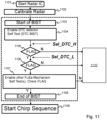
- FIG 11 illustrates an example flowchart showing a method of operating a radar transceiver during start-up, involving a self-test procedure to check operation of duty cycle detectors.
- the radar IC is started at step 1101, following which at step 1102 the radar is calibrated, for example by adjusting clock signal phases until master and slave transceivers are in phase.
- a BIST procedure is then started (step 1103), beginning with enabling a DTC detector self-test (step 1104).
- a first select signal Sel_DTC_H is input to the duty cycle generator of the clock signal generator to select a duty cycle above the normal duty cycle of 50%, for example at 75%.
- a check is done (step 1105) to determine whether the duty cycle detector outputs a flag.
- a second select signal Sel_DTC_L to select a duty cycle below the normal duty cycle, for example 25%, and another check is carried out (step 1106). If a flag is output, other self-tests may be carried out (step 1107), following which the BIST routine ends (step 1108) and a chirp sequence begins (step 1109). If, at any of steps 1105, 1106 or 1107 an output flag is not detected, an alert is provided 1110 indicating a safety mechanism is corrupted.
- An additional phase calibration step may be provided as part of step 1104 to ensure that master and slave transceivers of a radar transceiver are in a correct phase aligned relationship.
Landscapes
- Engineering & Computer Science (AREA)
- Physics & Mathematics (AREA)
- General Physics & Mathematics (AREA)
- Radar, Positioning & Navigation (AREA)
- Remote Sensing (AREA)
- Computer Networks & Wireless Communication (AREA)
- General Engineering & Computer Science (AREA)
- Nonlinear Science (AREA)
- Stabilization Of Oscillater, Synchronisation, Frequency Synthesizers (AREA)
- Manipulation Of Pulses (AREA)
Claims (14)
- Circuit (201, 501) comprenant :un générateur de signal d'horloge (205, 505) configuré pour fournir un signal d'horloge de sortie (203) ayant un certain rapport cyclique ;un détecteur de rapport cyclique (208) conçu pour recevoir le signal d'horloge de sortie (203) et fournir un indicateur de sortie si le rapport cyclique du signal d'horloge de sortie (203) est en dehors d'une plage prédéterminée entre 45 % et 55 % ;un contrôleur (214) conçu pour fournir un signal de sélection de rapport cyclique (216) au générateur de signal d'horloge (205, 505) afin que le signal d'horloge de sortie (203) ait un rapport cyclique en dehors de la plage prédéterminée et pour recevoir l'indicateur de sortie afin de confirmer le fonctionnement du détecteur de rapport cyclique (208).
- Circuit (201, 501) selon la revendication 1,
dans lequel le contrôleur (214) est configuré, dans un premier mode, pour fournir un premier signal de sélection de rapport cyclique (216) pour amener le générateur de signal d'horloge (205, 505) à fournir le signal d'horloge de sortie (203) avec un premier rapport cyclique dans la plage prédéterminée et, dans un second mode, pour fournir un second signal de sélection de rapport cyclique (216) pour amener le générateur de signal d'horloge (205, 505) à fournir le signal d'horloge de sortie (203) avec un second rapport cyclique à l'extérieur de la plage prédéterminée. - Circuit (201, 501) selon la revendication 1 ou la revendication 2, dans lequel le générateur de signal d'horloge (205, 505) comprend un diviseur de signal d'horloge (212) et un générateur de rapport cyclique (213) conçu pour recevoir une pluralité de phases de signal d'horloge du diviseur de signal d'horloge (212) et émettre le signal d'horloge de sortie (203) ayant un rapport cyclique déterminé par le signal de sélection de rapport cyclique (216).
- Circuit (201, 501) selon la revendication 3, dans lequel le générateur de rapport cyclique (213) comprend un module logique (302) et un multiplexeur (303), le module logique étant conçu pour combiner la pluralité de phases de signaux d'horloge et émettre une pluralité de signaux d'horloge avec des rapports cycliques différents vers le multiplexeur (303), le multiplexeur sélectionnant le signal d'horloge de sortie (203) en fonction du signal de sélection de rapport cyclique (216).
- Circuit (201, 501) selon la revendication 4, dans lequel le module logique (302) comprend :
une première porte ET (401) conçue pour recevoir l'une de la pluralité de phases de signaux d'horloge et un 1 logique et pour émettre un premier signal d'horloge (DTC_nom) ayant un rapport cyclique dans la plage prédéterminée. - Circuit (201, 501) selon la revendication 4 ou la revendication 5, dans lequel le module logique (302) comprend :une deuxième porte ET (402) conçue pour recevoir une paire de la pluralité de phases de signaux d'horloge et émettre un deuxième signal d'horloge (DTC_high) dont le rapport cyclique se situe en dehors de la plage prédéterminée ; et/ouune troisième porte ET (403) conçue pour recevoir la paire de la pluralité de phases de signaux d'horloge et ayant une sortie inversée pour émettre un troisième signal d'horloge (DTC_low) ayant un rapport cyclique en dehors de la plage prédéterminée.
- Circuit (201, 501) selon l'une quelconque des revendications 3 à 6, dans lequel la pluralité de phases de signaux d'horloge comprennent un premier signal d'horloge à une première phase et un deuxième signal d'horloge à une deuxième phase, la deuxième phase étant décalée de 270° par rapport à la première phase.
- Circuit (201, 501) selon l'une quelconque des revendications précédentes, dans lequel le générateur de signal d'horloge (205, 505) comprend une pluralité de générateurs de rapport cyclique (5131-N) chacun agencé pour recevoir une pluralité de phases de signaux d'horloge à partir d'un diviseur de signal d'horloge respectif (5121-N) et émettre un signal d'horloge (5031-N) dépendant d'un signal de sélection de rapport cyclique (5161-N) reçu du contrôleur (514).
- Émetteur-récepteur radar (800) comprenant un circuit (201, 501) selon l'une quelconque des revendications précédentes.
- Émetteur-récepteur radar (800) selon la revendication 9, comprenant un émetteur-récepteur maître et un émetteur-récepteur esclave (801, 802) comprenant chacun un circuit respectif (201, 501) selon l'une quelconque des revendications 1 à 8, dans lequel la phase d'un signal d'horloge émis par chaque générateur de signal d'horloge (805a, 805b), de chaque circuit respectif (201, 501), est réglable en fonction d'un signal d'entrée de sélection de phase (806a, 806b).
- Procédé de test d'un détecteur de rapport cyclique (208) connecté à un générateur de signal d'horloge (205), dans lequel le détecteur de rapport cyclique (208) et le générateur de signal d'horloge (205, 505) sont compris dans un circuit (201, 501) selon l'une quelconque des revendications 1 à 8, le procédé comprenant les étapes suivantes :i) fournir un signal de sélection de rapport cyclique (216) au générateur de signal d'horloge (205, 505) pour que le signal d'horloge (203) ait un rapport cyclique en dehors de la plage prédéterminée ; etii) détecter un indicateur de sortie du détecteur de rapport cyclique (208) pour confirmer le fonctionnement du détecteur de rapport cyclique (208).
- Procédé selon la revendication 11, dans lequel l'étape i) comprend les étapes suivantes :ia) fournir un premier signal de sélection de rapport cyclique (Sel_DTC_H) au générateur de signal d'horloge pour que le signal d'horloge (203) ait un rapport cyclique supérieur à la plage prédéterminée ; etib) fournir un deuxième signal de sélection de rapport cyclique (Sel_DTC_L) au générateur de signal d'horloge pour que le signal d'horloge (203) ait un rapport cyclique inférieur à la plage prédéterminée,dans lequel l'étape ii) comprend de détecter l'indicateur de sortie du détecteur de rapport cyclique (208) après les deux étapes ia) et ib) pour confirmer le fonctionnement du détecteur de rapport cyclique (208).
- Procédé selon la revendication 11 ou la revendication 12, dans lequel le circuit (201, 501) comprend un émetteur-récepteur radar (800).
- Procédé selon la revendication 13, dans lequel l'émetteur-récepteur radar comprend un émetteur-récepteur maître et un émetteur-récepteur esclave (801, 802) comprenant chacun un circuit respectif (201, 501) selon l'une quelconque des revendications 1 à 8, le procédé comprenant d'aligner la phase d'un signal d'horloge de l'émetteur-récepteur esclave et de l'émetteur-récepteur maître pour fournir un signal d'horloge de phase aligné pour le générateur de rapport cyclique de chaque circuit respectif (201, 501).
Priority Applications (3)
| Application Number | Priority Date | Filing Date | Title |
|---|---|---|---|
| EP20305638.7A EP3923005B1 (fr) | 2020-06-11 | 2020-06-11 | Auto-test d'un détecteur de cycle de service |
| US17/336,843 US11815553B2 (en) | 2020-06-11 | 2021-06-02 | Duty cycle detector self-testing |
| CN202110634817.4A CN113810027A (zh) | 2020-06-11 | 2021-06-08 | 占空比检测器自测 |
Applications Claiming Priority (1)
| Application Number | Priority Date | Filing Date | Title |
|---|---|---|---|
| EP20305638.7A EP3923005B1 (fr) | 2020-06-11 | 2020-06-11 | Auto-test d'un détecteur de cycle de service |
Publications (2)
| Publication Number | Publication Date |
|---|---|
| EP3923005A1 EP3923005A1 (fr) | 2021-12-15 |
| EP3923005B1 true EP3923005B1 (fr) | 2024-08-07 |
Family
ID=71575284
Family Applications (1)
| Application Number | Title | Priority Date | Filing Date |
|---|---|---|---|
| EP20305638.7A Active EP3923005B1 (fr) | 2020-06-11 | 2020-06-11 | Auto-test d'un détecteur de cycle de service |
Country Status (3)
| Country | Link |
|---|---|
| US (1) | US11815553B2 (fr) |
| EP (1) | EP3923005B1 (fr) |
| CN (1) | CN113810027A (fr) |
Families Citing this family (2)
| Publication number | Priority date | Publication date | Assignee | Title |
|---|---|---|---|---|
| CN115001423A (zh) * | 2022-05-16 | 2022-09-02 | 上海交通大学 | 一种用于多种生理电信号采集的感知放大电路 |
| CN119380790B (zh) * | 2023-07-20 | 2025-10-21 | 珠海横琴芯存半导体有限公司 | 随机存储器及测试装置 |
Family Cites Families (17)
| Publication number | Priority date | Publication date | Assignee | Title |
|---|---|---|---|---|
| KR100366626B1 (ko) * | 2000-08-14 | 2003-01-09 | 삼성전자 주식회사 | 부정합에 둔감한 듀티사이클 검출회로 |
| US7062692B1 (en) * | 2002-09-26 | 2006-06-13 | Xilinx, Inc. | Duty cycle characterization and adjustment |
| EP1475907B1 (fr) * | 2003-05-05 | 2005-09-07 | Harman Becker Automotive Systems GmbH | Méthode de test d'un convertisseur optique-electrique |
| US7961559B2 (en) | 2003-11-13 | 2011-06-14 | International Business Machines Corporation | Duty cycle measurement circuit for measuring and maintaining balanced clock duty cycle |
| TW200719617A (en) | 2005-07-15 | 2007-05-16 | Koninkl Philips Electronics Nv | Testing method and apparatus for a transmission and reception system |
| US20070075753A1 (en) | 2005-09-30 | 2007-04-05 | Rachael Parker | Duty cycle measurement circuit |
| WO2010018544A1 (fr) * | 2008-08-12 | 2010-02-18 | Nxp B.V. | Test d’un système de réception et de transmission |
| US8344925B1 (en) * | 2011-05-26 | 2013-01-01 | Cadence Design Systems, Inc. | System and method for adaptive timing control of successive approximation analog-to-digital conversion |
| US8736329B1 (en) * | 2013-02-06 | 2014-05-27 | Qualcomm Incorporated | Systems and methods for providing duty cycle correction |
| US8773186B1 (en) | 2013-08-01 | 2014-07-08 | Elite Semiconductor Memory Technology Inc. | Duty cycle correction circuit |
| US9030244B1 (en) | 2014-01-15 | 2015-05-12 | Altera Corporation | Clock duty cycle calibration circuitry |
| US9805773B1 (en) | 2016-05-23 | 2017-10-31 | Intel Corporation | Dual-range clock duty cycle corrector |
| DE102019121891A1 (de) * | 2018-08-20 | 2020-02-20 | Taiwan Semiconductor Manufacturing Company, Ltd. | Takt-arbeitszyklus-einstell- und kalibrieschaltung und verfahren zum betreiben derselben |
| US10890938B2 (en) * | 2018-08-20 | 2021-01-12 | Taiwan Semiconductor Manufacturing Company Ltd. | Clock duty cycle adjustment and calibration circuit and method of operating same |
| EP3648348B1 (fr) | 2018-10-29 | 2022-09-28 | NXP USA, Inc. | Circuit de surveillance de cycle de travail et procédé de surveillance de cycle de service |
| US10601410B1 (en) * | 2018-11-02 | 2020-03-24 | Micron Technology, Inc. | Offset cancellation of duty cycle detector |
| US10892742B2 (en) * | 2019-01-07 | 2021-01-12 | Texas Instruments Incorporated | Duty-cycle calibration based on differential clock sensing |
-
2020
- 2020-06-11 EP EP20305638.7A patent/EP3923005B1/fr active Active
-
2021
- 2021-06-02 US US17/336,843 patent/US11815553B2/en active Active
- 2021-06-08 CN CN202110634817.4A patent/CN113810027A/zh active Pending
Also Published As
| Publication number | Publication date |
|---|---|
| CN113810027A (zh) | 2021-12-17 |
| EP3923005A1 (fr) | 2021-12-15 |
| US20210389372A1 (en) | 2021-12-16 |
| US11815553B2 (en) | 2023-11-14 |
Similar Documents
| Publication | Publication Date | Title |
|---|---|---|
| US6859028B2 (en) | Design-for-test modes for a phase locked loop | |
| US6421801B1 (en) | Testing IO timing in a delay locked system using separate transmit and receive loops | |
| US9897975B2 (en) | Calibration method and apparatus for high TDC resolution | |
| US20080001642A1 (en) | Delay-locked loop apparatus adjusting internal clock signal in synchronization with external clock signal | |
| US7688123B2 (en) | Delay apparatus, and delay locked loop circuit and semiconductor memory apparatus using the same | |
| CN111064465B (zh) | 频率漂移检测器、通信单元和其方法 | |
| US7330502B2 (en) | Input/output circuit and semiconductor integrated circuit | |
| US11815553B2 (en) | Duty cycle detector self-testing | |
| JP3892847B2 (ja) | 半導体集積回路及び半導体集積回路のテスト方法 | |
| US8291257B2 (en) | Apparatus and method to compensate for injection locking | |
| US20110169501A1 (en) | Delay circuit | |
| US7023195B2 (en) | Module, system and method for testing a phase locked loop | |
| US20140218060A1 (en) | Degradation diagnosing circuit and degradation diagnosing method | |
| US6998889B2 (en) | Circuit, apparatus and method for obtaining a lock state value | |
| US7298790B2 (en) | Low frequency self-calibration of a PLL with multiphase clocks | |
| US6476594B1 (en) | Method and apparatus for testing high frequency delay locked loops | |
| US20090271133A1 (en) | Clock jitter measurement circuit and integrated circuit having the same | |
| US20060109059A1 (en) | System and method for maintaining an accurate frequency on a voltage controlled oscillator | |
| US6470483B1 (en) | Method and apparatus for measuring internal clock skew | |
| US7519844B2 (en) | PVT drift compensation | |
| US7613237B1 (en) | Built-in test feature to facilitate system level stress testing of a high-speed serial link that uses a forwarding clock | |
| JP2004274527A (ja) | データ送受信装置 | |
| US7555094B2 (en) | Counter capable of holding and outputting a count value and phase locked loop having the counter | |
| US20040128603A1 (en) | Device for testing the conformity of an electronic connection | |
| US6373313B1 (en) | Delay time regulation method and delay time regulation circuit |
Legal Events
| Date | Code | Title | Description |
|---|---|---|---|
| PUAI | Public reference made under article 153(3) epc to a published international application that has entered the european phase |
Free format text: ORIGINAL CODE: 0009012 |
|
| STAA | Information on the status of an ep patent application or granted ep patent |
Free format text: STATUS: THE APPLICATION HAS BEEN PUBLISHED |
|
| AK | Designated contracting states |
Kind code of ref document: A1 Designated state(s): AL AT BE BG CH CY CZ DE DK EE ES FI FR GB GR HR HU IE IS IT LI LT LU LV MC MK MT NL NO PL PT RO RS SE SI SK SM TR |
|
| B565 | Issuance of search results under rule 164(2) epc |
Effective date: 20201204 |
|
| STAA | Information on the status of an ep patent application or granted ep patent |
Free format text: STATUS: REQUEST FOR EXAMINATION WAS MADE |
|
| 17P | Request for examination filed |
Effective date: 20220615 |
|
| RBV | Designated contracting states (corrected) |
Designated state(s): AL AT BE BG CH CY CZ DE DK EE ES FI FR GB GR HR HU IE IS IT LI LT LU LV MC MK MT NL NO PL PT RO RS SE SI SK SM TR |
|
| GRAP | Despatch of communication of intention to grant a patent |
Free format text: ORIGINAL CODE: EPIDOSNIGR1 |
|
| STAA | Information on the status of an ep patent application or granted ep patent |
Free format text: STATUS: GRANT OF PATENT IS INTENDED |
|
| RIC1 | Information provided on ipc code assigned before grant |
Ipc: G01R 29/02 20060101ALI20240209BHEP Ipc: G01R 31/317 20060101AFI20240209BHEP |
|
| INTG | Intention to grant announced |
Effective date: 20240320 |
|
| GRAS | Grant fee paid |
Free format text: ORIGINAL CODE: EPIDOSNIGR3 |
|
| GRAA | (expected) grant |
Free format text: ORIGINAL CODE: 0009210 |
|
| STAA | Information on the status of an ep patent application or granted ep patent |
Free format text: STATUS: THE PATENT HAS BEEN GRANTED |
|
| AK | Designated contracting states |
Kind code of ref document: B1 Designated state(s): AL AT BE BG CH CY CZ DE DK EE ES FI FR GB GR HR HU IE IS IT LI LT LU LV MC MK MT NL NO PL PT RO RS SE SI SK SM TR |
|
| REG | Reference to a national code |
Ref country code: GB Ref legal event code: FG4D |
|
| REG | Reference to a national code |
Ref country code: CH Ref legal event code: EP |
|
| REG | Reference to a national code |
Ref country code: IE Ref legal event code: FG4D |
|
| REG | Reference to a national code |
Ref country code: DE Ref legal event code: R096 Ref document number: 602020035248 Country of ref document: DE |
|
| REG | Reference to a national code |
Ref country code: LT Ref legal event code: MG9D |
|
| REG | Reference to a national code |
Ref country code: NL Ref legal event code: MP Effective date: 20240807 |
|
| PG25 | Lapsed in a contracting state [announced via postgrant information from national office to epo] |
Ref country code: NO Free format text: LAPSE BECAUSE OF FAILURE TO SUBMIT A TRANSLATION OF THE DESCRIPTION OR TO PAY THE FEE WITHIN THE PRESCRIBED TIME-LIMIT Effective date: 20241107 |
|
| REG | Reference to a national code |
Ref country code: AT Ref legal event code: MK05 Ref document number: 1711516 Country of ref document: AT Kind code of ref document: T Effective date: 20240807 |
|
| PG25 | Lapsed in a contracting state [announced via postgrant information from national office to epo] |
Ref country code: NL Free format text: LAPSE BECAUSE OF FAILURE TO SUBMIT A TRANSLATION OF THE DESCRIPTION OR TO PAY THE FEE WITHIN THE PRESCRIBED TIME-LIMIT Effective date: 20240807 Ref country code: FI Free format text: LAPSE BECAUSE OF FAILURE TO SUBMIT A TRANSLATION OF THE DESCRIPTION OR TO PAY THE FEE WITHIN THE PRESCRIBED TIME-LIMIT Effective date: 20240807 Ref country code: PT Free format text: LAPSE BECAUSE OF FAILURE TO SUBMIT A TRANSLATION OF THE DESCRIPTION OR TO PAY THE FEE WITHIN THE PRESCRIBED TIME-LIMIT Effective date: 20241209 Ref country code: PL Free format text: LAPSE BECAUSE OF FAILURE TO SUBMIT A TRANSLATION OF THE DESCRIPTION OR TO PAY THE FEE WITHIN THE PRESCRIBED TIME-LIMIT Effective date: 20240807 Ref country code: GR Free format text: LAPSE BECAUSE OF FAILURE TO SUBMIT A TRANSLATION OF THE DESCRIPTION OR TO PAY THE FEE WITHIN THE PRESCRIBED TIME-LIMIT Effective date: 20241108 |
|
| PG25 | Lapsed in a contracting state [announced via postgrant information from national office to epo] |
Ref country code: BG Free format text: LAPSE BECAUSE OF FAILURE TO SUBMIT A TRANSLATION OF THE DESCRIPTION OR TO PAY THE FEE WITHIN THE PRESCRIBED TIME-LIMIT Effective date: 20240807 |
|
| PG25 | Lapsed in a contracting state [announced via postgrant information from national office to epo] |
Ref country code: LV Free format text: LAPSE BECAUSE OF FAILURE TO SUBMIT A TRANSLATION OF THE DESCRIPTION OR TO PAY THE FEE WITHIN THE PRESCRIBED TIME-LIMIT Effective date: 20240807 |
|
| PG25 | Lapsed in a contracting state [announced via postgrant information from national office to epo] |
Ref country code: AT Free format text: LAPSE BECAUSE OF FAILURE TO SUBMIT A TRANSLATION OF THE DESCRIPTION OR TO PAY THE FEE WITHIN THE PRESCRIBED TIME-LIMIT Effective date: 20240807 Ref country code: IS Free format text: LAPSE BECAUSE OF FAILURE TO SUBMIT A TRANSLATION OF THE DESCRIPTION OR TO PAY THE FEE WITHIN THE PRESCRIBED TIME-LIMIT Effective date: 20241207 |
|
| PG25 | Lapsed in a contracting state [announced via postgrant information from national office to epo] |
Ref country code: HR Free format text: LAPSE BECAUSE OF FAILURE TO SUBMIT A TRANSLATION OF THE DESCRIPTION OR TO PAY THE FEE WITHIN THE PRESCRIBED TIME-LIMIT Effective date: 20240807 |
|
| PG25 | Lapsed in a contracting state [announced via postgrant information from national office to epo] |
Ref country code: ES Free format text: LAPSE BECAUSE OF FAILURE TO SUBMIT A TRANSLATION OF THE DESCRIPTION OR TO PAY THE FEE WITHIN THE PRESCRIBED TIME-LIMIT Effective date: 20240807 Ref country code: RS Free format text: LAPSE BECAUSE OF FAILURE TO SUBMIT A TRANSLATION OF THE DESCRIPTION OR TO PAY THE FEE WITHIN THE PRESCRIBED TIME-LIMIT Effective date: 20241107 |
|
| PG25 | Lapsed in a contracting state [announced via postgrant information from national office to epo] |
Ref country code: RS Free format text: LAPSE BECAUSE OF FAILURE TO SUBMIT A TRANSLATION OF THE DESCRIPTION OR TO PAY THE FEE WITHIN THE PRESCRIBED TIME-LIMIT Effective date: 20241107 Ref country code: PT Free format text: LAPSE BECAUSE OF FAILURE TO SUBMIT A TRANSLATION OF THE DESCRIPTION OR TO PAY THE FEE WITHIN THE PRESCRIBED TIME-LIMIT Effective date: 20241209 Ref country code: PL Free format text: LAPSE BECAUSE OF FAILURE TO SUBMIT A TRANSLATION OF THE DESCRIPTION OR TO PAY THE FEE WITHIN THE PRESCRIBED TIME-LIMIT Effective date: 20240807 Ref country code: NO Free format text: LAPSE BECAUSE OF FAILURE TO SUBMIT A TRANSLATION OF THE DESCRIPTION OR TO PAY THE FEE WITHIN THE PRESCRIBED TIME-LIMIT Effective date: 20241107 Ref country code: NL Free format text: LAPSE BECAUSE OF FAILURE TO SUBMIT A TRANSLATION OF THE DESCRIPTION OR TO PAY THE FEE WITHIN THE PRESCRIBED TIME-LIMIT Effective date: 20240807 Ref country code: LV Free format text: LAPSE BECAUSE OF FAILURE TO SUBMIT A TRANSLATION OF THE DESCRIPTION OR TO PAY THE FEE WITHIN THE PRESCRIBED TIME-LIMIT Effective date: 20240807 Ref country code: IS Free format text: LAPSE BECAUSE OF FAILURE TO SUBMIT A TRANSLATION OF THE DESCRIPTION OR TO PAY THE FEE WITHIN THE PRESCRIBED TIME-LIMIT Effective date: 20241207 Ref country code: HR Free format text: LAPSE BECAUSE OF FAILURE TO SUBMIT A TRANSLATION OF THE DESCRIPTION OR TO PAY THE FEE WITHIN THE PRESCRIBED TIME-LIMIT Effective date: 20240807 Ref country code: GR Free format text: LAPSE BECAUSE OF FAILURE TO SUBMIT A TRANSLATION OF THE DESCRIPTION OR TO PAY THE FEE WITHIN THE PRESCRIBED TIME-LIMIT Effective date: 20241108 Ref country code: FI Free format text: LAPSE BECAUSE OF FAILURE TO SUBMIT A TRANSLATION OF THE DESCRIPTION OR TO PAY THE FEE WITHIN THE PRESCRIBED TIME-LIMIT Effective date: 20240807 Ref country code: ES Free format text: LAPSE BECAUSE OF FAILURE TO SUBMIT A TRANSLATION OF THE DESCRIPTION OR TO PAY THE FEE WITHIN THE PRESCRIBED TIME-LIMIT Effective date: 20240807 Ref country code: BG Free format text: LAPSE BECAUSE OF FAILURE TO SUBMIT A TRANSLATION OF THE DESCRIPTION OR TO PAY THE FEE WITHIN THE PRESCRIBED TIME-LIMIT Effective date: 20240807 Ref country code: AT Free format text: LAPSE BECAUSE OF FAILURE TO SUBMIT A TRANSLATION OF THE DESCRIPTION OR TO PAY THE FEE WITHIN THE PRESCRIBED TIME-LIMIT Effective date: 20240807 |
|
| PG25 | Lapsed in a contracting state [announced via postgrant information from national office to epo] |
Ref country code: DK Free format text: LAPSE BECAUSE OF FAILURE TO SUBMIT A TRANSLATION OF THE DESCRIPTION OR TO PAY THE FEE WITHIN THE PRESCRIBED TIME-LIMIT Effective date: 20240807 Ref country code: SM Free format text: LAPSE BECAUSE OF FAILURE TO SUBMIT A TRANSLATION OF THE DESCRIPTION OR TO PAY THE FEE WITHIN THE PRESCRIBED TIME-LIMIT Effective date: 20240807 |
|
| PG25 | Lapsed in a contracting state [announced via postgrant information from national office to epo] |
Ref country code: EE Free format text: LAPSE BECAUSE OF FAILURE TO SUBMIT A TRANSLATION OF THE DESCRIPTION OR TO PAY THE FEE WITHIN THE PRESCRIBED TIME-LIMIT Effective date: 20240807 |
|
| PG25 | Lapsed in a contracting state [announced via postgrant information from national office to epo] |
Ref country code: CZ Free format text: LAPSE BECAUSE OF FAILURE TO SUBMIT A TRANSLATION OF THE DESCRIPTION OR TO PAY THE FEE WITHIN THE PRESCRIBED TIME-LIMIT Effective date: 20240807 |
|
| PG25 | Lapsed in a contracting state [announced via postgrant information from national office to epo] |
Ref country code: SK Free format text: LAPSE BECAUSE OF FAILURE TO SUBMIT A TRANSLATION OF THE DESCRIPTION OR TO PAY THE FEE WITHIN THE PRESCRIBED TIME-LIMIT Effective date: 20240807 |
|
| REG | Reference to a national code |
Ref country code: DE Ref legal event code: R097 Ref document number: 602020035248 Country of ref document: DE |
|
| PLBE | No opposition filed within time limit |
Free format text: ORIGINAL CODE: 0009261 |
|
| STAA | Information on the status of an ep patent application or granted ep patent |
Free format text: STATUS: NO OPPOSITION FILED WITHIN TIME LIMIT |
|
| PGFP | Annual fee paid to national office [announced via postgrant information from national office to epo] |
Ref country code: DE Payment date: 20250520 Year of fee payment: 6 |
|
| 26N | No opposition filed |
Effective date: 20250508 |
|
| PGFP | Annual fee paid to national office [announced via postgrant information from national office to epo] |
Ref country code: FR Payment date: 20250520 Year of fee payment: 6 |
|
| P01 | Opt-out of the competence of the unified patent court (upc) registered |
Free format text: CASE NUMBER: APP_29918/2025 Effective date: 20250623 |
|
| PG25 | Lapsed in a contracting state [announced via postgrant information from national office to epo] |
Ref country code: SE Free format text: LAPSE BECAUSE OF FAILURE TO SUBMIT A TRANSLATION OF THE DESCRIPTION OR TO PAY THE FEE WITHIN THE PRESCRIBED TIME-LIMIT Effective date: 20240807 |
|
| REG | Reference to a national code |
Ref country code: CH Ref legal event code: H13 Free format text: ST27 STATUS EVENT CODE: U-0-0-H10-H13 (AS PROVIDED BY THE NATIONAL OFFICE) Effective date: 20260127 |
|
| PG25 | Lapsed in a contracting state [announced via postgrant information from national office to epo] |
Ref country code: IT Free format text: LAPSE BECAUSE OF FAILURE TO SUBMIT A TRANSLATION OF THE DESCRIPTION OR TO PAY THE FEE WITHIN THE PRESCRIBED TIME-LIMIT Effective date: 20240807 |
|
| PG25 | Lapsed in a contracting state [announced via postgrant information from national office to epo] |
Ref country code: MC Free format text: LAPSE BECAUSE OF FAILURE TO SUBMIT A TRANSLATION OF THE DESCRIPTION OR TO PAY THE FEE WITHIN THE PRESCRIBED TIME-LIMIT Effective date: 20240807 |
|
| PG25 | Lapsed in a contracting state [announced via postgrant information from national office to epo] |
Ref country code: LU Free format text: LAPSE BECAUSE OF NON-PAYMENT OF DUE FEES Effective date: 20250611 |
|
| GBPC | Gb: european patent ceased through non-payment of renewal fee |
Effective date: 20250611 |
|
| REG | Reference to a national code |
Ref country code: BE Ref legal event code: MM Effective date: 20250630 |
|
| PG25 | Lapsed in a contracting state [announced via postgrant information from national office to epo] |
Ref country code: GB Free format text: LAPSE BECAUSE OF NON-PAYMENT OF DUE FEES Effective date: 20250611 |
|
| PG25 | Lapsed in a contracting state [announced via postgrant information from national office to epo] |
Ref country code: IE Free format text: LAPSE BECAUSE OF NON-PAYMENT OF DUE FEES Effective date: 20250611 |
|
| PG25 | Lapsed in a contracting state [announced via postgrant information from national office to epo] |
Ref country code: RO Free format text: LAPSE BECAUSE OF FAILURE TO SUBMIT A TRANSLATION OF THE DESCRIPTION OR TO PAY THE FEE WITHIN THE PRESCRIBED TIME-LIMIT Effective date: 20240807 Ref country code: BE Free format text: LAPSE BECAUSE OF NON-PAYMENT OF DUE FEES Effective date: 20250630 |
|
| PG25 | Lapsed in a contracting state [announced via postgrant information from national office to epo] |
Ref country code: CH Free format text: LAPSE BECAUSE OF NON-PAYMENT OF DUE FEES Effective date: 20250630 |