EP3926437A1 - Hochgenaue zener-basierte spannungsreferenzschaltung - Google Patents
Hochgenaue zener-basierte spannungsreferenzschaltung Download PDFInfo
- Publication number
- EP3926437A1 EP3926437A1 EP20305656.9A EP20305656A EP3926437A1 EP 3926437 A1 EP3926437 A1 EP 3926437A1 EP 20305656 A EP20305656 A EP 20305656A EP 3926437 A1 EP3926437 A1 EP 3926437A1
- Authority
- EP
- European Patent Office
- Prior art keywords
- voltage
- node
- bipolar transistor
- voltage reference
- current
- Prior art date
- Legal status (The legal status is an assumption and is not a legal conclusion. Google has not performed a legal analysis and makes no representation as to the accuracy of the status listed.)
- Granted
Links
Images


Classifications
-
- G—PHYSICS
- G05—CONTROLLING; REGULATING
- G05F—SYSTEMS FOR REGULATING ELECTRIC OR MAGNETIC VARIABLES
- G05F3/00—Non-retroactive systems for regulating electric variables by using an uncontrolled element, or an uncontrolled combination of elements, such element or such combination having self-regulating properties
- G05F3/02—Regulating voltage or current
- G05F3/08—Regulating voltage or current wherein the variable is DC
- G05F3/10—Regulating voltage or current wherein the variable is DC using uncontrolled devices with non-linear characteristics
- G05F3/16—Regulating voltage or current wherein the variable is DC using uncontrolled devices with non-linear characteristics being semiconductor devices
- G05F3/18—Regulating voltage or current wherein the variable is DC using uncontrolled devices with non-linear characteristics being semiconductor devices using Zener diodes
- G05F3/185—Regulating voltage or current wherein the variable is DC using uncontrolled devices with non-linear characteristics being semiconductor devices using Zener diodes and field-effect transistors
-
- G—PHYSICS
- G05—CONTROLLING; REGULATING
- G05F—SYSTEMS FOR REGULATING ELECTRIC OR MAGNETIC VARIABLES
- G05F1/00—Automatic systems in which deviations of an electric quantity from one or more predetermined values are detected at the output of the system and fed back to a device within the system to restore the detected quantity to its predetermined value or values, i.e. retroactive systems
- G05F1/10—Regulating voltage or current
- G05F1/46—Regulating voltage or current wherein the variable actually regulated by the final control device is DC
- G05F1/56—Regulating voltage or current wherein the variable actually regulated by the final control device is DC using semiconductor devices in series with the load as final control devices
- G05F1/565—Regulating voltage or current wherein the variable actually regulated by the final control device is DC using semiconductor devices in series with the load as final control devices sensing a condition of the system or its load in addition to means responsive to deviations in the output of the system, e.g. current, voltage, power factor
- G05F1/567—Regulating voltage or current wherein the variable actually regulated by the final control device is DC using semiconductor devices in series with the load as final control devices sensing a condition of the system or its load in addition to means responsive to deviations in the output of the system, e.g. current, voltage, power factor for temperature compensation
-
- G—PHYSICS
- G05—CONTROLLING; REGULATING
- G05F—SYSTEMS FOR REGULATING ELECTRIC OR MAGNETIC VARIABLES
- G05F3/00—Non-retroactive systems for regulating electric variables by using an uncontrolled element, or an uncontrolled combination of elements, such element or such combination having self-regulating properties
- G05F3/02—Regulating voltage or current
- G05F3/08—Regulating voltage or current wherein the variable is DC
- G05F3/10—Regulating voltage or current wherein the variable is DC using uncontrolled devices with non-linear characteristics
- G05F3/16—Regulating voltage or current wherein the variable is DC using uncontrolled devices with non-linear characteristics being semiconductor devices
- G05F3/20—Regulating voltage or current wherein the variable is DC using uncontrolled devices with non-linear characteristics being semiconductor devices using diode- transistor combinations
- G05F3/22—Regulating voltage or current wherein the variable is DC using uncontrolled devices with non-linear characteristics being semiconductor devices using diode- transistor combinations wherein the transistors are of the bipolar type only
Definitions
- the present disclosure relates to voltage reference circuits, and in particular to temperature compensated Zener based voltage reference circuits.
- BMS battery management system
- bandgap circuits are used to provide a known reference voltage.
- reference voltage circuits based on a Zener diode are an attractive alternative.
- the voltage across Zener a diode varies only slowly with the current through the diode, and thus the diode can form the basis of an accurate reference voltage.
- Zener diodes generally have a positive temperature coefficient (TC), that is to say for a fixed current, the voltage across the diode increases with increasing temperature, and thus temperature compensation is required by adding a circuit which is complementary to absolute temperature (CTAT)
- a voltage reference circuit comprising: a supply terminal configured to be connected to a supply voltage; a ground terminal configured to be connected to a ground voltage; a first current source and a Zener diode connected in series between the supply terminal and the ground terminal and having a first node therebetween and configured to supply a Zener voltage at the first node (Vz); an output node (Vref_hv) configured to provide a voltage reference (Vref_hv, Vref); and a complementary to absolute temperature, CTAT, circuit connected between the first node and the output node; wherein the CTAT circuit comprises: a first bipolar transistor (Q1) and a second bipolar transistor (Q2), each having a base, a collector and an emitter, having their respective emitters connected at a second node (Vs), and configured to, in operation, have equal collector-emitter currents, wherein the base of the first bipolar transistor is connected to the first node and the base of the second bipolar
- the CTAT circuit further comprises a second current source (I_BIAS_hs), connected between the collector of the first bipolar transistor and the supply node, and configured to provide a bias current to the first bipolar transistor.
- I_BIAS_hs second current source
- the CTAT circuit further comprises a FET having main terminals connected between the collector of the second bipolar transistor and the supply node, and a control terminal connected to the collector of the first bipolar transistor, and configured to match the collector-emitter currents through the first and second bipolar transistors.
- This arrangement may provide a particularly simple method of ensuring matched currents.
- the CTAT circuit further comprises a third current source, connected between the emitters of the first and second bipolar transistors, and the ground terminal.
- the third current source may be configured to sink a current equal to twice that supplied by the second current source plus a current through the second resistor. This may ensure precise matching of the emitter currents of the two bipolar transistors.
- current source is used herein to refer to both current sources, stricto senso, and current sinks.
- the voltage reference is provided directly at the output node.
- a second voltage divider comprising two resistors, or resistances, connected between the output node and ground and having a centre node therebetween, wherein the voltage reference (Vref) is at the centre node of the second voltage divider. This allows for scaling of the reference voltage to a particular chosen value or range.
- the first bipolar transistor and the second bipolar transistor are each NPN transistors.
- the first bipolar transistor and second bipolar transistor are matched transistors. That is to say, they may be designed to have the same or very similar characteristics. This may ensure that it is straightforward to apply a scaled version voltage from the base emitter voltage of Q2 to the Zener voltage Vz, despite there only being an indirect connection through Q1.
- the current through the second resistance is less than 100 nA. Using a low current through this voltage divider may ensure that the transistor currents are nearly identical.
- the voltage reference circuit is configured to operate with a supply voltage between 6 V and 7 V. This may not be possible in the prior art designs.
- the second current source and the third current source are each configured to have a zero temperature coefficient, 0TC.
- the third current source is configured to provide a current consisting of a proportional to absolute temperature, PTAT, component and a CTAT component, wherein the CTAT component is a scaled version of a current through the second resistor.
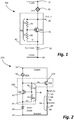
- Figure 1 illustrates a conventional voltage reference circuit 100 based on a Zener diode and including temperature compensation.
- Circuit 100 has a supply terminal 10 configured to receive a supply voltage, and a ground terminal 20 configured to operate at a ground voltage.
- the circuit includes a Zener diode 30, connected in series with a compensation circuit 40 and a current source 50 between the supply and ground.
- the current source 50 supplies a current IZEN through the Zener diode 30.
- the voltage Vz across the diode is relatively stable, but as already mentioned, exhibits a positive temperature coefficient.
- the compensation circuit 40 is therefore provided in series with the Zener diode to add a temperature dependent voltage to the Zener voltage Vz.
- the compensation for circuit 40 consists of a bipolar transistor Q1 42 connected in parallel with a voltage divider 44 consisting of lower resistor R2 46 and upper resistor R1 48.
- the base of the bipolar transistor is connected to the centre node of the resistive divisor, that is to say between R2 and R1, while the lower terminal of the voltage divider is connected to the emitter of the bipolar transistor at lower node 55 and the upper terminal of the voltage divider is connected to the collector of the bipolar transistor.
- the reference voltage Vref_hv at output node 60 is provided at the collector of the bipolar transistor.
- Vref_hv V Z + V be 1 + V R 1 where V R1 is the voltage across resistor R1, and V be1 is the emitter-base voltage of bipolar transistor Q1.
- Vref hv Vz + 1 + R 1 R 2 V be 1
- Vz has a positive temperature coefficient; however, this is compensated by the negative temperature coefficient of V be1 Since this negative temperature coefficient is approximately -2mV/°C, is it scaled by a factor (1 + R1/R2), where the ratio between R1 and R2 is chosen to cancel out the positive temperature coefficient of Zener diode. It will be appreciated the since (1+ R1/R2) is always greater than unity. So. when 0 mV/°C ⁇ TC1_zener ⁇ 2 mV/°C, this structure cannot, by itself, make a 0TC Vref_hv
- Figure 2 illustrates an alternative voltage reference circuit 200 based on a Zener diode and including temperature compensation.
- This circuit is generally similar to the circuit of figure 1 except that the compensation circuit relies on a V be of a second bipolar transistor which decouples the current through the bipolar transistor from the Zener current.
- Circuit 200 has a supply terminal 10 configured to receive a supply voltage, and a ground terminal 20 configured to operate at a ground voltage.
- the circuit includes a Zener diode 30, connected in series with a compensation circuit 240 and a current source IZEN 50 between the supply and ground.
- the current source 50 supplies a current through the Zener diode 30.
- the compensation circuit 40 is therefore provided in series with the Zener diode to add a temperature dependence voltage to the Zener voltage Vz.
- the compensation for circuit 240 consists of a bipolar transistor Q1 42 connected in parallel with a voltage divider 44 consisting of lower resistor R2 46 and upper resistor R1 48.
- the base of the bipolar transistor is connected to the centre node of the resistive divisor, that is to say between R2 and R1, while the lower terminal of the voltage divider is connected to the emitter of the bipolar transistor, at lower node 55, and the upper terminal of the voltage divider is connected to the collector of the bipolar transistor.
- This circuit differs from that shown in figure 1 in that the collector of Q1 at voltage Ve, is not directly connected as the reference voltage, but is connected to the base terminal of a second bipolar transistor Q2 270.
- This second bipolar transistor Q2 is connected in a second path between supply 10 and ground 20, in series with a second voltage divider 64 comprising two resistors R4 66 and R3 68 with a node Vref therebetween.
- V ref R 4 R 3 + R 4 .
- V Z + 1 + R 1 R 2 V be 1 ⁇ V be 2 where V be2 is the base emitter voltage of Q2.
- V be1 is equal to V be2
- V ref R 4 R 3 + R 4 .
- this circuit is similar to that of figure 1 , but instead of an invariant voltage reference Vref_hV, the value of the voltage reference, Vref, can be chosen by suitable choices of the resistors in the second resistive divisor 64.
- Figure 3 illustrates a voltage reference circuit 300 based on a Zener diode and including temperature compensation according to one or more embodiments.
- this circuit differs from the circuit shown in figures 1 and 2 in that the compensation circuit is not stacked on top of the diode, and can thus operate at a lower supply voltage.
- Circuit 300 has a supply terminal 10 configured to be connected to a supply voltage, and a ground terminal 20 configured to be connected to a ground voltage.
- the circuit includes a first current source 50 which supplies a current IZEN and a Zener diode 30 connected in series between the supply terminal and the ground terminal. Between the current source 50 and the Zener diode 30 is a first node 355 at which there is a Zener voltage (Vz).
- the Zener voltage node having voltage Vz is related to an output node 360, configured to provide a first voltage reference Vref_hv, by a compensation circuit.
- First voltage reference 360 may also be considered to be a high voltage reference as will become more apparent from the discussion of a lower voltage reference hereinbelow.
- the compensation circuit takes the form of a complementary to absolute temperature, CTAT, circuit 340 connected between the first node and the output node. That is to say, the voltage difference (between the Zener voltage Vz and the voltage Vref_hv at the output node) decreases as the temperature or absolute temperature increases.
- the CTAT circuit 240 comprises two bipolar transistors Q1 370 and Q2 380.
- the transistors are arranged to carry similar currents.
- the CTAT circuit is based on a first bipolar transistor Q1 370 and a second bipolar transistor Q2 380, each having a base, a collector and an emitter, having their respective emitters connected at a second node 365 at a voltage Vs, and configured to, in operation, have equal, or similar, collector-emitter currents.
- the base of the first bipolar transistor is connected to the first, Zener voltage, node and the base of the second bipolar transistor is connected to a centre node 305 of a voltage divider which consists of two resistances or resistors R1 315 and R2 325.
- the voltage divider is connected between the emitter of the second bipolar transistor and the output node (Vref_hv), that is to say it is connected in parallel with the second bipolar transistor Q2.
- a second current source 345 is connected between the collector of the first bipolar transistor and the supply node, and configured to provide a bias current I_BIAS_hs to the first bipolar transistor.
- a third current source 335 is connected between the common emitters of the first and second bipolar transistors and the ground terminal. This current source is configured to sink a current I-BIAS-Is from the pair of transistors.
- Transistors Q1 and Q2 are arranged in parallel in the sense that they each form part of two separate legs between the node 365 at voltage Vs (that is to say the high side of the first current source 335) and the voltage terminal 10.
- the two legs carry similar, or equal, current.
- the FET may be a p-channel mode FET.
- the FET is included in the same leg as the second bipolar transistor, and has its main terminals connected between the collector of the second bipolar transistor and the supply node, and a control terminal connected to the collector of the first bipolar transistor.
- the FET is configured to match the collector-emitter currents through the first and second legs - that is to say, through the first and second bipolar transistors.
- the current through the second leg is shared between the second bipolar transistor Q2 and the potential divider R1 R2.
- the current through the potential divider R1 R2 is chosen to be several orders of magnitude lower than the current through Q2, and is thus effectively negligible.
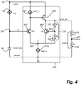
- FIG. 4 illustrates a voltage reference circuit based on a Zener diode and including temperature coefficient correction according to one or more other embodiments of the present disclosure.
- This circuit is broadly similar to the circuit of figure 3 : the directly corresponding parts do not need to be described in more detail.
- this circuit has an additional, second, voltage divider 410.
- This second voltage divider 410 comprises two resistors R3 415 and R4 425 connected between the output node 305 and ground.
- the second voltage divider has a centre node 405 between the resistors R1 and R2.
- the voltage reference 405, having voltage Vref, is at the centre node of the second voltage divider.
- this voltage divider operates to scale the high voltage output reference Vref_hv to the chosen reference voltage Vref.
- V R1 is the voltage across R1 in the first voltage divider.
- V ref R 4 R 3 + R 4 V Z + R 1 R 2 ⁇ V be 2
- the positive temperature coefficient of the Zener voltage, Vz is compensated by the negative temperature coefficient of the base-emitter voltage of Q2, V be2 .
- the temperature coefficient of V be2 is typically -2 mV/°C. Adjustment of the ratio R1 over R2 then allows for near-perfect cancellation of the positive voltage coefficient of the Zener diode.
- the supply voltage must be sufficient to provide the sum of the Zener voltage, the collector-emitter voltage of Q1, and the collector-base voltage of Q2.
- embodiments of the present disclosure as shown in figure 3 and 4 may operate with a lower supply voltage.
- the supply voltage is only required to supply provide sufficient headroom for the Zener voltage, the base-collector voltage of Q1, and any voltage drop required to provide the high-side current source IBIAS_hs 345.
- embodiments of the present disclosure may be configured to operate with a minimum supply voltage of approximately 6 V, in contrast to previous circuits such as that shown in figure 2 which generally require a minimum supply voltage of approximately 7 V.
- FIG. 5 this diagram illustrates a bias circuit 500 for providing bias currents to embodiments of the present disclosure, useing techniques familiar to the skilled person.
- the bias circuit provides a temperature compensated constant current, I OTC .
- the temperature compensated constant current I 0TC may be used, for example, as the current I_BIAS_hs in the high side current source 345.
- the temperature compensated constant current is provided as the sum of two currents, which are in turn determined using scaled current mirrors based on a complementary to absolute temperature (CTAT) current I CTAT and a proportional to absolute temperature (PTAT) current I PTAT respectively.
- CTAT complementary to absolute temperature
- PTAT proportional to absolute temperature
- the complementary to absolute temperature current is determined as the current through a resistor R5, 520, connected between the base and emitter of a first NPN bipolar transistor Q3 530.
- the first NPN bipolar transistor is connected, in series with a first FET M1 542, between a supply voltage 505 and a ground voltage 515.
- the current through R5 is supplied through a first leg M3 562 of a first scaled current mirror 560.
- the second leg M4 564 of the scaled current mirror provides this current, scaled by a factor ⁇ a:1>, as a first part of the current I 0TC .
- the proportional to absolute temperature current is determined as the current through a second resistor R6, 570, connected between the emitter of a second NPN bipolar transistor Q4 580 and ground.
- the collector of second NPN bipolar transistor is connected, in series with second FET M2 544 to the supply voltage 505.
- the second FET M2 544 is in a current mirror configuration 540 with first FET 542.
- This current mirror 540 includes a further, scaled, copy of the current through a further FET M5 546.
- This leg provides a copy of the current through R6, scaled by a factor of ⁇ b:1>, which is combined with the first scaled factor currents, to provide the second part of the current I 0TC .
- this temperature compensated current source I 0TC may be used directly to provide the current I_BIAS_hs to the high side current source.
- a similar circuit may be used to supply the current I_bias_Is to the low side bias current source 335.
- This current should be approximately twice the high side current.
- it should include the current IR2, which as mentioned above may be so low as to be negligible.
- IR2 C.ICTAT.
Landscapes
- Engineering & Computer Science (AREA)
- Physics & Mathematics (AREA)
- Electromagnetism (AREA)
- General Physics & Mathematics (AREA)
- Radar, Positioning & Navigation (AREA)
- Automation & Control Theory (AREA)
- Nonlinear Science (AREA)
- Microelectronics & Electronic Packaging (AREA)
- Control Of Electrical Variables (AREA)
Priority Applications (3)
| Application Number | Priority Date | Filing Date | Title |
|---|---|---|---|
| EP20305656.9A EP3926437B1 (de) | 2020-06-16 | 2020-06-16 | Hochgenaue zener-basierte spannungsreferenzschaltung |
| US17/322,175 US11480989B2 (en) | 2020-06-16 | 2021-05-17 | High accuracy zener based voltage reference circuit |
| CN202110649313.XA CN113805633B (zh) | 2020-06-16 | 2021-06-08 | 基于高准确度齐纳的电压参考电路 |
Applications Claiming Priority (1)
| Application Number | Priority Date | Filing Date | Title |
|---|---|---|---|
| EP20305656.9A EP3926437B1 (de) | 2020-06-16 | 2020-06-16 | Hochgenaue zener-basierte spannungsreferenzschaltung |
Publications (2)
| Publication Number | Publication Date |
|---|---|
| EP3926437A1 true EP3926437A1 (de) | 2021-12-22 |
| EP3926437B1 EP3926437B1 (de) | 2024-04-03 |
Family
ID=71575298
Family Applications (1)
| Application Number | Title | Priority Date | Filing Date |
|---|---|---|---|
| EP20305656.9A Active EP3926437B1 (de) | 2020-06-16 | 2020-06-16 | Hochgenaue zener-basierte spannungsreferenzschaltung |
Country Status (3)
| Country | Link |
|---|---|
| US (1) | US11480989B2 (de) |
| EP (1) | EP3926437B1 (de) |
| CN (1) | CN113805633B (de) |
Cited By (1)
| Publication number | Priority date | Publication date | Assignee | Title |
|---|---|---|---|---|
| US20210124386A1 (en) * | 2019-10-24 | 2021-04-29 | Nxp Usa, Inc. | Voltage reference generation with compensation for temperature variation |
Families Citing this family (4)
| Publication number | Priority date | Publication date | Assignee | Title |
|---|---|---|---|---|
| CN115903987B (zh) * | 2023-02-13 | 2025-03-25 | 北京士模微电子有限责任公司 | 一种新型Zener基准电路 |
| CN116069111B (zh) * | 2023-03-02 | 2025-09-19 | 南京微盟电子有限公司 | 一种高低温曲率补偿齐纳基准电压源电路 |
| US20250028343A1 (en) * | 2023-07-20 | 2025-01-23 | Texas Instruments Incorporated | In situ strain compensation afe |
| CN118012209B (zh) * | 2024-02-21 | 2026-04-07 | 中国电子科技集团公司第二十四研究所 | 一种带高阶温度补偿的低温漂隐埋齐纳基准电路 |
Citations (4)
| Publication number | Priority date | Publication date | Assignee | Title |
|---|---|---|---|---|
| US4560919A (en) * | 1983-11-30 | 1985-12-24 | Mitsubishi Denki Kabushiki Kaisha | Constant-voltage circuit insensitive to source change |
| US20150177771A1 (en) * | 2013-12-20 | 2015-06-25 | Analog Devices Technology | Low drift voltage reference |
| US20160197095A1 (en) * | 2013-09-11 | 2016-07-07 | Panasonic Intellectual Property Management Co., Ltd. | Semiconductor device |
| EP3553625A1 (de) * | 2018-04-13 | 2019-10-16 | NXP USA, Inc. | Zenerdioden-spannungsreferenzschaltung |
Family Cites Families (4)
| Publication number | Priority date | Publication date | Assignee | Title |
|---|---|---|---|---|
| JPS59195719A (ja) | 1983-04-20 | 1984-11-06 | Nec Corp | 基準電源 |
| FR2791193B1 (fr) * | 1999-03-16 | 2004-07-09 | St Microelectronics Sa | Procede de controle du fonctionnement d'une pompe de charge capacitive et dispositif de pompe de charge capacitive correspondant |
| JP4122910B2 (ja) * | 2002-09-24 | 2008-07-23 | ミツミ電機株式会社 | 電源供給回路 |
| EP3680745B1 (de) * | 2019-01-09 | 2022-12-21 | NXP USA, Inc. | Selbstvorgespannte temperaturkompensierte zener-referenz |
-
2020
- 2020-06-16 EP EP20305656.9A patent/EP3926437B1/de active Active
-
2021
- 2021-05-17 US US17/322,175 patent/US11480989B2/en active Active
- 2021-06-08 CN CN202110649313.XA patent/CN113805633B/zh active Active
Patent Citations (4)
| Publication number | Priority date | Publication date | Assignee | Title |
|---|---|---|---|---|
| US4560919A (en) * | 1983-11-30 | 1985-12-24 | Mitsubishi Denki Kabushiki Kaisha | Constant-voltage circuit insensitive to source change |
| US20160197095A1 (en) * | 2013-09-11 | 2016-07-07 | Panasonic Intellectual Property Management Co., Ltd. | Semiconductor device |
| US20150177771A1 (en) * | 2013-12-20 | 2015-06-25 | Analog Devices Technology | Low drift voltage reference |
| EP3553625A1 (de) * | 2018-04-13 | 2019-10-16 | NXP USA, Inc. | Zenerdioden-spannungsreferenzschaltung |
Cited By (2)
| Publication number | Priority date | Publication date | Assignee | Title |
|---|---|---|---|---|
| US20210124386A1 (en) * | 2019-10-24 | 2021-04-29 | Nxp Usa, Inc. | Voltage reference generation with compensation for temperature variation |
| US11774999B2 (en) * | 2019-10-24 | 2023-10-03 | Nxp Usa, Inc. | Voltage reference generation with compensation for temperature variation |
Also Published As
| Publication number | Publication date |
|---|---|
| US11480989B2 (en) | 2022-10-25 |
| EP3926437B1 (de) | 2024-04-03 |
| CN113805633A (zh) | 2021-12-17 |
| CN113805633B (zh) | 2025-09-16 |
| US20210389791A1 (en) | 2021-12-16 |
Similar Documents
| Publication | Publication Date | Title |
|---|---|---|
| EP3926437B1 (de) | Hochgenaue zener-basierte spannungsreferenzschaltung | |
| US7173407B2 (en) | Proportional to absolute temperature voltage circuit | |
| US4352056A (en) | Solid-state voltage reference providing a regulated voltage having a high magnitude | |
| US4249122A (en) | Temperature compensated bandgap IC voltage references | |
| US6828847B1 (en) | Bandgap voltage reference circuit and method for producing a temperature curvature corrected voltage reference | |
| US6956727B1 (en) | High side current monitor with extended voltage range | |
| US10788851B2 (en) | Self-biased temperature-compensated Zener reference | |
| US7012416B2 (en) | Bandgap voltage reference | |
| US6426669B1 (en) | Low voltage bandgap reference circuit | |
| US6172555B1 (en) | Bandgap voltage reference circuit | |
| US10712763B2 (en) | Sub-bandgap reference voltage source | |
| US20080116875A1 (en) | Systems, apparatus and methods relating to bandgap circuits | |
| EP3929694B1 (de) | Spannungsregler | |
| US4302718A (en) | Reference potential generating circuits | |
| US7170334B2 (en) | Switched current temperature sensing circuit and method to correct errors due to beta and series resistance | |
| US11846962B2 (en) | Bandgap reference circuit | |
| JP2001510609A (ja) | 温度補償された出力基準電圧を有する基準電圧源 | |
| US6509783B2 (en) | Generation of a voltage proportional to temperature with a negative variation | |
| EP2353056B1 (de) | Korrekturschaltung zweiter ordnung und verfahren für bandlückenspannungsreferenz | |
| US20040232976A1 (en) | Temperature-independent current source circuit | |
| US11353910B1 (en) | Bandgap voltage regulator | |
| US20200142438A1 (en) | Low voltage ultra-low power continuous time reverse bandgap reference circuit | |
| US6583611B2 (en) | Circuit generator of a voltage signal which is independent of temperature and has low sensitivity to variations in process parameters | |
| US20040140844A1 (en) | Temperature compensated bandgap voltage references | |
| US12265409B1 (en) | Radiation tolerant bandgap reference |
Legal Events
| Date | Code | Title | Description |
|---|---|---|---|
| PUAI | Public reference made under article 153(3) epc to a published international application that has entered the european phase |
Free format text: ORIGINAL CODE: 0009012 |
|
| STAA | Information on the status of an ep patent application or granted ep patent |
Free format text: STATUS: THE APPLICATION HAS BEEN PUBLISHED |
|
| AK | Designated contracting states |
Kind code of ref document: A1 Designated state(s): AL AT BE BG CH CY CZ DE DK EE ES FI FR GB GR HR HU IE IS IT LI LT LU LV MC MK MT NL NO PL PT RO RS SE SI SK SM TR |
|
| B565 | Issuance of search results under rule 164(2) epc |
Effective date: 20201125 |
|
| STAA | Information on the status of an ep patent application or granted ep patent |
Free format text: STATUS: REQUEST FOR EXAMINATION WAS MADE |
|
| 17P | Request for examination filed |
Effective date: 20220622 |
|
| RBV | Designated contracting states (corrected) |
Designated state(s): AL AT BE BG CH CY CZ DE DK EE ES FI FR GB GR HR HU IE IS IT LI LT LU LV MC MK MT NL NO PL PT RO RS SE SI SK SM TR |
|
| GRAP | Despatch of communication of intention to grant a patent |
Free format text: ORIGINAL CODE: EPIDOSNIGR1 |
|
| STAA | Information on the status of an ep patent application or granted ep patent |
Free format text: STATUS: GRANT OF PATENT IS INTENDED |
|
| INTG | Intention to grant announced |
Effective date: 20231215 |
|
| GRAS | Grant fee paid |
Free format text: ORIGINAL CODE: EPIDOSNIGR3 |
|
| GRAA | (expected) grant |
Free format text: ORIGINAL CODE: 0009210 |
|
| STAA | Information on the status of an ep patent application or granted ep patent |
Free format text: STATUS: THE PATENT HAS BEEN GRANTED |
|
| AK | Designated contracting states |
Kind code of ref document: B1 Designated state(s): AL AT BE BG CH CY CZ DE DK EE ES FI FR GB GR HR HU IE IS IT LI LT LU LV MC MK MT NL NO PL PT RO RS SE SI SK SM TR |
|
| REG | Reference to a national code |
Ref country code: CH Ref legal event code: EP |
|
| REG | Reference to a national code |
Ref country code: DE Ref legal event code: R096 Ref document number: 602020028264 Country of ref document: DE |
|
| REG | Reference to a national code |
Ref country code: IE Ref legal event code: FG4D |
|
| REG | Reference to a national code |
Ref country code: LT Ref legal event code: MG9D |
|
| REG | Reference to a national code |
Ref country code: NL Ref legal event code: MP Effective date: 20240403 |
|
| REG | Reference to a national code |
Ref country code: AT Ref legal event code: MK05 Ref document number: 1673060 Country of ref document: AT Kind code of ref document: T Effective date: 20240403 |
|
| PG25 | Lapsed in a contracting state [announced via postgrant information from national office to epo] |
Ref country code: NL Free format text: LAPSE BECAUSE OF FAILURE TO SUBMIT A TRANSLATION OF THE DESCRIPTION OR TO PAY THE FEE WITHIN THE PRESCRIBED TIME-LIMIT Effective date: 20240403 |
|
| PG25 | Lapsed in a contracting state [announced via postgrant information from national office to epo] |
Ref country code: NL Free format text: LAPSE BECAUSE OF FAILURE TO SUBMIT A TRANSLATION OF THE DESCRIPTION OR TO PAY THE FEE WITHIN THE PRESCRIBED TIME-LIMIT Effective date: 20240403 |
|
| PG25 | Lapsed in a contracting state [announced via postgrant information from national office to epo] |
Ref country code: IS Free format text: LAPSE BECAUSE OF FAILURE TO SUBMIT A TRANSLATION OF THE DESCRIPTION OR TO PAY THE FEE WITHIN THE PRESCRIBED TIME-LIMIT Effective date: 20240803 |
|
| PG25 | Lapsed in a contracting state [announced via postgrant information from national office to epo] |
Ref country code: BG Free format text: LAPSE BECAUSE OF FAILURE TO SUBMIT A TRANSLATION OF THE DESCRIPTION OR TO PAY THE FEE WITHIN THE PRESCRIBED TIME-LIMIT Effective date: 20240403 |
|
| PG25 | Lapsed in a contracting state [announced via postgrant information from national office to epo] |
Ref country code: FI Free format text: LAPSE BECAUSE OF FAILURE TO SUBMIT A TRANSLATION OF THE DESCRIPTION OR TO PAY THE FEE WITHIN THE PRESCRIBED TIME-LIMIT Effective date: 20240403 Ref country code: HR Free format text: LAPSE BECAUSE OF FAILURE TO SUBMIT A TRANSLATION OF THE DESCRIPTION OR TO PAY THE FEE WITHIN THE PRESCRIBED TIME-LIMIT Effective date: 20240403 |
|
| PG25 | Lapsed in a contracting state [announced via postgrant information from national office to epo] |
Ref country code: GR Free format text: LAPSE BECAUSE OF FAILURE TO SUBMIT A TRANSLATION OF THE DESCRIPTION OR TO PAY THE FEE WITHIN THE PRESCRIBED TIME-LIMIT Effective date: 20240704 |
|
| PG25 | Lapsed in a contracting state [announced via postgrant information from national office to epo] |
Ref country code: PT Free format text: LAPSE BECAUSE OF FAILURE TO SUBMIT A TRANSLATION OF THE DESCRIPTION OR TO PAY THE FEE WITHIN THE PRESCRIBED TIME-LIMIT Effective date: 20240805 |
|
| PG25 | Lapsed in a contracting state [announced via postgrant information from national office to epo] |
Ref country code: ES Free format text: LAPSE BECAUSE OF FAILURE TO SUBMIT A TRANSLATION OF THE DESCRIPTION OR TO PAY THE FEE WITHIN THE PRESCRIBED TIME-LIMIT Effective date: 20240403 |
|
| PG25 | Lapsed in a contracting state [announced via postgrant information from national office to epo] |
Ref country code: CZ Free format text: LAPSE BECAUSE OF FAILURE TO SUBMIT A TRANSLATION OF THE DESCRIPTION OR TO PAY THE FEE WITHIN THE PRESCRIBED TIME-LIMIT Effective date: 20240403 |
|
| PG25 | Lapsed in a contracting state [announced via postgrant information from national office to epo] |
Ref country code: AT Free format text: LAPSE BECAUSE OF FAILURE TO SUBMIT A TRANSLATION OF THE DESCRIPTION OR TO PAY THE FEE WITHIN THE PRESCRIBED TIME-LIMIT Effective date: 20240403 |
|
| PG25 | Lapsed in a contracting state [announced via postgrant information from national office to epo] |
Ref country code: PL Free format text: LAPSE BECAUSE OF FAILURE TO SUBMIT A TRANSLATION OF THE DESCRIPTION OR TO PAY THE FEE WITHIN THE PRESCRIBED TIME-LIMIT Effective date: 20240403 |
|
| PG25 | Lapsed in a contracting state [announced via postgrant information from national office to epo] |
Ref country code: LV Free format text: LAPSE BECAUSE OF FAILURE TO SUBMIT A TRANSLATION OF THE DESCRIPTION OR TO PAY THE FEE WITHIN THE PRESCRIBED TIME-LIMIT Effective date: 20240403 |
|
| PG25 | Lapsed in a contracting state [announced via postgrant information from national office to epo] |
Ref country code: PT Free format text: LAPSE BECAUSE OF FAILURE TO SUBMIT A TRANSLATION OF THE DESCRIPTION OR TO PAY THE FEE WITHIN THE PRESCRIBED TIME-LIMIT Effective date: 20240805 Ref country code: PL Free format text: LAPSE BECAUSE OF FAILURE TO SUBMIT A TRANSLATION OF THE DESCRIPTION OR TO PAY THE FEE WITHIN THE PRESCRIBED TIME-LIMIT Effective date: 20240403 Ref country code: NO Free format text: LAPSE BECAUSE OF FAILURE TO SUBMIT A TRANSLATION OF THE DESCRIPTION OR TO PAY THE FEE WITHIN THE PRESCRIBED TIME-LIMIT Effective date: 20240703 Ref country code: LV Free format text: LAPSE BECAUSE OF FAILURE TO SUBMIT A TRANSLATION OF THE DESCRIPTION OR TO PAY THE FEE WITHIN THE PRESCRIBED TIME-LIMIT Effective date: 20240403 Ref country code: IS Free format text: LAPSE BECAUSE OF FAILURE TO SUBMIT A TRANSLATION OF THE DESCRIPTION OR TO PAY THE FEE WITHIN THE PRESCRIBED TIME-LIMIT Effective date: 20240803 Ref country code: HR Free format text: LAPSE BECAUSE OF FAILURE TO SUBMIT A TRANSLATION OF THE DESCRIPTION OR TO PAY THE FEE WITHIN THE PRESCRIBED TIME-LIMIT Effective date: 20240403 Ref country code: GR Free format text: LAPSE BECAUSE OF FAILURE TO SUBMIT A TRANSLATION OF THE DESCRIPTION OR TO PAY THE FEE WITHIN THE PRESCRIBED TIME-LIMIT Effective date: 20240704 Ref country code: FI Free format text: LAPSE BECAUSE OF FAILURE TO SUBMIT A TRANSLATION OF THE DESCRIPTION OR TO PAY THE FEE WITHIN THE PRESCRIBED TIME-LIMIT Effective date: 20240403 Ref country code: ES Free format text: LAPSE BECAUSE OF FAILURE TO SUBMIT A TRANSLATION OF THE DESCRIPTION OR TO PAY THE FEE WITHIN THE PRESCRIBED TIME-LIMIT Effective date: 20240403 Ref country code: CZ Free format text: LAPSE BECAUSE OF FAILURE TO SUBMIT A TRANSLATION OF THE DESCRIPTION OR TO PAY THE FEE WITHIN THE PRESCRIBED TIME-LIMIT Effective date: 20240403 Ref country code: BG Free format text: LAPSE BECAUSE OF FAILURE TO SUBMIT A TRANSLATION OF THE DESCRIPTION OR TO PAY THE FEE WITHIN THE PRESCRIBED TIME-LIMIT Effective date: 20240403 Ref country code: AT Free format text: LAPSE BECAUSE OF FAILURE TO SUBMIT A TRANSLATION OF THE DESCRIPTION OR TO PAY THE FEE WITHIN THE PRESCRIBED TIME-LIMIT Effective date: 20240403 Ref country code: RS Free format text: LAPSE BECAUSE OF FAILURE TO SUBMIT A TRANSLATION OF THE DESCRIPTION OR TO PAY THE FEE WITHIN THE PRESCRIBED TIME-LIMIT Effective date: 20240703 |
|
| REG | Reference to a national code |
Ref country code: DE Ref legal event code: R097 Ref document number: 602020028264 Country of ref document: DE |
|
| PG25 | Lapsed in a contracting state [announced via postgrant information from national office to epo] |
Ref country code: DK Free format text: LAPSE BECAUSE OF FAILURE TO SUBMIT A TRANSLATION OF THE DESCRIPTION OR TO PAY THE FEE WITHIN THE PRESCRIBED TIME-LIMIT Effective date: 20240403 |
|
| PG25 | Lapsed in a contracting state [announced via postgrant information from national office to epo] |
Ref country code: EE Free format text: LAPSE BECAUSE OF FAILURE TO SUBMIT A TRANSLATION OF THE DESCRIPTION OR TO PAY THE FEE WITHIN THE PRESCRIBED TIME-LIMIT Effective date: 20240403 |
|
| PG25 | Lapsed in a contracting state [announced via postgrant information from national office to epo] |
Ref country code: RO Free format text: LAPSE BECAUSE OF FAILURE TO SUBMIT A TRANSLATION OF THE DESCRIPTION OR TO PAY THE FEE WITHIN THE PRESCRIBED TIME-LIMIT Effective date: 20240403 Ref country code: SK Free format text: LAPSE BECAUSE OF FAILURE TO SUBMIT A TRANSLATION OF THE DESCRIPTION OR TO PAY THE FEE WITHIN THE PRESCRIBED TIME-LIMIT Effective date: 20240403 |
|
| PG25 | Lapsed in a contracting state [announced via postgrant information from national office to epo] |
Ref country code: SM Free format text: LAPSE BECAUSE OF FAILURE TO SUBMIT A TRANSLATION OF THE DESCRIPTION OR TO PAY THE FEE WITHIN THE PRESCRIBED TIME-LIMIT Effective date: 20240403 |
|
| PG25 | Lapsed in a contracting state [announced via postgrant information from national office to epo] |
Ref country code: SM Free format text: LAPSE BECAUSE OF FAILURE TO SUBMIT A TRANSLATION OF THE DESCRIPTION OR TO PAY THE FEE WITHIN THE PRESCRIBED TIME-LIMIT Effective date: 20240403 Ref country code: SK Free format text: LAPSE BECAUSE OF FAILURE TO SUBMIT A TRANSLATION OF THE DESCRIPTION OR TO PAY THE FEE WITHIN THE PRESCRIBED TIME-LIMIT Effective date: 20240403 Ref country code: RO Free format text: LAPSE BECAUSE OF FAILURE TO SUBMIT A TRANSLATION OF THE DESCRIPTION OR TO PAY THE FEE WITHIN THE PRESCRIBED TIME-LIMIT Effective date: 20240403 Ref country code: EE Free format text: LAPSE BECAUSE OF FAILURE TO SUBMIT A TRANSLATION OF THE DESCRIPTION OR TO PAY THE FEE WITHIN THE PRESCRIBED TIME-LIMIT Effective date: 20240403 Ref country code: DK Free format text: LAPSE BECAUSE OF FAILURE TO SUBMIT A TRANSLATION OF THE DESCRIPTION OR TO PAY THE FEE WITHIN THE PRESCRIBED TIME-LIMIT Effective date: 20240403 Ref country code: MC Free format text: LAPSE BECAUSE OF FAILURE TO SUBMIT A TRANSLATION OF THE DESCRIPTION OR TO PAY THE FEE WITHIN THE PRESCRIBED TIME-LIMIT Effective date: 20240403 |
|
| REG | Reference to a national code |
Ref country code: CH Ref legal event code: PL |
|
| PLBE | No opposition filed within time limit |
Free format text: ORIGINAL CODE: 0009261 |
|
| STAA | Information on the status of an ep patent application or granted ep patent |
Free format text: STATUS: NO OPPOSITION FILED WITHIN TIME LIMIT |
|
| PG25 | Lapsed in a contracting state [announced via postgrant information from national office to epo] |
Ref country code: LU Free format text: LAPSE BECAUSE OF NON-PAYMENT OF DUE FEES Effective date: 20240616 |
|
| 26N | No opposition filed |
Effective date: 20250106 |
|
| PG25 | Lapsed in a contracting state [announced via postgrant information from national office to epo] |
Ref country code: IE Free format text: LAPSE BECAUSE OF NON-PAYMENT OF DUE FEES Effective date: 20240616 |
|
| PG25 | Lapsed in a contracting state [announced via postgrant information from national office to epo] |
Ref country code: BE Free format text: LAPSE BECAUSE OF NON-PAYMENT OF DUE FEES Effective date: 20240630 Ref country code: CH Free format text: LAPSE BECAUSE OF NON-PAYMENT OF DUE FEES Effective date: 20240630 Ref country code: SI Free format text: LAPSE BECAUSE OF FAILURE TO SUBMIT A TRANSLATION OF THE DESCRIPTION OR TO PAY THE FEE WITHIN THE PRESCRIBED TIME-LIMIT Effective date: 20240403 |
|
| REG | Reference to a national code |
Ref country code: BE Ref legal event code: MM Effective date: 20240630 |
|
| PGFP | Annual fee paid to national office [announced via postgrant information from national office to epo] |
Ref country code: DE Payment date: 20250520 Year of fee payment: 6 |
|
| PGFP | Annual fee paid to national office [announced via postgrant information from national office to epo] |
Ref country code: GB Payment date: 20250520 Year of fee payment: 6 |
|
| PGFP | Annual fee paid to national office [announced via postgrant information from national office to epo] |
Ref country code: FR Payment date: 20250520 Year of fee payment: 6 |
|
| P01 | Opt-out of the competence of the unified patent court (upc) registered |
Free format text: CASE NUMBER: APP_29929/2025 Effective date: 20250623 |
|
| PG25 | Lapsed in a contracting state [announced via postgrant information from national office to epo] |
Ref country code: SE Free format text: LAPSE BECAUSE OF FAILURE TO SUBMIT A TRANSLATION OF THE DESCRIPTION OR TO PAY THE FEE WITHIN THE PRESCRIBED TIME-LIMIT Effective date: 20240403 |
|
| PG25 | Lapsed in a contracting state [announced via postgrant information from national office to epo] |
Ref country code: CY Free format text: LAPSE BECAUSE OF FAILURE TO SUBMIT A TRANSLATION OF THE DESCRIPTION OR TO PAY THE FEE WITHIN THE PRESCRIBED TIME-LIMIT; INVALID AB INITIO Effective date: 20200616 |
|
| PG25 | Lapsed in a contracting state [announced via postgrant information from national office to epo] |
Ref country code: IT Free format text: LAPSE BECAUSE OF FAILURE TO SUBMIT A TRANSLATION OF THE DESCRIPTION OR TO PAY THE FEE WITHIN THE PRESCRIBED TIME-LIMIT Effective date: 20240403 |
|
| PG25 | Lapsed in a contracting state [announced via postgrant information from national office to epo] |
Ref country code: HU Free format text: LAPSE BECAUSE OF FAILURE TO SUBMIT A TRANSLATION OF THE DESCRIPTION OR TO PAY THE FEE WITHIN THE PRESCRIBED TIME-LIMIT; INVALID AB INITIO Effective date: 20200616 |