EP3926687A1 - Halbleiterbauelement und verfahren zur herstellung des halbleiterbauelements - Google Patents
Halbleiterbauelement und verfahren zur herstellung des halbleiterbauelements Download PDFInfo
- Publication number
- EP3926687A1 EP3926687A1 EP21179296.5A EP21179296A EP3926687A1 EP 3926687 A1 EP3926687 A1 EP 3926687A1 EP 21179296 A EP21179296 A EP 21179296A EP 3926687 A1 EP3926687 A1 EP 3926687A1
- Authority
- EP
- European Patent Office
- Prior art keywords
- semiconductor layer
- trench
- electrode
- principal surface
- type semiconductor
- Prior art date
- Legal status (The legal status is an assumption and is not a legal conclusion. Google has not performed a legal analysis and makes no representation as to the accuracy of the status listed.)
- Granted
Links
Images




Classifications
-
- H—ELECTRICITY
- H10—SEMICONDUCTOR DEVICES; ELECTRIC SOLID-STATE DEVICES NOT OTHERWISE PROVIDED FOR
- H10D—INORGANIC ELECTRIC SEMICONDUCTOR DEVICES
- H10D84/00—Integrated devices formed in or on semiconductor substrates that comprise only semiconducting layers, e.g. on Si wafers or on GaAs-on-Si wafers
- H10D84/60—Integrated devices formed in or on semiconductor substrates that comprise only semiconducting layers, e.g. on Si wafers or on GaAs-on-Si wafers characterised by the integration of at least one component covered by groups H10D10/00 or H10D18/00, e.g. integration of BJTs
- H10D84/641—Combinations of only vertical BJTs
-
- H—ELECTRICITY
- H10—SEMICONDUCTOR DEVICES; ELECTRIC SOLID-STATE DEVICES NOT OTHERWISE PROVIDED FOR
- H10D—INORGANIC ELECTRIC SEMICONDUCTOR DEVICES
- H10D62/00—Semiconductor bodies, or regions thereof, of devices having potential barriers
- H10D62/10—Shapes, relative sizes or dispositions of the regions of the semiconductor bodies; Shapes of the semiconductor bodies
- H10D62/102—Constructional design considerations for preventing surface leakage or controlling electric field concentration
- H10D62/103—Constructional design considerations for preventing surface leakage or controlling electric field concentration for increasing or controlling the breakdown voltage of reverse-biased devices
- H10D62/105—Constructional design considerations for preventing surface leakage or controlling electric field concentration for increasing or controlling the breakdown voltage of reverse-biased devices by having particular doping profiles, shapes or arrangements of PN junctions; by having supplementary regions, e.g. junction termination extension [JTE]
- H10D62/106—Constructional design considerations for preventing surface leakage or controlling electric field concentration for increasing or controlling the breakdown voltage of reverse-biased devices by having particular doping profiles, shapes or arrangements of PN junctions; by having supplementary regions, e.g. junction termination extension [JTE] having supplementary regions doped oppositely to or in rectifying contact with regions of the semiconductor bodies, e.g. guard rings with PN or Schottky junctions
-
- H—ELECTRICITY
- H10—SEMICONDUCTOR DEVICES; ELECTRIC SOLID-STATE DEVICES NOT OTHERWISE PROVIDED FOR
- H10D—INORGANIC ELECTRIC SEMICONDUCTOR DEVICES
- H10D12/00—Bipolar devices controlled by the field effect, e.g. insulated-gate bipolar transistors [IGBT]
- H10D12/01—Manufacture or treatment
- H10D12/031—Manufacture or treatment of IGBTs
- H10D12/032—Manufacture or treatment of IGBTs of vertical IGBTs
- H10D12/035—Etching a recess in the emitter region
-
- H—ELECTRICITY
- H10—SEMICONDUCTOR DEVICES; ELECTRIC SOLID-STATE DEVICES NOT OTHERWISE PROVIDED FOR
- H10D—INORGANIC ELECTRIC SEMICONDUCTOR DEVICES
- H10D12/00—Bipolar devices controlled by the field effect, e.g. insulated-gate bipolar transistors [IGBT]
- H10D12/01—Manufacture or treatment
- H10D12/031—Manufacture or treatment of IGBTs
- H10D12/032—Manufacture or treatment of IGBTs of vertical IGBTs
- H10D12/038—Manufacture or treatment of IGBTs of vertical IGBTs having a recessed gate, e.g. trench-gate IGBTs
-
- H—ELECTRICITY
- H10—SEMICONDUCTOR DEVICES; ELECTRIC SOLID-STATE DEVICES NOT OTHERWISE PROVIDED FOR
- H10D—INORGANIC ELECTRIC SEMICONDUCTOR DEVICES
- H10D12/00—Bipolar devices controlled by the field effect, e.g. insulated-gate bipolar transistors [IGBT]
- H10D12/411—Insulated-gate bipolar transistors [IGBT]
- H10D12/441—Vertical IGBTs
- H10D12/461—Vertical IGBTs having non-planar surfaces, e.g. having trenches, recesses or pillars in the surfaces of the emitter, base or collector regions
- H10D12/481—Vertical IGBTs having non-planar surfaces, e.g. having trenches, recesses or pillars in the surfaces of the emitter, base or collector regions having gate structures on slanted surfaces, on vertical surfaces, or in grooves, e.g. trench gate IGBTs
-
- H—ELECTRICITY
- H10—SEMICONDUCTOR DEVICES; ELECTRIC SOLID-STATE DEVICES NOT OTHERWISE PROVIDED FOR
- H10D—INORGANIC ELECTRIC SEMICONDUCTOR DEVICES
- H10D12/00—Bipolar devices controlled by the field effect, e.g. insulated-gate bipolar transistors [IGBT]
- H10D12/411—Insulated-gate bipolar transistors [IGBT]
- H10D12/441—Vertical IGBTs
- H10D12/491—Vertical IGBTs having both emitter contacts and collector contacts in the same substrate side
-
- H—ELECTRICITY
- H10—SEMICONDUCTOR DEVICES; ELECTRIC SOLID-STATE DEVICES NOT OTHERWISE PROVIDED FOR
- H10D—INORGANIC ELECTRIC SEMICONDUCTOR DEVICES
- H10D62/00—Semiconductor bodies, or regions thereof, of devices having potential barriers
- H10D62/10—Shapes, relative sizes or dispositions of the regions of the semiconductor bodies; Shapes of the semiconductor bodies
- H10D62/124—Shapes, relative sizes or dispositions of the regions of semiconductor bodies or of junctions between the regions
-
- H—ELECTRICITY
- H10—SEMICONDUCTOR DEVICES; ELECTRIC SOLID-STATE DEVICES NOT OTHERWISE PROVIDED FOR
- H10D—INORGANIC ELECTRIC SEMICONDUCTOR DEVICES
- H10D62/00—Semiconductor bodies, or regions thereof, of devices having potential barriers
- H10D62/10—Shapes, relative sizes or dispositions of the regions of the semiconductor bodies; Shapes of the semiconductor bodies
- H10D62/124—Shapes, relative sizes or dispositions of the regions of semiconductor bodies or of junctions between the regions
- H10D62/126—Top-view geometrical layouts of the regions or the junctions
- H10D62/127—Top-view geometrical layouts of the regions or the junctions of cellular field-effect devices, e.g. multicellular DMOS transistors or IGBTs
-
- H—ELECTRICITY
- H10—SEMICONDUCTOR DEVICES; ELECTRIC SOLID-STATE DEVICES NOT OTHERWISE PROVIDED FOR
- H10D—INORGANIC ELECTRIC SEMICONDUCTOR DEVICES
- H10D62/00—Semiconductor bodies, or regions thereof, of devices having potential barriers
- H10D62/10—Shapes, relative sizes or dispositions of the regions of the semiconductor bodies; Shapes of the semiconductor bodies
- H10D62/17—Semiconductor regions connected to electrodes not carrying current to be rectified, amplified or switched, e.g. channel regions
- H10D62/393—Body regions of DMOS transistors or IGBTs
-
- H—ELECTRICITY
- H10—SEMICONDUCTOR DEVICES; ELECTRIC SOLID-STATE DEVICES NOT OTHERWISE PROVIDED FOR
- H10D—INORGANIC ELECTRIC SEMICONDUCTOR DEVICES
- H10D64/00—Electrodes of devices having potential barriers
- H10D64/111—Field plates
- H10D64/117—Recessed field plates, e.g. trench field plates or buried field plates
-
- H—ELECTRICITY
- H10—SEMICONDUCTOR DEVICES; ELECTRIC SOLID-STATE DEVICES NOT OTHERWISE PROVIDED FOR
- H10D—INORGANIC ELECTRIC SEMICONDUCTOR DEVICES
- H10D84/00—Integrated devices formed in or on semiconductor substrates that comprise only semiconducting layers, e.g. on Si wafers or on GaAs-on-Si wafers
- H10D84/01—Manufacture or treatment
- H10D84/0112—Integrating together multiple components covered by H10D8/00, H10D10/00 or H10D18/00, e.g. integrating multiple BJTs
-
- H—ELECTRICITY
- H10—SEMICONDUCTOR DEVICES; ELECTRIC SOLID-STATE DEVICES NOT OTHERWISE PROVIDED FOR
- H10D—INORGANIC ELECTRIC SEMICONDUCTOR DEVICES
- H10D84/00—Integrated devices formed in or on semiconductor substrates that comprise only semiconducting layers, e.g. on Si wafers or on GaAs-on-Si wafers
- H10D84/01—Manufacture or treatment
- H10D84/02—Manufacture or treatment characterised by using material-based technologies
- H10D84/03—Manufacture or treatment characterised by using material-based technologies using Group IV technology, e.g. silicon technology or silicon-carbide [SiC] technology
- H10D84/038—Manufacture or treatment characterised by using material-based technologies using Group IV technology, e.g. silicon technology or silicon-carbide [SiC] technology using silicon technology, e.g. SiGe
-
- H—ELECTRICITY
- H10—SEMICONDUCTOR DEVICES; ELECTRIC SOLID-STATE DEVICES NOT OTHERWISE PROVIDED FOR
- H10D—INORGANIC ELECTRIC SEMICONDUCTOR DEVICES
- H10D12/00—Bipolar devices controlled by the field effect, e.g. insulated-gate bipolar transistors [IGBT]
- H10D12/411—Insulated-gate bipolar transistors [IGBT]
- H10D12/441—Vertical IGBTs
- H10D12/461—Vertical IGBTs having non-planar surfaces, e.g. having trenches, recesses or pillars in the surfaces of the emitter, base or collector regions
Definitions
- the present disclosure relates to semiconductor devices, and methods for manufacturing semiconductor devices.
- IGBTs insulated gate bipolar transistors
- a semiconductor device provided with a high-concentration N-type semiconductor layer which is disposed under a P-type channel region and is in contact with the entire lower surface of the P-type channel region, such as that proposed in Japanese Laid-Open Patent Publication No. H08-316479 (now Japanese Patent No. 3288218 ), for example.
- a saturation voltage can be reduced by providing the high-concentration N-type semiconductor layer.
- MOS metal oxide semiconductor
- One object of the present disclosure is to provide a semiconductor device, and a method for manufacturing the semiconductor device, which can easily adjust the saturation voltage, and reduce the variation in the characteristics.
- a semiconductor device includes a semiconductor substrate of a first conductivity type, having a first principal surface, and a second principal surface on an opposite side from the first principal surface; a first trench provided in the first principal surface; a second trench provided in the first principal surface; a first semiconductor layer of a second conductivity type, provided in the first principal surface between the first trench and the second trench; a second semiconductor layer of the first conductivity type, provided in the first principal surface at a position sandwiching the first trench between the second semiconductor layer and the first semiconductor layer, and making contact with the first trench; a third semiconductor layer of the second conductivity type, provided under the second semiconductor layer, and making contact with the second semiconductor layer and the first trench; a fourth semiconductor layer of the first conductivity type, provided under the third semiconductor layer, and making contact with the third semiconductor layer but separated from the first trench; a fifth semiconductor layer of the second conductivity type, provided in the first principal surface at a position sandwiching the second trench between the fifth semiconductor layer and the first semiconductor layer; a first semiconductor layer of the second conductivity type, provided in
- a method for manufacturing a semiconductor device includes forming a first trench and a second trench in a first principal surface of a semiconductor substrate of a first conductivity type having the first principal surface and a second principal surface on an opposite side from the first principal surface; forming a first semiconductor layer of a second conductivity type in the first principal surface between the first trench and the second trench; forming a second semiconductor layer of the first conductivity type in the first principal surface, making contact with the first trench, at a position sandwiching the first trench between the second semiconductor layer and the first semiconductor layer; forming a third semiconductor layer of the second conductivity type under the second semiconductor layer, making contact with the second semiconductor layer and the first trench; forming a fourth semiconductor layer of the first conductivity type under the third semiconductor layer, making contact with the third semiconductor layer but separated from the first trench; forming a fifth semiconductor layer of the second conductivity type in the first principal surface at a position sandwiching the second trench between the fifth semiconductor layer and the first semiconductor layer; forming a first semiconductor layer of the second conductivity type in the first principal surface
- FIG. 1 is a diagram illustrating a layout of semiconductor layers and trench electrodes in the semiconductor device according to the first embodiment.
- FIG. 2 is a cross sectional view illustrating the semiconductor device according to the first embodiment.
- FIG. 2 corresponds to the cross sectional view along a line II-II in FIG. 1 .
- a semiconductor device 100 includes an N-type semiconductor substrate 10 having a first principal surface 10A, and a second principal surface 10B on an opposite side from the first principal surface 10A, as illustrated in FIG. 2 .
- the semiconductor substrate 10 may be a silicon substrate, for example.
- a plurality of gate trenches 21, and a plurality of emitter trenches 22, are formed in the first principal surface 10A.
- the trenches 21 and 22 extend in the Y-direction, for example. Two trenches 21 form a pair, and two trenches 22 form a pair, for example, and the pair of trenches 21 and the pair of trenches 22 are alternately arranged in the X-direction.
- a distance between two trenches 21 that are adjacent to each other in the X-direction, a distance between two trenches 22 that are adjacent to each other in the X-direction, and a distance between the trenches 21 and 22 that are adjacent to each other in the X-direction, are the same. That is, if the trenches 21 and 22 are not distinguished from each other, the plurality of trenches are equally spaced in the X-direction and formed in a stripe shape in the first principal surface 10A.
- a first region R1 is defined between two trenches 21 that are adjacent to each other in the X-direction
- a second region R2 is defined between the trench 21 and the trench 22 that are adjacent to each other in the X-direction
- a third region R3 is defined between two trenches 22 that are adjacent to each other in the X-direction.
- the first region R1 and the third region R3 are alternately disposed in the X-direction, with one second region R2 interposed between the first region R1 and the third region R3, such that the third region R3, the second region R2, the first region R1, the second region R2, the third region R3, the second region R2, the first region R1, ..., are arranged in the X-direction.
- an N-type semiconductor layer 12 is provided in the first principal surface 10A.
- the N-type semiconductor layer 12 includes a higher concentration of N-type impurity than the semiconductor substrate 10.
- the N-type semiconductor layer 12 is exposed at the first principal surface 10A, and makes contact with the trench 21.
- a P-type semiconductor layer 13 is provided under the N-type semiconductor layer 12.
- the P-type semiconductor layer 13 makes contact with the N-type semiconductor layer 12 and the trench 21. In the Z-direction, a lower end of the P-type semiconductor layer 13 is located at a position above a lower end of the trench 21.
- a P-type semiconductor layer 17 is formed near an interface of the P-type semiconductor layer 13 with the N-type semiconductor layer 12.
- the P-type semiconductor layer 17 may be formed over a span of the N-type semiconductor layer 12 and the P-type semiconductor layer 13, or may be formed to include the interface between the N-type semiconductor layer 12 and the P-type semiconductor layer 13.
- the P-type semiconductor layer 17 is separated from the trench 21.
- the P-type semiconductor layer 17 includes a higher concentration of P-type impurity than the P-type semiconductor layer 13. In the Z-direction, a lower end of the P-type semiconductor layer 17 is located at a position above the lower end of the P-type semiconductor layer 13.
- An N-type semiconductor layer 14 is provided under the P-type semiconductor layer 13.
- the N-type semiconductor layer 14 includes a higher concentration of N-type impurity than the semiconductor substrate 10, but includes a lower concentration of N-type impurity than the N-type semiconductor layer 12.
- the N-type semiconductor layer 14 makes contact with the P-type semiconductor layer 13, and is separated from the trench 21.
- a P-type semiconductor layer 11 is provided in the first principal surface 10A.
- the P-type semiconductor layer 11 makes contact with the trench 21 and the trench 22.
- a lower end of the P-type semiconductor layer 11 is located at a position above the lower end of the trench 21.
- a depth of the P-type semiconductor layer 11 is greater than or equal to a depth of the trench 21.
- the P-type semiconductor layer 11 includes a lower concentration of P-type impurity than the P-type semiconductor layer 13.
- a P-type semiconductor layer 15 is provided in the first principal surface 10A.
- the P-type semiconductor layer 15 includes a concentration of P-type impurity approximately the same as the concentration of P-type impurity of the P-type semiconductor layer 13.
- the P-type semiconductor layer 15 is exposed at the first principal surface 10A, and makes contact with the trench 22.
- a lower end of the P-type semiconductor layer 15 may be located at the same position as the lower end of the P-type semiconductor layer 13, or may be located at a position under the lower end of the P-type semiconductor layer 13.
- the lower end of the P-type semiconductor layer 15 may be located at the same position as the lower end of the P-type semiconductor layer 11, or may be located at a position above the lower end of the P-type semiconductor layer 11.
- a depth of the P-type semiconductor layer 15 may be equal to the depth of the P-type semiconductor layer 13, or may be greater than the depth of the P-type semiconductor layer 13, and less than or equal to the depth of the P-type semiconductor layer 11.
- a P-type semiconductor layer 18 is formed inside the P-type semiconductor layer 15.
- the P-type semiconductor layer 18 includes a higher concentration of P-type impurity than the P-type semiconductor layer 15.
- the P-type semiconductor layer 18 includes a concentration of P-type impurity approximately the same as the concentration of P-type impurity of the P-type semiconductor layer 17.
- An N-type semiconductor layer 16 is provided under the P-type semiconductor layer 15.
- the N-type semiconductor layer 16 includes a higher concentration of N-type impurity than the semiconductor substrate 10.
- the N-type semiconductor layer 16 includes a concentration of N-type impurity approximately the same as the concentration of N-type impurity of the N-type semiconductor layer 14. At least a portion of the N-type semiconductor layer 16 overlaps the P-type semiconductor layer 15, abuts the P-type semiconductor layer 15, and is separated from the trench 22.
- An insulating film 30 is provided on inner walls of the trenches 21 and 22.
- An insulating film 31 is provided on the first principal surface 10A. That is, the insulating film 31 covers the P-type semiconductor layer 11 and the N-type semiconductor layer 12.
- the insulating films 30 and 31 are thermal oxidation films, for example.
- a gate trench electrode 41 is provided via the insulating film 30.
- the gate trench electrode 41 opposes the P-type semiconductor layer 13 via the insulating film 30.
- an emitter trench electrode 42 is provided via the insulating film 30.
- the gate trench electrode 41 and the emitter trench electrode 42 may be formed using polysilicon, for example.
- the insulating film 31 is also formed on the gate trench electrode 41 and the emitter trench electrode 42.
- a portion of the insulating film 30 inside the trench 21 functions as a gate insulator.
- the N-type semiconductor layer 12, the P-type semiconductor layer 13, and the N-type semiconductor substrate 10 are aligned along the insulating film 30 inside the trench 21, and the P-type semiconductor layer 13 functions as a channel region. That is, a metal oxide semiconductor (MOS) structure is formed by the first region R1, the insulating film 30, and the gate trench electrode 41.
- MOS metal oxide semiconductor
- An interlayer insulator 50 is provided on the insulating film 31.
- the interlayer insulator 50 is a borophosphosilicate glass (BPSG) film, for example. Openings 51 reaching the P-type semiconductor layer 17 are formed in the interlayer insulator 50, the insulating film 31, and the N-type semiconductor layer 12.
- the N-type semiconductor layer 12 is divided into two by the openings 51.
- An opening 52 reaching the P-type semiconductor layer 18 is formed in the interlayer insulator 50, the insulating film 31, and the P-type semiconductor layer 15.
- An emitter electrode (or emitter pad) 61 is provided on the interlayer insulator 50.
- the emitter electrode 61 makes contact with the N-type semiconductor layer 12 and the P-type semiconductor layer 13, through the openings 51, and makes contact with the P-type semiconductor layers 15 and 18 through the opening 52.
- the emitter electrode 61 may be formed using aluminum, for example.
- a P-type semiconductor layer 63 is provided on the second principal surface 10B, and an N-type semiconductor layer 62 is provided above the P-type semiconductor layer 63.
- the N-type semiconductor layer 62 makes contact with the P-type semiconductor layer 63.
- the N-type semiconductor layer 62 includes a higher concentration of N-type impurity than the semiconductor substrate 10.
- a collector electrode 64 is provided on the second principal surface 10B, that is, under the P-type semiconductor layer 63.
- the collector electrode 64 makes contact with the P-type semiconductor layer 63.
- the collector electrode 64 may be formed using laminated films of Al, Ti, Ni, and Au which are laminated in this order, downwardly from the P-type semiconductor layer 63, for example.
- the collector electrode 64 may be formed of other materials, such as laminated films of Al, Ti, Ni, and Ag which are laminated in this order, downwardly from the P-type semiconductor layer 63.
- Each gate trench electrode 41 is drawn out and routed to a vicinity of an outer periphery of the semiconductor device 100, for example, and is connected in common to a gate electrode (or gate pad), which is not illustrated.
- a shunt (resistor) may be provided between the gate trench electrode 41 and the gate electrode, as appropriate, so that the power supply delay time is uniform throughout the semiconductor device 100.
- the gate electrode may be formed using aluminum, for example.
- Each emitter trench electrode 42 is drawn out and routed to a vicinity of the outer periphery of the perimeter of the semiconductor device 100, for example, and is connected to the emitter electrode (or emitter pad) 61.
- the P-type semiconductor layer 11 is in an electrically floating state, because the P-type semiconductor layer 11 is not directly connected to the emitter electrode 61, the collector electrode 64, and the gate electrode.
- guard ring structure is provided on the outer periphery of the semiconductor device 100, in order to maintain a certain withstand voltage (or voltage insulation).
- FIG. 3 through FIG. 12 are cross sectional views illustrating the method for manufacturing the semiconductor device 100 according to the first embodiment.
- the semiconductor substrate 10 having the first principal surface 10A, and the second principal surface 10B, is prepared, and the P-type semiconductor layer 11 is formed in the first principal surface 10A in a region which becomes the second region R2, by ion implantation (or injection of ions) of the P-type impurity followed by a heat treatment.
- the plurality of gate trenches 21 and the plurality of emitter trenches 22 are formed in the first principal surface 10A.
- a photoresist mask is formed on the first principal surface 10A, and the semiconductor substrate 10 is etched using this photoresist mask, for example.
- the first region R1 is defined between two trenches 21 that are adjacent to each other in the X-direction
- the second region R2 is defined between the trench 21 and the trench 22 that are adjacent to each other in the X-direction
- the third region R3 is defined between two trenches 22 that are adjacent to each other in the X-direction.
- the insulating film 30 is formed on the inner walls of the trenches 21 and 22.
- the insulating film 30 is also formed on the first principal surface 10A.
- the insulating film 30 may be formed thermal oxidation, for example.
- the gate trench electrode 41 is formed inside the trench 21 via the insulating film 30, and the emitter trench electrode 42 is formed inside the trench 22 via the insulating film 30.
- the P-type semiconductor layer 11 can be formed to a predetermined depth by heating during the formation of the insulating film 30, or the like.
- the portion of the insulating film 30 on the semiconductor substrate 10, and the portion of the insulating film 30 on the P-type semiconductor layer 11, are removed. That is, the insulating film 30 is removed from above an area where the P-type semiconductor layer 13 and the N-type semiconductor layer 12 are formed in the first region R1, an area where the P-type semiconductor layer 15 is formed in the third region R3, and an area where the P-type semiconductor layer 11 is formed in the second region R2. Then, the insulating film 31 to be implanted with ions is formed on the areas where the insulating film 30 was removed. The insulating film 31 to be implanted with ions is thinner than the insulating film 30.
- the insulating film 31 may be formed by thermal oxidation, for example.
- the insulating film 31 is also formed on the gate trench electrode 41 and the emitter trench electrode 42.
- the P-type semiconductor layer 13 is formed in the first region R1
- the P-type semiconductor layer 15 is formed in the third region R3, by ion implantation of the P-type impurity.
- the P-type semiconductor layer 13 and the P-type semiconductor layer 15 can be formed simultaneously.
- the P-type semiconductor layer 13 and the P-type semiconductor layer 15 may be formed in mutually different steps.
- the N-type semiconductor layer 12 is formed in the first region R1 by implanting the N-type impurity.
- the insulating film 31 protects the surface of the semiconductor substrate 10 and the P-type semiconductor layer 11 during the ion implantations described above.
- the interlayer insulator 50 is formed on the insulating film 31.
- the openings 51 reaching the P-type semiconductor layer 13 are formed in the interlayer insulator 50, the insulating film 31, and the N-type semiconductor layer 12, and the opening 52 reaching the P-type semiconductor layer 15 is formed in the interlayer insulator 50 and the insulating film 31.
- the openings 51 and the opening 52 can be formed simultaneously.
- a photoresist mask is formed on the interlayer insulator 50, and the interlayer insulator 50, the insulating film 31, the N-type semiconductor layer 12, and the P-type semiconductor layer 15 are etched using this photoresist mask.
- the opening 52 may extend into the P-type semiconductor layer 15.
- the openings 51 may extend into the P-type semiconductor layer 13.
- the N-type semiconductor layer 14 and the P-type semiconductor layer 17 in the first region R1, and the N-type semiconductor layer 16 and the P-type semiconductor layer 18 in the third region R3, are formed.
- the ion implantation of the N-type impurity for forming the N-type semiconductor layer 14 and the N-type semiconductor layer 16 are performed in the first region R1 and the third region R3, respectively.
- the ion implantation of the P-type impurity for forming the P-type semiconductor layer 17 and the P-type semiconductor layer 18 are performed in the first region R1 and the third region R3, respectively.
- a heat treatment is performed after these ion implantations.
- the N-type semiconductor layer 14, the N-type semiconductor layer 16, the P-type semiconductor layer 17, and the P-type semiconductor layer 18 can be formed in this manner. At least a portion of the N-type semiconductor layer 14 overlaps the P-type semiconductor layer 13, and at least a portion of the N-type semiconductor layer 16 overlaps the P-type semiconductor layer 15.
- the emitter electrode 61 is formed on the interlayer insulator 50.
- the emitter electrode 61 makes contact with the N-type semiconductor layer 12 and the P-type semiconductor layer 13 through the openings 51, and makes contact with the P-type semiconductor layers 15 and 18 through the opening 52.
- the N-type semiconductor layer 62 is formed in the second principal surface 10B by ion implantation of the N-type impurity.
- the P-type semiconductor layer 63 is formed in the second principal surface 10B by ion implantation of the P-type impurity.
- the collector electrode 64 is formed on the second principal surface 10B.
- the gate electrode which connects to each gate trench electrode 41, is formed.
- an opening (not illustrated), which reaches the emitter trench electrode 42, may be formed in the interlayer insulator 50 near the outer periphery of the semiconductor device 100.
- the emitter electrode 61 can connect to the emitter trench electrode 42 through this opening.
- the N-type semiconductor layer 14 functions as a Hall barrier layer.
- the N-type semiconductor layer 14 is separated from the trench 21. Accordingly, characteristics, such as a threshold voltage or the like of the MOS structure of the first region R1, is hardly affected by the N-type semiconductor layer 14. That is, according to the first embodiment, it is possible to reduce the variation in the characteristics of the MOS structure.
- the second region R2 is provided adjacent to the first region R1, and the P-type semiconductor layer 11 in the electrically floating state is provided in the second region R2. For this reason, due to the effects of injection enhancement (IE), it is possible to obtain good static properties for the IGBT.
- the P-type semiconductor layer 11 and the P-type semiconductor layer 13 can be formed in separate steps, and for example, the P-type semiconductor layer 11 can be formed deeper than the P-type semiconductor layer 13. Accordingly, it is possible to obtain an excellent withstand voltage while obtaining good MOS characteristics in the first region R1.
- the third region R3 is provided to sandwich the second region R2 between the first region R1 and the third region R3, and the trench 22 is provided between the second region R2 and the third region R3.
- the gate trench electrode 41 is provided inside the trench 22
- an increase in a gate capacitance may deteriorate a short-circuit safe operation area (SCSOA) and switching characteristics.
- SCSOA short-circuit safe operation area
- the emitter trench electrode 42 connected to the emitter electrode 61 is provided inside the trench 22, it is possible to avoid deterioration of the characteristics caused by the increase in the gate capacitance.
- the plurality of trenches are equally spaced in the X-direction and formed in the stripe shape in the first principal surface 10A. For this reason, the density of the trenches is highly uniform, and it is possible to reduce the etching variation when forming the trenches. By reducing etching variation, a yield of the semiconductor device 100 can be improved, and further, it is possible to reduce the variation in electrical characteristics.
- the P-type semiconductor layer 15 connected to the emitter electrode 61 is provided to make contact with the N-type semiconductor substrate 10. For this reason, the carrier can be quickly discharged during the switching operation of the IGBT, and the switching characteristics can be improved.
- a saturation voltage Vce(sat) can be adjusted according on the depth of the P-type semiconductor layer 15.
- the depth of the P-type semiconductor layer 15 is equal to the depth of the P-type semiconductor layer 13, however, the depth of the P-type semiconductor layer 15 may be greater than the depth of the P-type semiconductor layer 13.
- FIG. 13 is a cross sectional view illustrating the semiconductor device according to a modification of the first embodiment.
- the depth of the P-type semiconductor layer 15 is greater than the depth of the P-type semiconductor layer 13, and is less than or equal to the depth of the P-type semiconductor layer 11.
- the N-type semiconductor layer 16 is formed so that the entire N-type semiconductor layer 16 overlaps the P-type semiconductor layer 15. Other configurations of this modification are similar to those of the first embodiment.
- FIG. 14 illustrates results of actual measurements made by the present inventors by making semiconductor devices according to the first embodiment and the modification thereof, and measuring a relationship (Vce-Ic characteristic) between a collector-emitter voltage Vce and a collector current Ic for each of the semiconductor devices according to the first embodiment and the modification thereof.
- Vce-Ic characteristic a relationship between a collector-emitter voltage Vce and a collector current Ic for each of the semiconductor devices according to the first embodiment and the modification thereof.
- the threshold voltages of the first embodiment and the modification thereof are essentially the same.
- the collector-emitter voltage Vce (saturation voltage Vce(sat)) when a rated collector current Ic is applied is smaller for the first embodiment than for the modification thereof.
- Results of simulation related to carrier concentration performed by the present inventors for the first embodiment and the modification thereof are illustrated in FIG. 15 .
- a hole concentration distribution in the Z-direction was calculated for a portion including the N-type semiconductor layer 14 in a plan view of the first region R1, and a portion including the N-type semiconductor layer 16 in a plan view of the third region R3.
- a solid line in FIG. 15 indicates the simulation result for the first region R1 of the first embodiment
- a dashed line indicates the simulation result for the third region R3 of the first embodiment
- a one-dot chain line indicates the simulation result for the first region R1 of the modification
- a two-dot chain line indicates the simulation result for the third region R3 of the modification.
- the simulation results obtained indicate a high hole concentration in both the first region R1 and the third region R3, when compared to the modification. It may be regarded that, because the P-type semiconductor layer 15 is formed to be shallower in the first embodiment when compared to the modification, a kind of carrier accumulation effect is obtained in the first embodiment, thereby resulting in the high hole concentration in both the first region R1 and the third region R3.
- the saturation voltage Vce(sat) can be adjusted according to the depth of the P-type semiconductor layer 15, independently of the MOS characteristics.
- the depth of the P-type semiconductor layer 15 is equal to the depth of the P-type semiconductor layer 13
- the saturation voltage Vce(sat) can be adjusted while obtaining the desired MOS characteristics.
- the N-type semiconductor layer 16 is preferably separated from the trench 22, because excellent effects of the IE can be obtained, and the saturation voltage Vce(sat) can further be reduced to improve the efficiency of the semiconductor device 100.
- the depth of the P-type semiconductor layer 11 is preferably greater than or equal to the depth of the trench 21, because it becomes easier to relax the concentration of the electric field at the lower end of the trench 21.
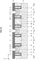
- FIG. 16 is a cross sectional view illustrating the semiconductor device according to the second embodiment.
- a plurality of emitter trenches 25 are formed in the first principal surface 10A, in addition to the plurality of gate trenches 21 and the plurality of emitter trenches 22.
- the emitter trenches 25 extend in the Y-direction, for example. Similar to the first embodiment, the pair of trenches 21, and the pair of trenches 22, are alternately arranged in the X-direction. In addition, two trenches 25 are arranged between the pair of trenches 21 and the pair of trenches 22 that are adjacent to each other.
- the distance between two trenches 21 that are adjacent to each other in the X-direction, the distance between two trenches 22 that are adjacent to each other in the X-direction, a distance between two trenches 25 that are adjacent to each other in the X-direction, a distance between the trenches 21 and 25 that are adjacent to each other in the X-direction, and a distance between the trenches 22 and 25 that are adjacent to each other in the X-direction, are the same. That is, if the trenches 21, 22, and 25 are not distinguished from one another, the plurality of trenches are equally spaced in the X-direction and formed in a stripe shape in the first principal surface 10A.
- the first region R1 is defined between two trenches 21 that are adjacent to each other in the X-direction
- the third region R3 is defined between two trenches 22 that are adjacent to each other in the X-direction.
- the second region R2 is defined between the trenches 21 and 25 that are adjacent to each other in the X-direction, between two trenches 25 that are adjacent to each other in the X-direction, and between the trenches 25 and 22 that are adjacent to each other in the X-direction.
- the first region R1 and the third region R3 are alternately disposed in the X-direction, with three second regions R2 interposed between the first region R1 and the third region R3, such that the third region R3, the three second regions R2, the first region R1, the three second regions R2, the third region R3, the three second regions R2, the first region R1, ..., are arranged in the X-direction.
- the P-type semiconductor layer 11 is provided in the first principal surface 10A.
- the P-type semiconductor layer 11 makes contact with two trenches (trenches 21 and 25, or trenches 25, or trenches 22 and 25) that define the second region R2 in the X-direction.
- the insulating film 30 is also provided on the inner wall of trench 25.
- An emitter trench electrode 45 is provided inside the trench 25 via the insulating film 30.
- the emitter trench electrode 45 may be formed using polysilicon, for example. Similar to the emitter trench electrode 42, the emitter trench electrode 45 is drawn out and routed to a vicinity of an outer periphery of the semiconductor device 200, for example, and is connected to the emitter electrode (or emitter pad) 61.
- the second embodiment can also obtain the advantageous features or effects obtainable by the first embodiment.
- the effects of the IE can further be improved, and the saturation voltage Vce(sat) can further be reduced to improve the efficiency of the semiconductor device 200.
- the number of trenches 25 arranged between the pair of trenches 21 and the pair of trenches 22 that are adjacent to each other is not particularly limited, and the number of trenches 25 may be one or more, and three or more.
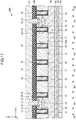
- FIG. 17 is a cross sectional view illustrating the semiconductor device according to the third embodiment.
- a plurality of gate trenches 26 are formed in the first principal surface 10A in addition to the plurality of gate trenches 21, the plurality of emitter trenches 22, and the plurality of emitter trenches 25.
- the trenches 26 extend in the Y-direction, for example. Similar to the second embodiment, the pair of trenches 21 and the pair of trenches 22 are alternately arranged in the X-direction.
- two trenches 25 are arranged between the pair of trenches 21 and the pair of trenches 22 that are adjacent to each other. Further, one trench 26 is arranged between the two trenches 25 that are adjacent to each other.
- the distance between two trenches 21 adjacent to each other in the X-direction, the distance between two trenches 22 adjacent to each other in the X-direction, the distance between the trenches 21 and 25 adjacent to each other in the X-direction, a distance between the trenches 25 and 26 adjacent to each other in the X-direction, and the distance between the trenches 22 and 25 adjacent to each other in the X-direction, are the same. That is, if the trenches 21, 22, 25, and 26 are not distinguished from one another, the plurality of trenches are equally spaced in the X-direction and formed in a stripe shape in the first principal surface 10A.
- the first region R1 is defined between two trenches 21 adjacent to each other in the X-direction
- the third region R3 is defined between two trenches 22 adjacent to each other in the X-direction
- the second region R2 is defined between the trenches 21 and 25 adjacent to each other in the X-direction, between two trenches 25 adjacent to each other in the X-direction, between the trenches 25 and 26 adjacent to each other in the X-direction, and between the trenches 26 and 22 adjacent to each other in the X-direction.
- the first region R1 and the third region R3 are alternately disposed in the X-direction, with four second regions R2 interposed between the first region R1 and the third region R3, such that the third region R3, the four second regions R2, the first region R1, the four second regions R2, the third region R3, the four second regions R2, the first region R1, ..., are arranged in the X-direction.
- the P-type semiconductor layer 11 is provided in the first principal surface 10A.
- the P-type semiconductor layer 11 makes contact with two trenches (trenches 21 and 25, or trenches 25 and 26, or trenches 22 and 25) that define the second region R2 in the X-direction.
- the insulating film 30 is also provided on the inner wall of trench 26.
- a gate trench electrode 46 is provided inside the trench 26 via the insulating film 30.
- the gate trench electrode 46 may be formed using polysilicon, for example. Similar to the gate trench electrode 41, the gate trench electrode 46 is drawn out and routed to a vicinity of an outer periphery of the semiconductor device 300, for example, and is connected to the gate electrode (or gate pad), which is not illustrated.
- the third embodiment can also obtain the advantageous features or effects obtainable by the second embodiment.
- the input capacitance can be increased while avoiding the increase of the gate capacitance in the MOS structure affecting the properties of the IGBT. Hence, the gate noise can be reduced.
Landscapes
- Electrodes Of Semiconductors (AREA)
- Metal-Oxide And Bipolar Metal-Oxide Semiconductor Integrated Circuits (AREA)
Applications Claiming Priority (1)
| Application Number | Priority Date | Filing Date | Title |
|---|---|---|---|
| JP2020105121A JP7564425B2 (ja) | 2020-06-18 | 2020-06-18 | 半導体装置及びその製造方法 |
Publications (2)
| Publication Number | Publication Date |
|---|---|
| EP3926687A1 true EP3926687A1 (de) | 2021-12-22 |
| EP3926687B1 EP3926687B1 (de) | 2025-04-23 |
Family
ID=76444349
Family Applications (1)
| Application Number | Title | Priority Date | Filing Date |
|---|---|---|---|
| EP21179296.5A Active EP3926687B1 (de) | 2020-06-18 | 2021-06-14 | Halbleiterbauelement und verfahren zur herstellung des halbleiterbauelements |
Country Status (4)
| Country | Link |
|---|---|
| US (2) | US11569373B2 (de) |
| EP (1) | EP3926687B1 (de) |
| JP (2) | JP7564425B2 (de) |
| CN (1) | CN113823672A (de) |
Families Citing this family (1)
| Publication number | Priority date | Publication date | Assignee | Title |
|---|---|---|---|---|
| JP7564425B2 (ja) * | 2020-06-18 | 2024-10-09 | ミツミ電機株式会社 | 半導体装置及びその製造方法 |
Citations (7)
| Publication number | Priority date | Publication date | Assignee | Title |
|---|---|---|---|---|
| JPH08316479A (ja) | 1995-03-14 | 1996-11-29 | Mitsubishi Electric Corp | 絶縁ゲート型半導体装置およびその製造方法 |
| JP2008205015A (ja) | 2007-02-16 | 2008-09-04 | Mitsubishi Electric Corp | 半導体装置およびその製造方法 |
| US20120181575A1 (en) * | 2011-01-17 | 2012-07-19 | Infineon Technologies Austria Ag | Semiconductor Device and a Reverse Conducting IGBT |
| EP2546882A1 (de) * | 2010-03-09 | 2013-01-16 | Fuji Electric Co., Ltd. | Halbleiterbauelement |
| JP2014063961A (ja) * | 2012-09-24 | 2014-04-10 | Denso Corp | 半導体装置 |
| WO2015022989A1 (ja) * | 2013-08-15 | 2015-02-19 | 富士電機株式会社 | 半導体装置 |
| US20170054010A1 (en) * | 2015-08-21 | 2017-02-23 | Renesas Electronics Corporation | Semiconductor device and method of manufacturing same |
Family Cites Families (12)
| Publication number | Priority date | Publication date | Assignee | Title |
|---|---|---|---|---|
| JPS5222155Y2 (de) | 1973-12-15 | 1977-05-20 | ||
| US5751024A (en) | 1995-03-14 | 1998-05-12 | Mitsubishi Denki Kabushiki Kaisha | Insulated gate semiconductor device |
| US5894149A (en) * | 1996-04-11 | 1999-04-13 | Mitsubishi Denki Kabushiki Kaisha | Semiconductor device having high breakdown voltage and method of manufacturing the same |
| JP5594276B2 (ja) * | 2010-12-08 | 2014-09-24 | 株式会社デンソー | 絶縁ゲート型半導体装置 |
| JP6564821B2 (ja) * | 2012-08-21 | 2019-08-21 | ローム株式会社 | 半導体装置 |
| JP2014075483A (ja) * | 2012-10-04 | 2014-04-24 | Sanken Electric Co Ltd | 半導体装置及び半導体装置の製造方法 |
| JP6392133B2 (ja) * | 2015-01-28 | 2018-09-19 | 株式会社東芝 | 半導体装置 |
| CN107210322B (zh) * | 2015-07-07 | 2020-11-06 | 富士电机株式会社 | 半导体装置 |
| JP6624973B2 (ja) * | 2016-03-03 | 2019-12-25 | ルネサスエレクトロニクス株式会社 | 半導体装置 |
| CN109564943B (zh) * | 2017-02-13 | 2022-06-24 | 富士电机株式会社 | 半导体装置 |
| JP6584592B2 (ja) * | 2018-06-15 | 2019-10-02 | ルネサスエレクトロニクス株式会社 | トレンチゲートigbt |
| JP7564425B2 (ja) * | 2020-06-18 | 2024-10-09 | ミツミ電機株式会社 | 半導体装置及びその製造方法 |
-
2020
- 2020-06-18 JP JP2020105121A patent/JP7564425B2/ja active Active
-
2021
- 2021-04-28 CN CN202110470376.9A patent/CN113823672A/zh active Pending
- 2021-06-03 US US17/337,662 patent/US11569373B2/en active Active
- 2021-06-14 EP EP21179296.5A patent/EP3926687B1/de active Active
-
2022
- 2022-12-27 US US18/146,669 patent/US11769823B2/en active Active
-
2024
- 2024-09-24 JP JP2024165256A patent/JP7849620B2/ja active Active
Patent Citations (9)
| Publication number | Priority date | Publication date | Assignee | Title |
|---|---|---|---|---|
| JPH08316479A (ja) | 1995-03-14 | 1996-11-29 | Mitsubishi Electric Corp | 絶縁ゲート型半導体装置およびその製造方法 |
| JP3288218B2 (ja) | 1995-03-14 | 2002-06-04 | 三菱電機株式会社 | 絶縁ゲート型半導体装置およびその製造方法 |
| JP2008205015A (ja) | 2007-02-16 | 2008-09-04 | Mitsubishi Electric Corp | 半導体装置およびその製造方法 |
| JP5089191B2 (ja) | 2007-02-16 | 2012-12-05 | 三菱電機株式会社 | 半導体装置およびその製造方法 |
| EP2546882A1 (de) * | 2010-03-09 | 2013-01-16 | Fuji Electric Co., Ltd. | Halbleiterbauelement |
| US20120181575A1 (en) * | 2011-01-17 | 2012-07-19 | Infineon Technologies Austria Ag | Semiconductor Device and a Reverse Conducting IGBT |
| JP2014063961A (ja) * | 2012-09-24 | 2014-04-10 | Denso Corp | 半導体装置 |
| WO2015022989A1 (ja) * | 2013-08-15 | 2015-02-19 | 富士電機株式会社 | 半導体装置 |
| US20170054010A1 (en) * | 2015-08-21 | 2017-02-23 | Renesas Electronics Corporation | Semiconductor device and method of manufacturing same |
Also Published As
| Publication number | Publication date |
|---|---|
| US20210399118A1 (en) | 2021-12-23 |
| CN113823672A (zh) | 2021-12-21 |
| US20230135596A1 (en) | 2023-05-04 |
| US11769823B2 (en) | 2023-09-26 |
| EP3926687B1 (de) | 2025-04-23 |
| JP2024178358A (ja) | 2024-12-24 |
| US11569373B2 (en) | 2023-01-31 |
| JP2021197525A (ja) | 2021-12-27 |
| JP7849620B2 (ja) | 2026-04-22 |
| JP7564425B2 (ja) | 2024-10-09 |
Similar Documents
| Publication | Publication Date | Title |
|---|---|---|
| JP7327672B2 (ja) | 半導体装置 | |
| US5723890A (en) | MOS type semiconductor device | |
| JP4171268B2 (ja) | 半導体装置およびその製造方法 | |
| CN109659351B (zh) | 绝缘栅双极晶体管 | |
| US20210242342A1 (en) | Semiconductor device and method for manufacturing same | |
| CN102208367B (zh) | 半导体装置的制造方法 | |
| US6160288A (en) | Vertical type misfet having improved pressure resistance | |
| JP2020031167A (ja) | 半導体装置およびその製造方法 | |
| CN113921597A (zh) | 半导体装置以及半导体装置的制造方法 | |
| JPH04251983A (ja) | 半導体装置 | |
| JP2026063449A (ja) | 半導体装置およびその製造方法 | |
| JP4025063B2 (ja) | 半導体装置 | |
| US11769823B2 (en) | Semiconductor device and method for manufacturing semiconductor device | |
| US10418479B2 (en) | Semiconductor device and method of manufacturing semiconductor device | |
| JP7803419B2 (ja) | 炭化珪素半導体装置 | |
| US20240014267A1 (en) | Semiconductor device | |
| US20240113189A1 (en) | Semiconductor device and method of manufacturing the same | |
| JP2021150405A (ja) | 炭化珪素半導体装置 | |
| JP7821079B2 (ja) | 半導体装置およびその製造方法 | |
| CN115917755B (zh) | 碳化硅半导体装置 | |
| WO2023127253A1 (ja) | 半導体装置 | |
| JP4400035B2 (ja) | 絶縁ゲート型半導体素子及び絶縁ゲート型半導体素子の製造方法 | |
| JP3381490B2 (ja) | Mos型半導体装置 | |
| JP2023113080A (ja) | 半導体装置および半導体装置の製造方法 | |
| US20250241040A1 (en) | Gate trench power semiconductor devices having deep trench shield connection patterns |
Legal Events
| Date | Code | Title | Description |
|---|---|---|---|
| PUAI | Public reference made under article 153(3) epc to a published international application that has entered the european phase |
Free format text: ORIGINAL CODE: 0009012 |
|
| STAA | Information on the status of an ep patent application or granted ep patent |
Free format text: STATUS: THE APPLICATION HAS BEEN PUBLISHED |
|
| AK | Designated contracting states |
Kind code of ref document: A1 Designated state(s): AL AT BE BG CH CY CZ DE DK EE ES FI FR GB GR HR HU IE IS IT LI LT LU LV MC MK MT NL NO PL PT RO RS SE SI SK SM TR |
|
| B565 | Issuance of search results under rule 164(2) epc |
Effective date: 20211025 |
|
| STAA | Information on the status of an ep patent application or granted ep patent |
Free format text: STATUS: REQUEST FOR EXAMINATION WAS MADE |
|
| 17P | Request for examination filed |
Effective date: 20220221 |
|
| RBV | Designated contracting states (corrected) |
Designated state(s): AL AT BE BG CH CY CZ DE DK EE ES FI FR GB GR HR HU IE IS IT LI LT LU LV MC MK MT NL NO PL PT RO RS SE SI SK SM TR |
|
| STAA | Information on the status of an ep patent application or granted ep patent |
Free format text: STATUS: EXAMINATION IS IN PROGRESS |
|
| 17Q | First examination report despatched |
Effective date: 20240912 |
|
| GRAP | Despatch of communication of intention to grant a patent |
Free format text: ORIGINAL CODE: EPIDOSNIGR1 |
|
| STAA | Information on the status of an ep patent application or granted ep patent |
Free format text: STATUS: GRANT OF PATENT IS INTENDED |
|
| INTG | Intention to grant announced |
Effective date: 20241204 |
|
| GRAS | Grant fee paid |
Free format text: ORIGINAL CODE: EPIDOSNIGR3 |
|
| GRAA | (expected) grant |
Free format text: ORIGINAL CODE: 0009210 |
|
| STAA | Information on the status of an ep patent application or granted ep patent |
Free format text: STATUS: THE PATENT HAS BEEN GRANTED |
|
| AK | Designated contracting states |
Kind code of ref document: B1 Designated state(s): AL AT BE BG CH CY CZ DE DK EE ES FI FR GB GR HR HU IE IS IT LI LT LU LV MC MK MT NL NO PL PT RO RS SE SI SK SM TR |
|
| REG | Reference to a national code |
Ref country code: GB Ref legal event code: FG4D |
|
| REG | Reference to a national code |
Ref country code: DE Ref legal event code: R096 Ref document number: 602021029479 Country of ref document: DE |
|
| REG | Reference to a national code |
Ref country code: IE Ref legal event code: FG4D |
|
| P01 | Opt-out of the competence of the unified patent court (upc) registered |
Free format text: CASE NUMBER: APP_21984/2025 Effective date: 20250508 |
|
| PGFP | Annual fee paid to national office [announced via postgrant information from national office to epo] |
Ref country code: DE Payment date: 20250618 Year of fee payment: 5 |
|
| PGFP | Annual fee paid to national office [announced via postgrant information from national office to epo] |
Ref country code: AT Payment date: 20250721 Year of fee payment: 5 |
|
| REG | Reference to a national code |
Ref country code: NL Ref legal event code: MP Effective date: 20250423 |
|
| PG25 | Lapsed in a contracting state [announced via postgrant information from national office to epo] |
Ref country code: NL Free format text: LAPSE BECAUSE OF FAILURE TO SUBMIT A TRANSLATION OF THE DESCRIPTION OR TO PAY THE FEE WITHIN THE PRESCRIBED TIME-LIMIT Effective date: 20250423 |
|
| REG | Reference to a national code |
Ref country code: AT Ref legal event code: MK05 Ref document number: 1788678 Country of ref document: AT Kind code of ref document: T Effective date: 20250423 |
|
| PG25 | Lapsed in a contracting state [announced via postgrant information from national office to epo] |
Ref country code: FI Free format text: LAPSE BECAUSE OF FAILURE TO SUBMIT A TRANSLATION OF THE DESCRIPTION OR TO PAY THE FEE WITHIN THE PRESCRIBED TIME-LIMIT Effective date: 20250423 Ref country code: PT Free format text: LAPSE BECAUSE OF FAILURE TO SUBMIT A TRANSLATION OF THE DESCRIPTION OR TO PAY THE FEE WITHIN THE PRESCRIBED TIME-LIMIT Effective date: 20250825 Ref country code: ES Free format text: LAPSE BECAUSE OF FAILURE TO SUBMIT A TRANSLATION OF THE DESCRIPTION OR TO PAY THE FEE WITHIN THE PRESCRIBED TIME-LIMIT Effective date: 20250423 |
|
| REG | Reference to a national code |
Ref country code: LT Ref legal event code: MG9D |
|
| PG25 | Lapsed in a contracting state [announced via postgrant information from national office to epo] |
Ref country code: GR Free format text: LAPSE BECAUSE OF FAILURE TO SUBMIT A TRANSLATION OF THE DESCRIPTION OR TO PAY THE FEE WITHIN THE PRESCRIBED TIME-LIMIT Effective date: 20250724 Ref country code: NO Free format text: LAPSE BECAUSE OF FAILURE TO SUBMIT A TRANSLATION OF THE DESCRIPTION OR TO PAY THE FEE WITHIN THE PRESCRIBED TIME-LIMIT Effective date: 20250723 |
|
| PG25 | Lapsed in a contracting state [announced via postgrant information from national office to epo] |
Ref country code: PL Free format text: LAPSE BECAUSE OF FAILURE TO SUBMIT A TRANSLATION OF THE DESCRIPTION OR TO PAY THE FEE WITHIN THE PRESCRIBED TIME-LIMIT Effective date: 20250423 |
|
| PG25 | Lapsed in a contracting state [announced via postgrant information from national office to epo] |
Ref country code: BG Free format text: LAPSE BECAUSE OF FAILURE TO SUBMIT A TRANSLATION OF THE DESCRIPTION OR TO PAY THE FEE WITHIN THE PRESCRIBED TIME-LIMIT Effective date: 20250423 |
|
| PG25 | Lapsed in a contracting state [announced via postgrant information from national office to epo] |
Ref country code: HR Free format text: LAPSE BECAUSE OF FAILURE TO SUBMIT A TRANSLATION OF THE DESCRIPTION OR TO PAY THE FEE WITHIN THE PRESCRIBED TIME-LIMIT Effective date: 20250423 |
|
| PG25 | Lapsed in a contracting state [announced via postgrant information from national office to epo] |
Ref country code: AT Free format text: LAPSE BECAUSE OF FAILURE TO SUBMIT A TRANSLATION OF THE DESCRIPTION OR TO PAY THE FEE WITHIN THE PRESCRIBED TIME-LIMIT Effective date: 20250423 |
|
| PG25 | Lapsed in a contracting state [announced via postgrant information from national office to epo] |
Ref country code: RS Free format text: LAPSE BECAUSE OF FAILURE TO SUBMIT A TRANSLATION OF THE DESCRIPTION OR TO PAY THE FEE WITHIN THE PRESCRIBED TIME-LIMIT Effective date: 20250723 |
|
| PG25 | Lapsed in a contracting state [announced via postgrant information from national office to epo] |
Ref country code: IS Free format text: LAPSE BECAUSE OF FAILURE TO SUBMIT A TRANSLATION OF THE DESCRIPTION OR TO PAY THE FEE WITHIN THE PRESCRIBED TIME-LIMIT Effective date: 20250823 |
|
| PG25 | Lapsed in a contracting state [announced via postgrant information from national office to epo] |
Ref country code: LV Free format text: LAPSE BECAUSE OF FAILURE TO SUBMIT A TRANSLATION OF THE DESCRIPTION OR TO PAY THE FEE WITHIN THE PRESCRIBED TIME-LIMIT Effective date: 20250423 |
|
| PG25 | Lapsed in a contracting state [announced via postgrant information from national office to epo] |
Ref country code: SM Free format text: LAPSE BECAUSE OF FAILURE TO SUBMIT A TRANSLATION OF THE DESCRIPTION OR TO PAY THE FEE WITHIN THE PRESCRIBED TIME-LIMIT Effective date: 20250423 Ref country code: DK Free format text: LAPSE BECAUSE OF FAILURE TO SUBMIT A TRANSLATION OF THE DESCRIPTION OR TO PAY THE FEE WITHIN THE PRESCRIBED TIME-LIMIT Effective date: 20250423 |
|
| PG25 | Lapsed in a contracting state [announced via postgrant information from national office to epo] |
Ref country code: CZ Free format text: LAPSE BECAUSE OF FAILURE TO SUBMIT A TRANSLATION OF THE DESCRIPTION OR TO PAY THE FEE WITHIN THE PRESCRIBED TIME-LIMIT Effective date: 20250423 |
|
| PG25 | Lapsed in a contracting state [announced via postgrant information from national office to epo] |
Ref country code: EE Free format text: LAPSE BECAUSE OF FAILURE TO SUBMIT A TRANSLATION OF THE DESCRIPTION OR TO PAY THE FEE WITHIN THE PRESCRIBED TIME-LIMIT Effective date: 20250423 |
|
| REG | Reference to a national code |
Ref country code: DE Ref legal event code: R097 Ref document number: 602021029479 Country of ref document: DE |
|
| PG25 | Lapsed in a contracting state [announced via postgrant information from national office to epo] |
Ref country code: RO Free format text: LAPSE BECAUSE OF FAILURE TO SUBMIT A TRANSLATION OF THE DESCRIPTION OR TO PAY THE FEE WITHIN THE PRESCRIBED TIME-LIMIT Effective date: 20250423 Ref country code: SK Free format text: LAPSE BECAUSE OF FAILURE TO SUBMIT A TRANSLATION OF THE DESCRIPTION OR TO PAY THE FEE WITHIN THE PRESCRIBED TIME-LIMIT Effective date: 20250423 |
|
| REG | Reference to a national code |
Ref country code: CH Ref legal event code: H13 Free format text: ST27 STATUS EVENT CODE: U-0-0-H10-H13 (AS PROVIDED BY THE NATIONAL OFFICE) Effective date: 20260127 |
|
| PG25 | Lapsed in a contracting state [announced via postgrant information from national office to epo] |
Ref country code: IT Free format text: LAPSE BECAUSE OF FAILURE TO SUBMIT A TRANSLATION OF THE DESCRIPTION OR TO PAY THE FEE WITHIN THE PRESCRIBED TIME-LIMIT Effective date: 20250423 |
|
| PG25 | Lapsed in a contracting state [announced via postgrant information from national office to epo] |
Ref country code: MC Free format text: LAPSE BECAUSE OF FAILURE TO SUBMIT A TRANSLATION OF THE DESCRIPTION OR TO PAY THE FEE WITHIN THE PRESCRIBED TIME-LIMIT Effective date: 20250423 |
|
| PG25 | Lapsed in a contracting state [announced via postgrant information from national office to epo] |
Ref country code: LU Free format text: LAPSE BECAUSE OF NON-PAYMENT OF DUE FEES Effective date: 20250614 |
|
| REG | Reference to a national code |
Ref country code: BE Ref legal event code: MM Effective date: 20250630 |
|
| PLBE | No opposition filed within time limit |
Free format text: ORIGINAL CODE: 0009261 |
|
| STAA | Information on the status of an ep patent application or granted ep patent |
Free format text: STATUS: NO OPPOSITION FILED WITHIN TIME LIMIT |
|
| REG | Reference to a national code |
Ref country code: CH Ref legal event code: L10 Free format text: ST27 STATUS EVENT CODE: U-0-0-L10-L00 (AS PROVIDED BY THE NATIONAL OFFICE) Effective date: 20260304 |
|
| GBPC | Gb: european patent ceased through non-payment of renewal fee |
Effective date: 20250723 |
|
| 26N | No opposition filed |
Effective date: 20260126 |
|
| PG25 | Lapsed in a contracting state [announced via postgrant information from national office to epo] |
Ref country code: GB Free format text: LAPSE BECAUSE OF NON-PAYMENT OF DUE FEES Effective date: 20250723 |
|
| PG25 | Lapsed in a contracting state [announced via postgrant information from national office to epo] |
Ref country code: IE Free format text: LAPSE BECAUSE OF NON-PAYMENT OF DUE FEES Effective date: 20250614 |
|
| PG25 | Lapsed in a contracting state [announced via postgrant information from national office to epo] |
Ref country code: BE Free format text: LAPSE BECAUSE OF NON-PAYMENT OF DUE FEES Effective date: 20250630 |
|
| PG25 | Lapsed in a contracting state [announced via postgrant information from national office to epo] |
Ref country code: FR Free format text: LAPSE BECAUSE OF NON-PAYMENT OF DUE FEES Effective date: 20250623 |
|
| PG25 | Lapsed in a contracting state [announced via postgrant information from national office to epo] |
Ref country code: CH Free format text: LAPSE BECAUSE OF NON-PAYMENT OF DUE FEES Effective date: 20250630 |